EP0736968A2 - Circuit amplificateur pour supprimer la tension de décalage - Google Patents
Circuit amplificateur pour supprimer la tension de décalage Download PDFInfo
- Publication number
- EP0736968A2 EP0736968A2 EP96302480A EP96302480A EP0736968A2 EP 0736968 A2 EP0736968 A2 EP 0736968A2 EP 96302480 A EP96302480 A EP 96302480A EP 96302480 A EP96302480 A EP 96302480A EP 0736968 A2 EP0736968 A2 EP 0736968A2
- Authority
- EP
- European Patent Office
- Prior art keywords
- offset
- amplifier
- signal
- circuit
- input
- Prior art date
- Legal status (The legal status is an assumption and is not a legal conclusion. Google has not performed a legal analysis and makes no representation as to the accuracy of the status listed.)
- Withdrawn
Links
- 230000003287 optical effect Effects 0.000 claims abstract description 35
- 238000001514 detection method Methods 0.000 claims abstract description 31
- 239000003990 capacitor Substances 0.000 description 7
- 230000003321 amplification Effects 0.000 description 6
- 238000003199 nucleic acid amplification method Methods 0.000 description 6
- 230000001419 dependent effect Effects 0.000 description 4
- 229920006395 saturated elastomer Polymers 0.000 description 2
- 230000002411 adverse Effects 0.000 description 1
Images




Classifications
-
- H—ELECTRICITY
- H03—ELECTRONIC CIRCUITRY
- H03F—AMPLIFIERS
- H03F3/00—Amplifiers with only discharge tubes or only semiconductor devices as amplifying elements
- H03F3/45—Differential amplifiers
- H03F3/45071—Differential amplifiers with semiconductor devices only
- H03F3/45479—Differential amplifiers with semiconductor devices only characterised by the way of common mode signal rejection
- H03F3/45928—Differential amplifiers with semiconductor devices only characterised by the way of common mode signal rejection using IC blocks as the active amplifying circuit
- H03F3/45932—Differential amplifiers with semiconductor devices only characterised by the way of common mode signal rejection using IC blocks as the active amplifying circuit by using feedback means
- H03F3/45937—Measuring at the loading circuit of the differential amplifier
- H03F3/45941—Controlling the input circuit of the differential amplifier
-
- H—ELECTRICITY
- H03—ELECTRONIC CIRCUITRY
- H03F—AMPLIFIERS
- H03F3/00—Amplifiers with only discharge tubes or only semiconductor devices as amplifying elements
- H03F3/04—Amplifiers with only discharge tubes or only semiconductor devices as amplifying elements with semiconductor devices only
- H03F3/08—Amplifiers with only discharge tubes or only semiconductor devices as amplifying elements with semiconductor devices only controlled by light
- H03F3/087—Amplifiers with only discharge tubes or only semiconductor devices as amplifying elements with semiconductor devices only controlled by light with IC amplifier blocks
-
- H—ELECTRICITY
- H03—ELECTRONIC CIRCUITRY
- H03F—AMPLIFIERS
- H03F3/00—Amplifiers with only discharge tubes or only semiconductor devices as amplifying elements
- H03F3/45—Differential amplifiers
- H03F3/45071—Differential amplifiers with semiconductor devices only
- H03F3/45479—Differential amplifiers with semiconductor devices only characterised by the way of common mode signal rejection
- H03F3/45928—Differential amplifiers with semiconductor devices only characterised by the way of common mode signal rejection using IC blocks as the active amplifying circuit
- H03F3/45968—Differential amplifiers with semiconductor devices only characterised by the way of common mode signal rejection using IC blocks as the active amplifying circuit by offset reduction
- H03F3/45973—Differential amplifiers with semiconductor devices only characterised by the way of common mode signal rejection using IC blocks as the active amplifying circuit by offset reduction by using a feedback circuit
-
- H—ELECTRICITY
- H03—ELECTRONIC CIRCUITRY
- H03F—AMPLIFIERS
- H03F2203/00—Indexing scheme relating to amplifiers with only discharge tubes or only semiconductor devices as amplifying elements covered by H03F3/00
- H03F2203/45—Indexing scheme relating to differential amplifiers
- H03F2203/45511—Indexing scheme relating to differential amplifiers the feedback circuit [FBC] comprising one or more transistor stages, e.g. cascaded stages of the dif amp, and being coupled between the loading circuit [LC] and the input circuit [IC]
-
- H—ELECTRICITY
- H03—ELECTRONIC CIRCUITRY
- H03F—AMPLIFIERS
- H03F2203/00—Indexing scheme relating to amplifiers with only discharge tubes or only semiconductor devices as amplifying elements covered by H03F3/00
- H03F2203/45—Indexing scheme relating to differential amplifiers
- H03F2203/45526—Indexing scheme relating to differential amplifiers the FBC comprising a resistor-capacitor combination and being coupled between the LC and the IC
Definitions
- This invention relates to an optical receiver circuit for use in optical communication, optical interconnection, and the like and, in particular, to an offset cancelling amplifier used in the optical receiver circuit.
- a conventional optical receiver circuit comprises a photodetector section responsive to an optical signal for converting the optical signal into a unipolar input current pulse signal and a polarity converter section for converting the unipolar input current pulse signal into a bipolar voltage pulse signal.
- the polarity converter section comprises a pre-amplifier or transimpedance amplifier and an offset cancelling amplifier circuit cascaded to the pre-amplifier and is integrated on a single chip.
- offset involves both an internal offset occurring within the offset cancelling amplifier circuit and an external offset of an outside origin.
- optical receiver circuit with the offset cancelling amplifier circuit of the type described is disclosed, for example, in Japanese Patent Pre-examination Publication (A) No. 15909/1987 (Reference I).
- the offset cancelling amplifier circuit shown in the Reference I comprises a limiting amplifier having an input circuit for amplifying an input signal incoming through the input circuit while preventing amplified amplitude from exceeding a predetermined level to provide an output signal, an offset detector for detecting an offset in the output signal to produce a detection signal representing an offset amount detected, and an offset controller coupled in the input circuit of the limiting amplifier and the offset detector for controlling an input voltage of the limiting amplifier in response to the detection signal to reduce or cancel the offset in the output signal.
- the offset detector forms a feedback loop for feeding back the offset in the output signal to the input circuit.
- the offset detector comprises a CR integrator circuit including a capacitor and a resistor, and a feedback differential amplifier for acquiring a necessary and sufficient gain in a feedback loop.
- the offset in its output signal must be reduced as much as possible. This is achieved by increasing the gain (G) of the feedback differential amplifier. While, a low-frequency cutoff or a lower side cutoff frequency of the offset detector is determined by G/2 ⁇ CR, that is a product of the gain (G) of the feedback differential amplifier and a low-frequency cutoff (1/2 ⁇ CR) of the CR integrator circuit. Thus, the low-frequency cutoff of the offset detector can not be lowered. As a result, the offset cancelling amplifier circuit cannot be obtained with the low-frequency cutoff of a lowered frequency as well as the wide dynamic range.
- an offset cancelling amplifier circuit which comprises a limiting amplifier having an input circuit for amplifying an input signal incoming through the input circuit while preventing amplified amplitude from exceeding a predetermined level to provide an output signal, an offset detector comprising a Miller integrator for detecting an offset in the output signal to produce a detection signal representing an offset amount detected, and an offset controller coupled in the input circuit of the limiting amplifier and the offset detector for controlling an input voltage of the limiting amplifier in response to the detection signal to reduce the offset in the output signal for offset cancellation.
- the offset cancelling amplifier circuit of this invention has a low-frequency cutoff 1/2 ⁇ CR which is determined by a capacitance C and a resistance R of the Miller integrator but is not dependent upon a gain of the Miller integrator. Accordingly, the offset cancelling amplifier circuit has the capacitor and the resistor of relatively low capacitance C and resistance R, respectively, and is therefore adapted for an integrated circuit with a widened dynamic range and a lowered low-frequency cutoff.
- the known offset cancelling amplifier circuit comprises a limiting amplifier 11, an offset detector 12, and an offset controller 13.
- the limiting amplifier 11 amplifies the input voltage signal into an amplified voltage signal while preventing the amplified amplitude from exceeding a predetermined level to produce an output voltage signal at a pair of output terminals C and D.
- the input voltage signal comprises a pair of unipolar voltage signals, a first one of which is resulted from a photo-detection signal detected at a photodetector and applied to one input terminal A, the other second one being applied to the other terminal B and being an opposite polarity voltage signal having a polarity opposite to a polarity of the first unipolar voltage signal.
- an optical signal received in the optical receiver is a pulse signal having an average duty ratio or an average mark-to-space ratio of 50%, and therefore, the first unipolar voltage signal also has an average duty ratio of 50%.
- the second unipolar voltage signal is a reference signal which may be a constant voltage signal of the opposite polarity or a unipolar voltage pulse signal similar to the first unipolar voltage signal but with the opposite polarity.
- the output signal comprises a pair of bipolar signals, a first one of which is delivered at one output terminal C, while the other second one being delivered at the other output terminal D and having a reversed polarity in connection with the first bipolar voltage signal.
- the offset detector 12 is responsive to the output voltage signal and detects an offset in the output voltage signal to produce an offset detection signal representative of the offset amount detected.
- the offset detector 12 comprises a first CR integrator 12a, a second CR integrator 12b, and a feedback differential amplifier 12c.
- the offset detector 12 detects a first time average of the first bipolar voltage signal at terminal C and a second time average of the second bipolar voltage signal at terminal D and provides, as the offset detection signal, a detection voltage signal representative of the first and the second time averages.
- the first and the second time average signals are equal to each other when the output signal has no offset.
- the offset controller 13 is connected to an input circuit of the limiting amplifier 11 and is responsive to the offset detection signal for controlling a voltage at an input side of the limiting amplifier 11 to reduce or cancel the offset in the output signal of the limiting amplifier 11.
- the offset controller 13 comprises a current source 13a, a pair of transistors 13b and 13c, and two pairs of resistors 13d-13g.
- the offset in the output signal of the limiting amplifier 11 is detected by the offset detector 12 and is fed back to the input side of the limiting amplifier 11.
- This offset cancelling amplifier has a disadvantage that the low-frequency cutoff can not sufficiently be lowered if a gain (G) of the feedback differential amplifier 12c is increased so as to widen a dynamic range of the offset cancelling amplifier. This is because the low-frequency cutoff G/2 ⁇ CR is dependent upon the gain G of the feedback differential amplifier 12c of the offset detector 12, as described in the preamble of the specification.
- the offset cancelling amplifier circuit is similar to the known circuit of Fig. 1 and comprises the limiting amplifier 11 comprising a differential amplifier, the offset detector 12, and the offset controller 13.
- the offset cancelling amplifier circuit of this invention is different from the known circuit in that the offset detector 12 comprises a Miller integrator.
- the limiting amplifier 11 is an amplitude-limiting amplifier. Supplied with the input voltage signal, the limiting amplifier 11 amplifies the input voltage signal into an amplified voltage signal while preventing an amplified amplitude from exceeding a predetermined level.
- the limiting amplifier 11 is implemented by a known differential amplifier.
- the limiting amplifier 11 can be implemented by a single-stage differential amplifier. However, in order to obtain a sufficient gain for a low-energy signal, the limiting amplifier 11 preferably comprises a plurality of stages of the similar differential amplifiers connected in cascade. This is because the limiting amplifier comprising such multi-stage differential amplifiers connected in cascade achieves a high gain. In this structure, any circuit constant such as a source voltage is selected so that the first-stage differential amplifier is not saturated upon supply of a high-energy signal. In this event, the second and the subsequent differential amplifiers are prevented from being saturated. When the source voltage is selected as described above, the limiting amplifier 11 produces the output signal having an amplitude limited below the predetermined level in a wide dynamic range between a minimum input amplitude and a maximum input amplitude.
- the limiting amplifier 11 amplifies the input voltage signal incoming through input terminals A and B and produces the output signal at the output terminals C and D.
- the output signal comprises a pair of the first and the second bipolar voltage signals at terminals C and D, respectively.
- the offset detector 12 comprises the Miller integrator for comparing time averages of the first and second bipolar voltage signals at terminals C and D to obtain a differential time average and for amplifying the differential time average to produce an offset detection signal.
- the Miller integrator comprises an amplifier 121, first and second input resistors 122 and 123 having one ends connected to input terminals of the amplifier 121, first and second feedback capacitors 124 and 125 connected between the output and the input terminals of the amplifier 121 to form feedback loops corresponding to the first and the second input resistors 122 and 123, respectively.
- the first and the second input resistors 122 and 123 have a same resistance R.
- the first and the second feedback capacitors 124 and 125 have a same capacitance C.
- the offset detector (Miller integrator) 12 has an amplification gain G owing to the amplifier 121.
- the offset detector (Miller integrator) 12 has a time constant determined by the resistance R of the first and the second resistors 122 and 123 and the capacitance C of the first and the second feedback capacitors 124 and 125.
- the Miller integrator By the use of the Miller integrator as the offset detector 12, it is possible to obtain those values amplified by the amplification gain G and averaged by the time constant.
- the offset cancelling amplifier circuit since the offset detector 12 comprises the Miller integrator as described above, the low-frequency cutoff of the offset cancelling amplifier circuit is determined by the time constant of the Miller integrator to be equal to 1/2 ⁇ CR and is not dependent upon the gain G of the amplifier 121.
- the offset cancelling amplifier circuit of this invention is capable of both keeping the low-frequency cutoff at a lowered frequency and the dynamic range wide.
- the input unipolar voltage signals have an average duty ratio equal to 50%.
- the time averages of the first and the second bipolar voltage signals at terminals C and D are equal to each other. It is therefore possible to detect presence or absence of the offset with reference to the offset detection signal representative of the difference between the time averages.
- the offset controller 13 is supplied with the offset detection signal from the offset detector 12 and controls an input voltage potential of the input signal to be supplied to the limiting amplifier 11 so as to cancel the offset in the output signal.
- the offset controller 13 comprises a first subtractor 131 and a second subtractor 132.
- the first subtractor 131 subtracts the first time average signal from the first unipolar voltage signal applied to the input terminal A.
- the second subtractor 132 subtracts the second time average signal from the second unipolar voltage signal applied to the input terminal B.
- the input signal controlled by the offset controller 13 is applied to the limiting amplifier 11.
- the limiting amplifier 11 comprises the multi-stage differential amplifiers connected in cascade
- the differential amplifiers of the second and the subsequent stages are successively connected to the output terminals C and D in Fig. 2.
- input voltage potentials of differential amplifiers of the second and the subsequent stages need not be controlled, as described in the foregoing.
- a pair of unipolar voltage signals with opposite polarities or a pair of differential input signals having an external offset are supplied to the input terminals A and B, respectively, as illustrated in Fig. 3.
- a unipolar input signal can be supplied to the input terminal A but a constant voltage potential is maintained at the input terminal B, as illustrated in Fig. 4.
- the input signal supplied to the input terminals A and B are sent through the offset controller 13 to the limiting amplifier 11.
- the limiting amplifier 11 amplifies the input signal at a predetermined amplification factor into amplified signals with an amplitude limited so as not to exceed a predetermined level.
- the operation of the limiting amplifier 1 will hereafter be referred to as a limiting amplification operation.
- the output signal after the limiting amplification operation is delivered to the output terminals C and D.
- the output signal comprises a pair of bipolar voltage signals having reversed polarities to each other which are present at output terminals C and D, respectively.
- the offset detector 12 When the output signal has an offset, the offset detector 12 produces an offset detection signal representative of a detected offset amount and supplies the offset detection signal to the offset controller 13.
- the offset controller 13 controls the input voltage signal, in detail, input voltage potentials of the pair of unipolar voltage signals supplied to the input terminals A and B so as to cancel the offset present in the output signal.
- the limiting amplifier 11 Supplied with the input signal controlled by the offset controller 13, the limiting amplifier 11 performs the limiting amplification operation and produces the output signal at the output terminals C and D. Thus, the offset in the output signal is reduced or cancelled.
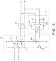
- the offset cancelling amplifier includes a specific example of the offset controller 13 comprises first and second controllable current sources 131 and 132, first and second transistors 133 and 134, and first and second resistors 135 and 136.
- the first and the second controllable current sources 131 and 132 are controlled by the offset detection signal, in detail, the first and the second time average signals of the offset detector 12, respectively.
- the first transistor 133 has a base connected to the input terminal A.
- the second transistor 134 has a base connected to the input terminal B.
- the first resistor 135 has one end connected to the first controllable current source 131 and the other end connected to an emitter of the first transistor 133.
- the second resistor 136 has one end connected to the second controllable current source 132 and the other end connected to an emitter of the second transistor 134.
- the offset controller 13 has power supply terminals l , m, n and p.
- a common connection point I1 between the first controllable current source 131 and the first resistor 135 and another common connection point I2 between the second controllable current source 132 and the second resistor 136 are connected to the limiting amplifier 11.
- the pair of first and second opposite polarity voltage signals at A and B are amplified and present at the connection points at I1 and I2, respectively.
- the first and the second controllable current sources 131 and 132 are controlled by the offset detection signal.
- the voltage potentials at connection points at I1 and I2 are controlled by the offset detection signal.
- the input signal is controlled by the the offset controller 13 in response to the offset detection signal and is applied to the limiting amplifier 11.
- the offset controller 13 applicable to the offset cancelling amplifier circuit of this invention is not restricted to the offset controller illustrated in Fig. 6 and may have various structures.
- the offset controller 13 shown in Fig. 1 is also applicable to the offset cancelling amplifier of this invention.
- the photo-detector section 14 comprises a photo-detector element such as a photo-diode.
- the pre-amplifier section 15 comprises first and second pre-amplifiers 151 and 152.
- the first pre-amplifier 151 comprises a first amplifier 1511 and a first feedback resistor 1512.
- the second pre-amplifier 152 comprises a second amplifier 1521 and a second feedback resistor 1522.
- the photo-detector section 14 is connected to a power source (not shown) through a terminal a.
- the photo-detector section 14 is connected through a terminal b to the first pre-amplifier 151.
- the second pre-amplifier 152 is connected through a terminal c to a reference signal source (not shown) for producing a predetermined reference signal.
- the first pre-amplifier 151 is connected via a terminal d to the input terminal A of the offset cancelling amplifier circuit described before.
- the second pre-amplifier 152 is connected via a terminal e to the input terminal B of the offset cancelling amplifier circuit.
- the photo-detector 14 converts the optical signal into an input current pulse signal to deliver the input current pulse signal to the terminal b.
- the first pre-amplifier 151 amplifies and converts the input current signal into a unipolar voltage signal which is applied to the input terminal A of the offset cancelling amplifier circuit of Fig. 2 through the terminal d.
- the second pre-amplifier 152 amplifies and converts into a reference voltage signal of a unipolar which is applied to the input terminal B of the offset cancelling amplifier circuit of Fig. 2 through the the terminal e.
- the input terminals A and B of the offset cancelling amplifier circuit are supplied with the unipolar voltage signals as illustrated in Fig. 3 or Fig. 4.
- the unipolar voltage signals are as shown in Fig. 3.
- the reference signal is a constant voltage signal
- the unipolar voltage signal is as shown in Fig. 4.
- FIG. 8 another example of the pre-amplifier section 15 is shown together with the photo-detector section 14 connected thereto.
- the pre-amplifier section 15 of this example comprises a differential amplifier 15a and first and second feedback resistors 15b and 15c.
- those terminals connected in the similar manner as described in conjunction with Fig. 7 are designated by like reference symbols.
- the pre-amplifier section 15 illustrated in Fig. 8 carries out an operation basically similar to that of the pre-amplifier section 15 illustrated in Fig. 7.
- the pre-amplifier section 15 in Fig. 8 comprises a single one of the differential amplifier 15a which amplifies the input current pulse signal from the photo-detector section 14 to produce a pair of differential signals.
- the differential signals are applied to, as the first and the second unipolar voltage signals as shown in Fig. 3, the input terminals A and B of the offset cancelling amplifier circuit.
- FIG. 9 another example of the pre-amplifier section 15 is shown together with the photo-detector section 14 connected thereto.
- a pre-amplifier section 15 comprises first and second pre-amplifiers 151 and 152.
- the first pre-amplifier 151 comprises a first transistor Tr1 having an emitter and a collector which are connected to opposite terminals f and h of a power source (not shown) through a first and a second resistors R1a and R1b.
- the transistor Tr1 has a base which is connected to a voltage source S1 illustrated as an electric cell.
- a connection point between the emitter of the transistor Tr1 and the first resistor R1a is connected to the photo-detector section 14 through an input terminal b.
- Another connection point between the collector of the transistor Tr1 and the second resistor R1b is connected to an output terminal d which is connected to an input terminal A of the offset cancelling amplifier of Fig. 2.
- the second pre-amplifier 152 has a similar structure and comprises a transistor Tr2 having an emitter and a collector which are connected to opposite terminals g and i of a power source (not shown) through first and second resistors R2a and R2b.
- the transistor Tr2 has a base which is connected to a voltage source 52 illustrated as an electric cell.
- a connection point between the emitter of the transistor Tr2 and the first resistor R2a is connected to the reference signal source (not shown) through an input terminal c.
- Another connection point between the collector of the transistor Tr2 and the second resistor R2b is connected to an output terminal e which is connected to an input terminal B of the offset cancelling amplifier of Fig. 2.
- the pre-amplifier section 15 of this example carries out an operation basically similar to that of the pre-amplifier section 15 illustrated in Fig. 7. Accordingly, the input terminals A and B of the offset cancelling amplifier circuit are supplied with the unipolar voltage signals as illustrated in Fig. 3 or Fig. 4.
- the photo-detector section illustrated in Figs. 7 through 9 may have any other structure as far as an optical signal is converted into a current signal.
- the pre-amplifier section is not restricted to those described in conjunction with Figs. 7 through 9.
- a combination of any one of the pre-amplifier sections shown in Figs. 1, 2, 7, 8 and 9 and the offset cancelling amplifier circuit of this invention described above forms a polarity converter section for converting a unipolar input current pulse signal into a bipolar voltage pulse signal.
- a combination of the photo-detector section 4, any one of the pre-amplifier sections of Figs. 1, 2, 7, 8 and 9, and the offset cancelling amplifier circuit of this invention forms an optical receiver circuit for converting an optical signal into a bipolar voltage pulse signal with an offset reduced or cancelled therefrom.
- the optical receiver circuit according to this invention may be implemented wholly by assembling individual components. However, the optical receiver circuit is fully effective if a part of the optical receiver circuit is integrated on an IC chip as an integrated circuit.
- the offset cancelling amplifier circuit has the low-frequency cutoff 1/2 ⁇ CR which is not dependent upon the gain G of the amplifier 121 of the offset detector 12.
- the offset cancelling amplifier circuit meets the demand for both the wide dynamic range and the low-frequency cutoff of a lowered frequency.
- an offset cancelling amplifier comprises a limiting amplifier (11) for amplifying an input signal while preventing amplified amplitude from exceeding a predetermined level to provide an output signal, an offset detector (12) for detecting an offset in the output signal to produce a detection signal representative of the offset amount detected, and an offset controller (13) coupled in the input circuit of the limiting amplifier (11) and the offset detector (12) for controlling an input voltage of the limiting amplifier (11) in response to the detection signal to reduce the offset in the output signal.
- the offset detector (12) comprises a Miller integrator (121-125).
Landscapes
- Engineering & Computer Science (AREA)
- Power Engineering (AREA)
- Amplifiers (AREA)
- Optical Communication System (AREA)
Applications Claiming Priority (2)
| Application Number | Priority Date | Filing Date | Title |
|---|---|---|---|
| JP82882/95 | 1995-04-07 | ||
| JP7082882A JPH08279718A (ja) | 1995-04-07 | 1995-04-07 | オフセット除去増幅回路 |
Publications (2)
| Publication Number | Publication Date |
|---|---|
| EP0736968A2 true EP0736968A2 (fr) | 1996-10-09 |
| EP0736968A3 EP0736968A3 (fr) | 1997-10-01 |
Family
ID=13786654
Family Applications (1)
| Application Number | Title | Priority Date | Filing Date |
|---|---|---|---|
| EP96302480A Withdrawn EP0736968A3 (fr) | 1995-04-07 | 1996-04-09 | Circuit amplificateur pour supprimer la tension de décalage |
Country Status (3)
| Country | Link |
|---|---|
| US (1) | US5798664A (fr) |
| EP (1) | EP0736968A3 (fr) |
| JP (1) | JPH08279718A (fr) |
Cited By (10)
| Publication number | Priority date | Publication date | Assignee | Title |
|---|---|---|---|---|
| WO1998057422A1 (fr) * | 1997-06-10 | 1998-12-17 | Cirrus Logic, Inc. | Amplificateur operationnel multivoie d'ordre eleve avec reduction de decalage dynamique, limitation du courant de saturation regulee et retour du courant pour une meilleure stabilite conditionnelle |
| US6307430B1 (en) | 2000-10-02 | 2001-10-23 | Cirrus Logic, Inc. | Noise reduction technique in chopper stabilized amplifier |
| EP0837570A3 (fr) * | 1996-10-18 | 2002-06-12 | Nec Corporation | Récepteur optique capable de répondre à des rafales et à des signaux continus |
| US6466091B1 (en) | 2000-10-02 | 2002-10-15 | Cirrus Logic, Inc. | High order multi-path operational amplifier with reduced input referred offset |
| EP1199799A3 (fr) * | 2000-10-17 | 2004-03-31 | Oki Electric Industry Company, Limited | Circuit de compensation de signal et circuit de démodulation |
| EP1394933A3 (fr) * | 2002-08-26 | 2004-12-15 | Broadcom Corporation | Un amplificateur à transimpédance et méthode pour corriger l'offset et pour diminuer le bruit |
| WO2007042507A3 (fr) * | 2005-10-07 | 2007-11-29 | Imec Inter Uni Micro Electr | Systeme et procedes de transfert en rafales de signaux monocordes sur des lignes differentielles et specialement a usage de recepteurs en mode rafale |
| US8058929B1 (en) | 2010-05-10 | 2011-11-15 | Fujitsu Limited | Maintaining loop linearity in presence of threshold adjustment |
| US8150272B2 (en) | 2005-10-07 | 2012-04-03 | Imec | Systems and methods for transferring single-ended burst signal onto differential lines, especially for use in burst-mode receiver |
| IT201900001913A1 (it) * | 2019-02-11 | 2020-08-11 | St Microelectronics Srl | Circuito di interfaccia e procedimento corrispondente |
Families Citing this family (69)
| Publication number | Priority date | Publication date | Assignee | Title |
|---|---|---|---|---|
| KR100204591B1 (ko) * | 1996-11-18 | 1999-06-15 | 정선종 | 복제 전압-전류 변환기를 사용한 혼합기 |
| JP4072232B2 (ja) * | 1997-03-13 | 2008-04-09 | 株式会社日立製作所 | 光受信回路 |
| JPH10300798A (ja) * | 1997-04-24 | 1998-11-13 | Sanyo Electric Co Ltd | オフセットの自動補正回路を備える電流検出回路 |
| US5973547A (en) * | 1997-06-27 | 1999-10-26 | Sun Microsystems, Inc | Self-biasing, offset-nulling power supply monitor circuit |
| US6288604B1 (en) * | 1998-02-03 | 2001-09-11 | Broadcom Corporation | CMOS amplifier providing automatic offset cancellation |
| CN1159847C (zh) * | 1998-12-16 | 2004-07-28 | 松下电器产业株式会社 | 带偏置的比较装置及比较电路 |
| US6087897A (en) * | 1999-05-06 | 2000-07-11 | Burr-Brown Corporation | Offset and non-linearity compensated amplifier and method |
| US6121831A (en) * | 1999-05-12 | 2000-09-19 | Level One Communications, Inc. | Apparatus and method for removing offset in a gain circuit |
| US6313685B1 (en) * | 1999-05-24 | 2001-11-06 | Level One Communications, Inc. | Offset cancelled integrator |
| US6462600B2 (en) * | 1999-05-25 | 2002-10-08 | Stmicroelectronics, Inc. | Read-head preamplifier having internal offset compensation |
| US6236254B1 (en) * | 1999-07-16 | 2001-05-22 | Texas Instruments Incorporated | Low voltage amplification circuit with bias compensation |
| US6218901B1 (en) * | 1999-10-12 | 2001-04-17 | International Business Machines Corporation | High speed differential output driver with increased voltage swing and predrive common mode adjustment |
| US6140872A (en) * | 1999-10-28 | 2000-10-31 | Burr-Brown Corporation | Offset-compensated amplifier input stage and method |
| JP3625169B2 (ja) * | 2000-01-27 | 2005-03-02 | シャープ株式会社 | ディジタルスイッチングアンプ |
| JP4544683B2 (ja) * | 2000-02-29 | 2010-09-15 | 富士フイルム株式会社 | 物理乱数発生装置 |
| USRE41831E1 (en) | 2000-05-23 | 2010-10-19 | Marvell International Ltd. | Class B driver |
| US6462688B1 (en) | 2000-12-18 | 2002-10-08 | Marvell International, Ltd. | Direct drive programmable high speed power digital-to-analog converter |
| US6775529B1 (en) | 2000-07-31 | 2004-08-10 | Marvell International Ltd. | Active resistive summer for a transformer hybrid |
| US7113121B1 (en) | 2000-05-23 | 2006-09-26 | Marvell International Ltd. | Communication driver |
| US7095348B1 (en) | 2000-05-23 | 2006-08-22 | Marvell International Ltd. | Communication driver |
| US7194037B1 (en) | 2000-05-23 | 2007-03-20 | Marvell International Ltd. | Active replica transformer hybrid |
| US7433665B1 (en) | 2000-07-31 | 2008-10-07 | Marvell International Ltd. | Apparatus and method for converting single-ended signals to a differential signal, and transceiver employing same |
| US7312739B1 (en) | 2000-05-23 | 2007-12-25 | Marvell International Ltd. | Communication driver |
| US7606547B1 (en) | 2000-07-31 | 2009-10-20 | Marvell International Ltd. | Active resistance summer for a transformer hybrid |
| US6563382B1 (en) * | 2000-10-10 | 2003-05-13 | International Business Machines Corporation | Linear variable gain amplifiers |
| JP4567177B2 (ja) * | 2000-11-30 | 2010-10-20 | ルネサスエレクトロニクス株式会社 | 広帯域プリアンプ |
| US6433608B1 (en) * | 2001-01-02 | 2002-08-13 | Realtek Semi-Conductor Co., Ltd. | Device and method for correcting the baseline wandering of transmitting signals |
| JP2002232271A (ja) * | 2001-02-01 | 2002-08-16 | Fujitsu Ltd | Dcオフセットキャンセル回路、光−電気パルス変換回路、及びパルス整形回路 |
| US6583660B2 (en) * | 2001-05-25 | 2003-06-24 | Infineon Technologies Ag | Active auto zero circuit for time continuous open loop amplifiers |
| JP2003168933A (ja) * | 2001-11-30 | 2003-06-13 | Nef:Kk | 光受信回路 |
| US6515540B1 (en) | 2001-12-10 | 2003-02-04 | Cirrus Logic, Inc. | High order multi-path operational amplifier with output saturation recovery |
| JP4060597B2 (ja) * | 2002-01-07 | 2008-03-12 | 富士通株式会社 | パルス幅検出回路及び受信回路 |
| US6917233B1 (en) | 2002-09-11 | 2005-07-12 | Koninklijke Philips Electronics N.V. | Limiting amplifier and method for amplifying an input signal |
| US6683484B1 (en) * | 2002-12-19 | 2004-01-27 | Lsi Logic Corporation | Combined differential and single-ended input buffer |
| US6831510B2 (en) * | 2003-02-06 | 2004-12-14 | Fujitsu Limited | Continuous low-frequency error cancellation in a high-speed differential amplifier |
| US7253680B2 (en) * | 2003-05-21 | 2007-08-07 | World Energy Labs (2), Inc. | Amplifier system with current-mode servo feedback |
| TWI310265B (en) * | 2003-06-13 | 2009-05-21 | Ind Tech Res Inst | Gain amplifier with dc offset cancellation circuit |
| US6946909B2 (en) * | 2003-09-24 | 2005-09-20 | Texas Instruments Incorporated | Impedance matched low noise amplifier |
| US20050110550A1 (en) * | 2003-11-24 | 2005-05-26 | Qian Shi | DC offset cancellation in a direct-conversion receiver |
| KR100555571B1 (ko) * | 2004-09-07 | 2006-03-03 | 삼성전자주식회사 | 반도체 장치의 송신기 |
| US7298173B1 (en) | 2004-10-26 | 2007-11-20 | Marvell International Ltd. | Slew rate control circuit for small computer system interface (SCSI) differential driver |
| TWI260141B (en) | 2004-11-25 | 2006-08-11 | Sunplus Technology Co Ltd | Apparatus for removing DC offset and amplifying signal with variable gain simultaneously |
| US7532065B2 (en) * | 2005-07-12 | 2009-05-12 | Agere Systems Inc. | Analog amplifier having DC offset cancellation circuit and method of offset cancellation for analog amplifiers |
| US7312662B1 (en) | 2005-08-09 | 2007-12-25 | Marvell International Ltd. | Cascode gain boosting system and method for a transmitter |
| US20080084236A1 (en) * | 2006-10-04 | 2008-04-10 | Mediatek Inc. | Servo loop circuit for continuous time dc offset cancellation |
| TWI336164B (en) * | 2007-01-03 | 2011-01-11 | Realtek Semiconductor Corp | Dc offset calibration apparatus and method for differential signal |
| TWI342109B (en) * | 2007-01-03 | 2011-05-11 | Realtek Semiconductor Corp | Dc offset calibration apparatus and method |
| JP2009071608A (ja) * | 2007-09-13 | 2009-04-02 | Sumitomo Electric Ind Ltd | オフセットキャンセル回路及び差動増幅回路 |
| JP2009239330A (ja) * | 2008-03-25 | 2009-10-15 | Nippon Telegr & Teleph Corp <Ntt> | 振幅制限増幅回路 |
| US7760017B2 (en) * | 2008-04-22 | 2010-07-20 | Analog Devices, Inc. | Integrated circuit having on die structure providing capacitance in amplifier feedback path |
| US20100190463A1 (en) * | 2009-01-29 | 2010-07-29 | Infineon Technologies Ag | Frequency divider with an ac-coupling element on its feedback path |
| US20100254711A1 (en) * | 2009-04-03 | 2010-10-07 | Avago Technologies Fiber Ip (Singapore) Pte. Ltd. | Method and apparatus for performing direct current (dc) offset cancellation in an optical communications device |
| US8086111B2 (en) * | 2009-04-06 | 2011-12-27 | Avago Technologies Fiber Ip (Singapore) Pte. Ltd. | Apparatus and method for controlling the optical output power of a laser in an optical transmitter (TX) |
| JP4643728B2 (ja) * | 2009-05-26 | 2011-03-02 | 徹 川名 | オペアンプ |
| US8183921B1 (en) * | 2010-11-24 | 2012-05-22 | Altera Corporation | Offset cancellation for continuous-time circuits |
| JP2011109721A (ja) * | 2011-03-03 | 2011-06-02 | Nippon Telegr & Teleph Corp <Ntt> | 振幅制限増幅回路 |
| JP5861363B2 (ja) * | 2011-09-30 | 2016-02-16 | 住友電気工業株式会社 | 増幅装置 |
| US8493098B1 (en) * | 2012-03-14 | 2013-07-23 | Honeywell International Inc. | Systems and methods for compensating the input offset voltage of a comparator |
| US8975963B2 (en) * | 2012-03-28 | 2015-03-10 | Texas Instruments Incorporated | Offset reduction for analog front-ends |
| US8786478B1 (en) * | 2013-01-30 | 2014-07-22 | Nvidia Corporation | Circuit for implementing a continuous-time deglitching technique for digital analog converters |
| JP2015089047A (ja) * | 2013-10-31 | 2015-05-07 | 富士通オプティカルコンポーネンツ株式会社 | 光受信装置及び伝送装置 |
| TWI509994B (zh) * | 2013-12-27 | 2015-11-21 | Rdc Semiconductor Co Ltd | 直流偏移消除電路 |
| US9432004B2 (en) * | 2014-04-17 | 2016-08-30 | Stmicroelectronics, Inc. | Automatic gain and offset compensation for an electronic circuit |
| US9496889B2 (en) * | 2014-10-13 | 2016-11-15 | Nxp B.V. | Direct sigma-delta receiver |
| DE102016204974B4 (de) * | 2016-03-24 | 2018-09-20 | Dialog Semiconductor (Uk) Limited | Schaltung und Verfahren zum Reduzieren einer Empfindlichkeit einer analogen Abwärts-Stromsteuerschleife zum Liefern eines Pfadwiderstands |
| JP6653899B1 (ja) | 2018-05-08 | 2020-02-26 | 株式会社エヌエフ回路設計ブロック | 静電容量測定回路及び静電容量変位計 |
| CN112352381A (zh) * | 2018-07-05 | 2021-02-09 | 三菱电机株式会社 | 限幅放大电路 |
| US10790791B2 (en) | 2018-11-08 | 2020-09-29 | Stmicroelectronics Asia Pacific Pte Ltd | Auto zero offset current mitigation at an integrator input |
| WO2020243606A1 (fr) | 2019-05-31 | 2020-12-03 | Macom Technologies Solutions Holdings, Inc. | Amplificateur couplé en courant continu ayant une commande de pré-attaque et de polarisation |
Family Cites Families (13)
| Publication number | Priority date | Publication date | Assignee | Title |
|---|---|---|---|---|
| DE1903698A1 (de) * | 1969-01-25 | 1970-08-13 | Bodenseewerk Perkin Elmer Co | Auf den Anstieg eines Signals ansprechende Schaltungsanordnung |
| US4119960A (en) * | 1977-02-11 | 1978-10-10 | Siliconix Incorporated | Method and apparatus for sampling and holding an analog input voltage which eliminates offset voltage error |
| US4156854A (en) * | 1978-05-26 | 1979-05-29 | Bell Telephone Laboratories, Incorporated | Differential amplifier balancing system |
| JPS56115012A (en) * | 1980-02-18 | 1981-09-10 | Hitachi Denshi Ltd | Feedback circuit for integrated circuit |
| JPS592410A (ja) * | 1982-06-28 | 1984-01-09 | Sony Corp | 電流増幅器 |
| JPS5938680A (ja) * | 1982-08-27 | 1984-03-02 | Sanyo Electric Co Ltd | 世界時計 |
| NL8204024A (nl) * | 1982-10-19 | 1984-05-16 | Philips Nv | Operationele versterker. |
| US4720723A (en) * | 1983-06-24 | 1988-01-19 | Canon Kabushiki Kaisha | Distance measuring device |
| US4578646A (en) * | 1984-02-08 | 1986-03-25 | Hitachi, Ltd | Integral-type small signal input circuit |
| JPS6215909A (ja) * | 1985-07-15 | 1987-01-24 | Hitachi Ltd | 光受信回路 |
| JPH02134005A (ja) * | 1988-11-15 | 1990-05-23 | Meidensha Corp | 直流増幅装置 |
| JPH03293806A (ja) * | 1990-04-11 | 1991-12-25 | Fujitsu Ltd | 出力オフセット補償回路 |
| DE69429212D1 (de) * | 1993-06-21 | 2002-01-10 | Koninkl Philips Electronics Nv | Verstärkungsanordnung mit Vielweg-Millernullunterdrückung |
-
1995
- 1995-04-07 JP JP7082882A patent/JPH08279718A/ja active Pending
-
1996
- 1996-04-05 US US08/627,357 patent/US5798664A/en not_active Expired - Lifetime
- 1996-04-09 EP EP96302480A patent/EP0736968A3/fr not_active Withdrawn
Cited By (15)
| Publication number | Priority date | Publication date | Assignee | Title |
|---|---|---|---|---|
| EP0837570A3 (fr) * | 1996-10-18 | 2002-06-12 | Nec Corporation | Récepteur optique capable de répondre à des rafales et à des signaux continus |
| WO1998057422A1 (fr) * | 1997-06-10 | 1998-12-17 | Cirrus Logic, Inc. | Amplificateur operationnel multivoie d'ordre eleve avec reduction de decalage dynamique, limitation du courant de saturation regulee et retour du courant pour une meilleure stabilite conditionnelle |
| US6307430B1 (en) | 2000-10-02 | 2001-10-23 | Cirrus Logic, Inc. | Noise reduction technique in chopper stabilized amplifier |
| US6466091B1 (en) | 2000-10-02 | 2002-10-15 | Cirrus Logic, Inc. | High order multi-path operational amplifier with reduced input referred offset |
| EP1199799A3 (fr) * | 2000-10-17 | 2004-03-31 | Oki Electric Industry Company, Limited | Circuit de compensation de signal et circuit de démodulation |
| US6882218B2 (en) | 2002-08-26 | 2005-04-19 | Broadcom Corporation | Transimpedance amplifier and offset correction mechanism and method for lowering noise |
| EP1394933A3 (fr) * | 2002-08-26 | 2004-12-15 | Broadcom Corporation | Un amplificateur à transimpédance et méthode pour corriger l'offset et pour diminuer le bruit |
| US7015750B2 (en) | 2002-08-26 | 2006-03-21 | Broadcom Corporation | Method for lowering noise and providing offset correction in a transimpedance amplifier |
| WO2007042507A3 (fr) * | 2005-10-07 | 2007-11-29 | Imec Inter Uni Micro Electr | Systeme et procedes de transfert en rafales de signaux monocordes sur des lignes differentielles et specialement a usage de recepteurs en mode rafale |
| US8150272B2 (en) | 2005-10-07 | 2012-04-03 | Imec | Systems and methods for transferring single-ended burst signal onto differential lines, especially for use in burst-mode receiver |
| US8058929B1 (en) | 2010-05-10 | 2011-11-15 | Fujitsu Limited | Maintaining loop linearity in presence of threshold adjustment |
| WO2011142876A1 (fr) * | 2010-05-10 | 2011-11-17 | Fujitsu Limited | Maintien d'une linéarité de boucle en présence d'un réglage de seuil |
| JP2013526800A (ja) * | 2010-05-10 | 2013-06-24 | 富士通株式会社 | 閾値調整があるときのループ線形性の維持 |
| IT201900001913A1 (it) * | 2019-02-11 | 2020-08-11 | St Microelectronics Srl | Circuito di interfaccia e procedimento corrispondente |
| US11171620B2 (en) | 2019-02-11 | 2021-11-09 | Stmicroelectronics S.R.L. | Interface circuit and corresponding method |
Also Published As
| Publication number | Publication date |
|---|---|
| EP0736968A3 (fr) | 1997-10-01 |
| JPH08279718A (ja) | 1996-10-22 |
| US5798664A (en) | 1998-08-25 |
Similar Documents
| Publication | Publication Date | Title |
|---|---|---|
| US5798664A (en) | Offset cancelling amplifier circuit having Miller integrator as offset detector | |
| AU671003B2 (en) | Automatic offset control circuit for digital receiver | |
| JP2503837B2 (ja) | ディジタル光受信回路とディジタル光受信回路におけるプリアンプ回路 | |
| US6587004B2 (en) | Signal amplifier and optical signal receiver using the same | |
| JP3967065B2 (ja) | 増幅回路 | |
| US7123098B2 (en) | Transimpedance amplifier with differential peak detector | |
| US6359517B1 (en) | Photodiode transimpedance circuit | |
| JP3475877B2 (ja) | 前置増幅回路 | |
| JPWO2001048914A1 (ja) | 信号増幅回路及びこれを用いた光信号受信器 | |
| US7030702B2 (en) | Optical receiver with wide dynamic range transimpedance amplifier | |
| US20040012439A1 (en) | Amplifier having multiple offset-compensation paths and related sysems and methods | |
| US5498993A (en) | Pulse light-receiving circuit with means to minimize power source noise | |
| JP2003168933A (ja) | 光受信回路 | |
| US8027594B2 (en) | Receiving apparatus and electronic device using the same | |
| JP3058922B2 (ja) | 広ダイナミックレンジ光受信器 | |
| EP0680144B1 (fr) | Dispositif récepteur | |
| US6765420B2 (en) | Pulse width detection circuit filtering the input signal and generating a binary signal | |
| JP2543612B2 (ja) | 受光装置 | |
| JP2531922B2 (ja) | 単極性符号・双極性符号変換回路 | |
| JPH10209825A (ja) | しきい値制御回路 | |
| JPH01191506A (ja) | 光受信増幅器 | |
| JP2000312182A (ja) | 光受信装置 | |
| JP2003174337A (ja) | 光受信回路 | |
| JPH06252660A (ja) | 光受信器 | |
| JP3518559B2 (ja) | 受光信号検出回路及び受光信号処理装置 |
Legal Events
| Date | Code | Title | Description |
|---|---|---|---|
| PUAI | Public reference made under article 153(3) epc to a published international application that has entered the european phase |
Free format text: ORIGINAL CODE: 0009012 |
|
| AK | Designated contracting states |
Kind code of ref document: A2 Designated state(s): DE FR GB |
|
| PUAL | Search report despatched |
Free format text: ORIGINAL CODE: 0009013 |
|
| AK | Designated contracting states |
Kind code of ref document: A3 Designated state(s): DE FR GB |
|
| 17P | Request for examination filed |
Effective date: 19970826 |
|
| 17Q | First examination report despatched |
Effective date: 19991210 |
|
| STAA | Information on the status of an ep patent application or granted ep patent |
Free format text: STATUS: THE APPLICATION IS DEEMED TO BE WITHDRAWN |
|
| 18D | Application deemed to be withdrawn |
Effective date: 20000421 |