EP0737317B1 - Digitaler phasendetektor - Google Patents
Digitaler phasendetektor Download PDFInfo
- Publication number
- EP0737317B1 EP0737317B1 EP95901322A EP95901322A EP0737317B1 EP 0737317 B1 EP0737317 B1 EP 0737317B1 EP 95901322 A EP95901322 A EP 95901322A EP 95901322 A EP95901322 A EP 95901322A EP 0737317 B1 EP0737317 B1 EP 0737317B1
- Authority
- EP
- European Patent Office
- Prior art keywords
- phase
- comparison
- counter
- signal
- reference clock
- Prior art date
- Legal status (The legal status is an assumption and is not a legal conclusion. Google has not performed a legal analysis and makes no representation as to the accuracy of the status listed.)
- Expired - Lifetime
Links
- 230000010363 phase shift Effects 0.000 claims abstract description 9
- 238000013139 quantization Methods 0.000 abstract description 7
- 230000001105 regulatory effect Effects 0.000 abstract description 2
- 238000010586 diagram Methods 0.000 description 3
- 230000000694 effects Effects 0.000 description 3
- 230000010365 information processing Effects 0.000 description 2
- 108010076504 Protein Sorting Signals Proteins 0.000 description 1
- 238000013479 data entry Methods 0.000 description 1
- 230000003247 decreasing effect Effects 0.000 description 1
- 230000009977 dual effect Effects 0.000 description 1
- 230000009191 jumping Effects 0.000 description 1
- 238000000034 method Methods 0.000 description 1
- 230000000737 periodic effect Effects 0.000 description 1
- 239000004065 semiconductor Substances 0.000 description 1
- 230000002123 temporal effect Effects 0.000 description 1
- 230000001960 triggered effect Effects 0.000 description 1
Images


Classifications
-
- G—PHYSICS
- G01—MEASURING; TESTING
- G01R—MEASURING ELECTRIC VARIABLES; MEASURING MAGNETIC VARIABLES
- G01R25/00—Arrangements for measuring phase angle between a voltage and a current or between voltages or currents
- G01R25/04—Arrangements for measuring phase angle between a voltage and a current or between voltages or currents involving adjustment of a phase shifter to produce a predetermined phase difference, e.g. zero difference
-
- G—PHYSICS
- G01—MEASURING; TESTING
- G01R—MEASURING ELECTRIC VARIABLES; MEASURING MAGNETIC VARIABLES
- G01R25/00—Arrangements for measuring phase angle between a voltage and a current or between voltages or currents
- G01R25/08—Arrangements for measuring phase angle between a voltage and a current or between voltages or currents by counting of standard pulses
-
- H—ELECTRICITY
- H03—ELECTRONIC CIRCUITRY
- H03L—AUTOMATIC CONTROL, STARTING, SYNCHRONISATION OR STABILISATION OF GENERATORS OF ELECTRONIC OSCILLATIONS OR PULSES
- H03L7/00—Automatic control of frequency or phase; Synchronisation
- H03L7/06—Automatic control of frequency or phase; Synchronisation using a reference signal applied to a frequency- or phase-locked loop
- H03L7/08—Details of the phase-locked loop
- H03L7/085—Details of the phase-locked loop concerning mainly the frequency- or phase-detection arrangement including the filtering or amplification of its output signal
Definitions
- the present invention relates to a digital Phase detector with the features of the preamble of Claim 1.
- a digital phase detector with means that time out successive pulses of a reference clock and one Generate comparison clocks start and stop signals and with a counter, the pulses of a counting clock in the Time window between a start signal and the subsequent one Stop signal counts up, the counter value of the counter on Measure of the phase shift between the reference clock and R. Best: “Theory and Applications of the phase-looked loop ", AT Verlag Aarau, Stuttgart, 4th edition, 1987, p. 46, picture 31/3. This phase detector has the disadvantage that it is very small No phase deviations due to quantization errors be recognized.
- the invention has for its object a low-cost digital phase detector at the beginning specified type of a high phase resolution having.
- a digital phase detector that has a phase difference between two pulses determined by the between the Pulses existing time difference by means of a counts higher frequency counts, points Quantization error. Even with a very high counting clock the accuracy of this phase detector is often not satisfactory. By the measures of the invention the effects of the quantization error on the Output phase of a phase locked loop significantly reduced.
- a comparison clock can be precisely a reference clock be tracked.
- the reference clock RT and the comparison clock VT are both on a logical Gate STA that generates start signals and on a logic Gate STO, which generates stop signals.
- a first pulse generates a start signal
- a the first succeeding second pulse produces this associated stop signal, regardless of which of the two Pulses from the reference clock RT and from the comparison clock VT comes from.
- Second means e.g. a logic gate VZ, recognize which of the two clocks, reference clock RT or Comparison clock VT that triggered the respective start signal. The gate VZ thus provides the information as to whether the phase of the Comparison clock VT in relation to the reference clock RT is leading or lagging. This is equivalent to a sign information.
- a logic circuit PDL controls using the start and Stop signals a counter gate ZG. With this and a counter Z pulses of a counting clock ZT are counted up. The result is on a parallel interface 1, 2, ..., k des Counter Z output.
- the phase difference between the Pulses of the reference clock RT and the comparison clock VT is digitally available as a counter value and can advantageously directly from, for example, one Processing unit MP are processed. To a small one Quantization error caused by digital resolution arises, the frequency of the counting clock ZT be as high as possible.
- Third party funds e.g. a computing unit MP
- the one Microprocessor, signal processor or ASIC can be effect the control and information processing of the Phase detector.
- This sets the counter Z and that Gate VZ back and starts a new counting cycle in Counter gate ZG and counter Z by means of a start and Stop pulse.
- the logic circuit PDL sends a signal PDF to the Computing unit MP, so that the counter value and the Reads sign information.
- the logic circuit PDL sends a signal PDF to the Computing unit MP, so that the counter value and the Reads sign information.
- RT denotes the reference clock RT, which has a period PRT and VT the comparison clock VT.
- the phase of Reference clock RT is opposite to the phase of the comparison clock VT leading and therefore generates a start signal (in which logic gate STA, Fig. 1).
- the impulse of Comparison clock VT generates a stop signal.
- the information, that the pulse of the reference clock RT the pulse of the Comparison clock VT leads, can as sign information VZ can be interpreted and is in this Designated embodiment with negative neg.
- the start signal and the stop signal define one Time window ZF in which the counter gate ZG and the counter Z (Fig. 1) count up the pulses of the timing ZT.
- the result is the counter value ZW.
- the counting up phase of Counter value ZW is in Figure 2 in the form of steps TS shown.
- the stop signal originating here from the comparison clock VT is generated in the logic circuit PDL (Fig. 1) the signal PDF, the computing unit MP causes the counter value ZW read in. Is the processing unit MP with reading the Counter value ZW and information processing finished, see above it outputs the signal MPF to the logic circuit PDL.
- the signal MPF causes the logic circuit PDL, the Counter value ZW and the sign information VZ reset.
- the computing unit is after the time period ZL MP ready for a new counting cycle.
- the timing of the signals shown in Figure 2 is exemplary.
- the signals PDF and MPF also take place at later times.
- the counter value ZW is related to a quantized one Phase difference PHI, as in the diagram in FIG. 3 shown.
- the sign information is VZ included in a calculated value RW, so that also negative phase differences PHI are defined. This can be done in the computing unit MP (Fig. 1) e.g. by multiplying the Counter value ZW realized with the sign information VZ will.
- the calculated value RW as a function of the phase difference PHI represents a characteristic of the phase detector.
- phase noise (caused by the Quantization) of the digital phase detector essential reduced, since even with the smallest phase differences PHI Calculated value RW is greater or less than zero.
- the Sign information VZ indicates whether the phase of the Comparison clock VT of the reference clock RT before or lags behind. For the phase-locked loop, this also forms very small phase differences PHI an information whether the Frequency of the comparison clock can be increased or decreased got to. This measure will be a very good one Phase synchronization achieved.
- the characteristic curve of FIG. 5 can be derived from the characteristic curve of FIG. 3 can be derived by first adding a numerical value, e.g. 0.5, is added and the result thus obtained is then multiplied by the sign.
- the Characteristic curve of Figure 5 which goes through the zero point be displaced from this too. this makes possible for example a phase locked loop, the one Comparison clock to a phase shift other than zero, in Regarding a reference clock RT, regulated. For this, from the counter value ZW first a constant, this one Phase shift corresponds, subtracted, then is added 0.5 and then with the sign multiplied.
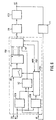
- FIG. 6 shows a phase locked loop with a digital one Phase detector PD1, a digital-to-analog converter DA, one tunable oscillator VCO and a frequency divider FT shown.
- the frequency divider FT causes one of the Frequency of the reference clock RT different output clock AT.
- the phase detector PD1 corresponds to that of FIG. 1 described phase detector.
- a computing unit MP periodically registers a counter value of the Counter Z and a sign information of the logical Gate VZ.
- the processing unit MP processes this data internally by means of a program flow in order to To generate detector characteristic according to Figure 5. Based on the processing unit MP controls the detector characteristic VCO oscillator to readjust the comparison clock VT.
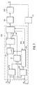
- FIG 7 is a phase locked loop with another digital phase detector PD2 shown.
- the counter value of the Counter Z and the sign information of the logical Gates VZ are here in the manner with the computing unit MP connected in terms of circuitry that the computing effort in the Computing unit MP for generating the detector characteristic not applicable.
- the sign information Vt is the same for that Sign responsible for the input data entry bit connected.
Landscapes
- Physics & Mathematics (AREA)
- General Physics & Mathematics (AREA)
- Stabilization Of Oscillater, Synchronisation, Frequency Synthesizers (AREA)
- Manipulation Of Pulses (AREA)
- Synchronisation In Digital Transmission Systems (AREA)
- Measuring Phase Differences (AREA)
- Signal Processing For Digital Recording And Reproducing (AREA)
Description
Claims (4)
- Digitaler Phasendetektor zur Gewinnung von Phaseninformationen zwischen einem Referenztakt und einem Vergleichstakt, mit ersten Mitteln (STA, STO), die aus zeitlich aufeinanderfolgenden Impulsen des Referenz- und Vergleichstakts Start- und Stopsignale generieren, mit einem Zähler (Z), der Impulse eines Zähltakts in dem Zeitfenster zwischen einem Startsignal und dem nachfolgenden Stopsignal hochzählt, wobei der Zählerwert des Zählers (Z) ein Maß für die Phasenverschiebung zwischen dem Referenztakt und dem Vergleichstakt darstellt, und mit zweiten Mitteln (VZ), die aus dem im Vergleich zum Referenztakt vor- oder nacheilenden Vergleichstakt eine Vorzeicheninformation gewinnen, dadurch gekennzeichnet, daß dritte Mittel (MP) vorhanden sind, die zu dem Zählerwert (ZW) eine Konstante hinzuaddieren und dem resultierenden Wert die Vorzeicheninformation zuordnen.
- Digitaler Phasendetektor nach Anspruch 1, dadurch gekennzeichnet, daß zur Durchführung der Addition der Konstanten eine feste Beschaltung am Dateneingang der dritten Mittel (MP) vorgesehen ist.
- Digitaler Phasendetektor nach Anspruch 1 oder 2, dadurch gekennzeichnet, daß die dritten Mittel (MP) zu dem Zählerwert eine Konstante 0,5 hinzuaddieren, indem die k Bits des Zählerwerts am Eingang der dritten Mittel (MP) um 1 Bit in Richtung des höheren Bits verschoben werden und das niedrigste Bit dieses Eingangs permanent auf Pegel "H" gelegt wird.
- Digitaler Phasendetektor nach einem der vorhergehenden Ansprüche, dadurch gekennzeichnet, daß er in einem Phasenregelkreis eingesetzt ist.
Applications Claiming Priority (3)
| Application Number | Priority Date | Filing Date | Title |
|---|---|---|---|
| DE4344867A DE4344867C1 (de) | 1993-12-29 | 1993-12-29 | Digitaler Phasendetektor |
| DE4344867 | 1993-12-29 | ||
| PCT/DE1994/001380 WO1995018384A1 (de) | 1993-12-29 | 1994-11-23 | Digitaler phasendetektor |
Publications (2)
| Publication Number | Publication Date |
|---|---|
| EP0737317A1 EP0737317A1 (de) | 1996-10-16 |
| EP0737317B1 true EP0737317B1 (de) | 1998-04-08 |
Family
ID=6506472
Family Applications (1)
| Application Number | Title | Priority Date | Filing Date |
|---|---|---|---|
| EP95901322A Expired - Lifetime EP0737317B1 (de) | 1993-12-29 | 1994-11-23 | Digitaler phasendetektor |
Country Status (12)
| Country | Link |
|---|---|
| US (1) | US5818265A (de) |
| EP (1) | EP0737317B1 (de) |
| JP (1) | JPH09507103A (de) |
| AT (1) | ATE164946T1 (de) |
| BR (1) | BR9408451A (de) |
| CZ (1) | CZ287914B6 (de) |
| DE (2) | DE4344867C1 (de) |
| DK (1) | DK0737317T3 (de) |
| ES (1) | ES2115345T3 (de) |
| FI (1) | FI962642A7 (de) |
| HU (1) | HU218125B (de) |
| WO (1) | WO1995018384A1 (de) |
Families Citing this family (12)
| Publication number | Priority date | Publication date | Assignee | Title |
|---|---|---|---|---|
| KR100190032B1 (ko) * | 1996-03-30 | 1999-06-01 | 윤종용 | Efm 데이타 복원용 클럭 발생방법 및 그 방법을 수행하는 위상동기 루프 |
| US6618775B1 (en) * | 1997-08-15 | 2003-09-09 | Micron Technology, Inc. | DSP bus monitoring apparatus and method |
| US6288574B1 (en) * | 1999-12-21 | 2001-09-11 | Xerox Corporation | Digital phase detector |
| US6407599B1 (en) | 2000-05-10 | 2002-06-18 | Eastman Kodak Company | Method and apparatus for determining a digital phase shift in a signal |
| US6868135B1 (en) | 2000-05-18 | 2005-03-15 | Eastman Kodak Company | Method and apparatus for correcting for a phase shift between a transmitter and a receiver |
| US6671652B2 (en) * | 2001-12-26 | 2003-12-30 | Hewlett-Packard Devlopment Company, L.P. | Clock skew measurement circuit on a microprocessor die |
| US7839178B2 (en) * | 2002-08-20 | 2010-11-23 | Seagate Technology Llc | High speed digital phase/frequency comparator for phase locked loops |
| JP2011120216A (ja) * | 2009-11-05 | 2011-06-16 | Rohm Co Ltd | アンテナ駆動装置 |
| US8081013B1 (en) * | 2010-07-13 | 2011-12-20 | Amlogic Co., Ltd. | Digital phase and frequency detector |
| US8618854B2 (en) | 2010-10-15 | 2013-12-31 | Qualcomm Incorporated | Adaptive clock switching to capture asynchronous data within a phase-to-digital converter |
| US8585050B2 (en) | 2011-12-06 | 2013-11-19 | Eastman Kodak Company | Combined ultrasonic-based multifeed detection system and sound-based damage detection system |
| US8781049B1 (en) | 2012-12-27 | 2014-07-15 | Intel Mobile Communications GmbH | Signal delay estimator with absolute delay amount and direction estimation |
Family Cites Families (8)
| Publication number | Priority date | Publication date | Assignee | Title |
|---|---|---|---|---|
| GB1207092A (en) * | 1969-03-19 | 1970-09-30 | Standard Telephones Cables Ltd | Phase shift detector |
| US3913028A (en) * | 1974-04-22 | 1975-10-14 | Rca Corp | Phase locked loop including an arithmetic unit |
| FR2406848A1 (fr) * | 1977-10-24 | 1979-05-18 | Sony Corp | Dispositif numerique d'asservissement de phase |
| US4246497A (en) * | 1978-09-29 | 1981-01-20 | Neil Brown Instruments Systems, Inc. | Phase measuring circuit |
| US4264866A (en) * | 1979-01-04 | 1981-04-28 | Ladislav Benes | Frequency and phase comparator |
| US4322643A (en) * | 1980-04-28 | 1982-03-30 | Rca Corporation | Digital phase comparator with improved sensitivity for small phase differences |
| US4506175A (en) * | 1982-08-18 | 1985-03-19 | Rca Corporation | Digital phase comparator circuit producing sign and magnitude outputs |
| US5180933A (en) * | 1991-11-26 | 1993-01-19 | Honeywell Inc. | Programmable digital out-of-lock detector |
-
1993
- 1993-12-29 DE DE4344867A patent/DE4344867C1/de not_active Expired - Fee Related
-
1994
- 1994-11-23 US US08/656,320 patent/US5818265A/en not_active Expired - Lifetime
- 1994-11-23 HU HU9601788A patent/HU218125B/hu not_active IP Right Cessation
- 1994-11-23 DK DK95901322T patent/DK0737317T3/da active
- 1994-11-23 CZ CZ19961865A patent/CZ287914B6/cs not_active IP Right Cessation
- 1994-11-23 AT AT95901322T patent/ATE164946T1/de not_active IP Right Cessation
- 1994-11-23 BR BR9408451A patent/BR9408451A/pt not_active IP Right Cessation
- 1994-11-23 DE DE59405666T patent/DE59405666D1/de not_active Expired - Lifetime
- 1994-11-23 EP EP95901322A patent/EP0737317B1/de not_active Expired - Lifetime
- 1994-11-23 WO PCT/DE1994/001380 patent/WO1995018384A1/de not_active Ceased
- 1994-11-23 ES ES95901322T patent/ES2115345T3/es not_active Expired - Lifetime
- 1994-11-23 JP JP7517713A patent/JPH09507103A/ja active Pending
-
1996
- 1996-06-26 FI FI962642A patent/FI962642A7/fi unknown
Also Published As
| Publication number | Publication date |
|---|---|
| EP0737317A1 (de) | 1996-10-16 |
| CZ287914B6 (cs) | 2001-03-14 |
| DE4344867C1 (de) | 1995-04-06 |
| ES2115345T3 (es) | 1998-06-16 |
| CZ186596A3 (en) | 1997-01-15 |
| US5818265A (en) | 1998-10-06 |
| FI962642A0 (fi) | 1996-06-26 |
| HU9601788D0 (en) | 1996-09-30 |
| FI962642A7 (fi) | 1996-06-26 |
| HUT74632A (en) | 1997-01-28 |
| HU218125B (hu) | 2000-06-28 |
| JPH09507103A (ja) | 1997-07-15 |
| WO1995018384A1 (de) | 1995-07-06 |
| DE59405666D1 (de) | 1998-05-14 |
| ATE164946T1 (de) | 1998-04-15 |
| DK0737317T3 (da) | 1999-01-04 |
| BR9408451A (pt) | 1997-08-05 |
Similar Documents
| Publication | Publication Date | Title |
|---|---|---|
| EP0737317B1 (de) | Digitaler phasendetektor | |
| DE19838096C2 (de) | Fraktionaler Phasenregelkreis | |
| DE68927148T2 (de) | Digitaler Phasenregelkreis | |
| DE3332152C2 (de) | ||
| DE102008062526A1 (de) | Phasenregelkreis mit adaptivem Filter für die Synchronisation eines digital gesteuerten Oszillators | |
| DE3026230C2 (de) | ||
| EP0610990B1 (de) | Digitale Phasenregelschleife | |
| EP1198889B1 (de) | Taktsignalgenerator | |
| DE2836723A1 (de) | Zeitsteuerschaltung | |
| DE69321008T2 (de) | Frequenzsynthetisierer mit gebrochenem Teilverhältnis mit Digitalfehlerkorrektion | |
| DE4004195C2 (de) | Schaltungsanordnung zur Erzeugung eines mit einem Referenzsignal verkoppelten Signals | |
| DE3826006C1 (de) | ||
| EP0729583B1 (de) | Phasenmessvorrichtung | |
| DE3511698C2 (de) | ||
| EP0264035B1 (de) | Phasendiskriminator, insbesondere für eine PLL-Schaltung | |
| DE2735053C3 (de) | Digitaler Phasenregelkreis | |
| DE69029442T2 (de) | Zeitintervall-Triggerung und Hardware Erzeugung von Histogramm | |
| DE2613930C3 (de) | Digitaler Phasenregelkreis | |
| DE102006021821A1 (de) | Einstellbarer Zeitakkumulator | |
| DE69419150T2 (de) | Digital gesteuerter oszillator und digitale pll-schaltung | |
| DE102009052481B4 (de) | Phasenregelkreis | |
| DE60219156T2 (de) | Verfahren und Einrichtung für die parallele Synchronisation von mehreren seriellen Datenströmen | |
| DE102008064063A1 (de) | Steuersignalerzeugungsschaltung zur Einstellung eines Periodenwerts eines erzeugten Taktsignals als die Periode eines Referenzsignals, multipliziert mit oder dividiert durch eine beliebige reelle Zahl | |
| DE2139404B2 (de) | Verfahren zur Synchronisierung | |
| DE19513795C1 (de) | Schaltungsanordnung zur digitalen Phasendifferenzmessung |
Legal Events
| Date | Code | Title | Description |
|---|---|---|---|
| PUAI | Public reference made under article 153(3) epc to a published international application that has entered the european phase |
Free format text: ORIGINAL CODE: 0009012 |
|
| 17P | Request for examination filed |
Effective date: 19960729 |
|
| AK | Designated contracting states |
Kind code of ref document: A1 Designated state(s): AT CH DE DK ES FR GB IT LI PT SE |
|
| GRAG | Despatch of communication of intention to grant |
Free format text: ORIGINAL CODE: EPIDOS AGRA |
|
| 17Q | First examination report despatched |
Effective date: 19970729 |
|
| GRAG | Despatch of communication of intention to grant |
Free format text: ORIGINAL CODE: EPIDOS AGRA |
|
| GRAH | Despatch of communication of intention to grant a patent |
Free format text: ORIGINAL CODE: EPIDOS IGRA |
|
| GRAH | Despatch of communication of intention to grant a patent |
Free format text: ORIGINAL CODE: EPIDOS IGRA |
|
| GRAA | (expected) grant |
Free format text: ORIGINAL CODE: 0009210 |
|
| AK | Designated contracting states |
Kind code of ref document: B1 Designated state(s): AT CH DE DK ES FR GB IT LI PT SE |
|
| REF | Corresponds to: |
Ref document number: 164946 Country of ref document: AT Date of ref document: 19980415 Kind code of ref document: T |
|
| REG | Reference to a national code |
Ref country code: CH Ref legal event code: NV Representative=s name: SCINTILLA AG, DIREKTION Ref country code: CH Ref legal event code: EP |
|
| ET | Fr: translation filed | ||
| REF | Corresponds to: |
Ref document number: 59405666 Country of ref document: DE Date of ref document: 19980514 |
|
| REG | Reference to a national code |
Ref country code: ES Ref legal event code: FG2A Ref document number: 2115345 Country of ref document: ES Kind code of ref document: T3 |
|
| ITF | It: translation for a ep patent filed | ||
| GBT | Gb: translation of ep patent filed (gb section 77(6)(a)/1977) |
Effective date: 19980610 |
|
| PGFP | Annual fee paid to national office [announced via postgrant information from national office to epo] |
Ref country code: PT Payment date: 19981029 Year of fee payment: 5 |
|
| REG | Reference to a national code |
Ref country code: PT Ref legal event code: SC4A Free format text: AVAILABILITY OF NATIONAL TRANSLATION Effective date: 19980707 |
|
| PGFP | Annual fee paid to national office [announced via postgrant information from national office to epo] |
Ref country code: DK Payment date: 19981204 Year of fee payment: 5 |
|
| REG | Reference to a national code |
Ref country code: DK Ref legal event code: T3 |
|
| PLBE | No opposition filed within time limit |
Free format text: ORIGINAL CODE: 0009261 |
|
| STAA | Information on the status of an ep patent application or granted ep patent |
Free format text: STATUS: NO OPPOSITION FILED WITHIN TIME LIMIT |
|
| 26N | No opposition filed | ||
| PG25 | Lapsed in a contracting state [announced via postgrant information from national office to epo] |
Ref country code: DK Free format text: LAPSE BECAUSE OF NON-PAYMENT OF DUE FEES Effective date: 19991123 |
|
| PG25 | Lapsed in a contracting state [announced via postgrant information from national office to epo] |
Ref country code: PT Free format text: LAPSE BECAUSE OF NON-PAYMENT OF DUE FEES Effective date: 20000531 |
|
| REG | Reference to a national code |
Ref country code: DK Ref legal event code: EBP |
|
| REG | Reference to a national code |
Ref country code: PT Ref legal event code: MM4A Free format text: LAPSE DUE TO NON-PAYMENT OF FEES Effective date: 20000531 |
|
| PGFP | Annual fee paid to national office [announced via postgrant information from national office to epo] |
Ref country code: AT Payment date: 20001113 Year of fee payment: 7 |
|
| PGFP | Annual fee paid to national office [announced via postgrant information from national office to epo] |
Ref country code: CH Payment date: 20001128 Year of fee payment: 7 |
|
| PG25 | Lapsed in a contracting state [announced via postgrant information from national office to epo] |
Ref country code: AT Free format text: LAPSE BECAUSE OF NON-PAYMENT OF DUE FEES Effective date: 20011123 |
|
| PG25 | Lapsed in a contracting state [announced via postgrant information from national office to epo] |
Ref country code: LI Free format text: LAPSE BECAUSE OF NON-PAYMENT OF DUE FEES Effective date: 20011130 Ref country code: CH Free format text: LAPSE BECAUSE OF NON-PAYMENT OF DUE FEES Effective date: 20011130 |
|
| REG | Reference to a national code |
Ref country code: GB Ref legal event code: IF02 |
|
| REG | Reference to a national code |
Ref country code: CH Ref legal event code: PL |
|
| PGFP | Annual fee paid to national office [announced via postgrant information from national office to epo] |
Ref country code: ES Payment date: 20021127 Year of fee payment: 9 |
|
| REG | Reference to a national code |
Ref country code: GB Ref legal event code: 732E |
|
| PG25 | Lapsed in a contracting state [announced via postgrant information from national office to epo] |
Ref country code: ES Free format text: LAPSE BECAUSE OF NON-PAYMENT OF DUE FEES Effective date: 20031124 |
|
| REG | Reference to a national code |
Ref country code: FR Ref legal event code: TP |
|
| REG | Reference to a national code |
Ref country code: ES Ref legal event code: FD2A Effective date: 20031124 |
|
| REG | Reference to a national code |
Ref country code: GB Ref legal event code: 732E |
|
| REG | Reference to a national code |
Ref country code: FR Ref legal event code: TP |
|
| GBPC | Gb: european patent ceased through non-payment of renewal fee |
Effective date: 20061123 |
|
| PG25 | Lapsed in a contracting state [announced via postgrant information from national office to epo] |
Ref country code: GB Free format text: LAPSE BECAUSE OF NON-PAYMENT OF DUE FEES Effective date: 20061123 |
|
| REG | Reference to a national code |
Ref country code: GB Ref legal event code: 728V |
|
| PGFP | Annual fee paid to national office [announced via postgrant information from national office to epo] |
Ref country code: IT Payment date: 20071129 Year of fee payment: 14 |
|
| PGFP | Annual fee paid to national office [announced via postgrant information from national office to epo] |
Ref country code: SE Payment date: 20071128 Year of fee payment: 14 |
|
| REG | Reference to a national code |
Ref country code: GB Ref legal event code: S28 Effective date: 20080522 |
|
| EUG | Se: european patent has lapsed | ||
| PG25 | Lapsed in a contracting state [announced via postgrant information from national office to epo] |
Ref country code: IT Free format text: LAPSE BECAUSE OF NON-PAYMENT OF DUE FEES Effective date: 20081123 |
|
| PG25 | Lapsed in a contracting state [announced via postgrant information from national office to epo] |
Ref country code: SE Free format text: LAPSE BECAUSE OF NON-PAYMENT OF DUE FEES Effective date: 20081124 |
|
| PGFP | Annual fee paid to national office [announced via postgrant information from national office to epo] |
Ref country code: FR Payment date: 20121206 Year of fee payment: 19 Ref country code: DE Payment date: 20121128 Year of fee payment: 19 |
|
| PGFP | Annual fee paid to national office [announced via postgrant information from national office to epo] |
Ref country code: GB Payment date: 20121126 Year of fee payment: 19 |
|
| REG | Reference to a national code |
Ref country code: DE Ref legal event code: R119 Ref document number: 59405666 Country of ref document: DE |
|
| GBPC | Gb: european patent ceased through non-payment of renewal fee |
Effective date: 20131123 |
|
| REG | Reference to a national code |
Ref country code: FR Ref legal event code: ST Effective date: 20140731 |
|
| PG25 | Lapsed in a contracting state [announced via postgrant information from national office to epo] |
Ref country code: DE Free format text: LAPSE BECAUSE OF NON-PAYMENT OF DUE FEES Effective date: 20140603 |
|
| REG | Reference to a national code |
Ref country code: DE Ref legal event code: R119 Ref document number: 59405666 Country of ref document: DE Effective date: 20140603 |
|
| PG25 | Lapsed in a contracting state [announced via postgrant information from national office to epo] |
Ref country code: GB Free format text: LAPSE BECAUSE OF NON-PAYMENT OF DUE FEES Effective date: 20131123 Ref country code: FR Free format text: LAPSE BECAUSE OF NON-PAYMENT OF DUE FEES Effective date: 20131202 |