EP0738003A2 - Méthode pour la formation d'une couche en oxyde de silicium pour des dispositifs semi-conducteurs par dépÔt chimique en phase vapeur à basse pression (LPCVD) - Google Patents
Méthode pour la formation d'une couche en oxyde de silicium pour des dispositifs semi-conducteurs par dépÔt chimique en phase vapeur à basse pression (LPCVD) Download PDFInfo
- Publication number
- EP0738003A2 EP0738003A2 EP96105727A EP96105727A EP0738003A2 EP 0738003 A2 EP0738003 A2 EP 0738003A2 EP 96105727 A EP96105727 A EP 96105727A EP 96105727 A EP96105727 A EP 96105727A EP 0738003 A2 EP0738003 A2 EP 0738003A2
- Authority
- EP
- European Patent Office
- Prior art keywords
- silicon oxide
- film
- gas
- depositing
- forming
- Prior art date
- Legal status (The legal status is an assumption and is not a legal conclusion. Google has not performed a legal analysis and makes no representation as to the accuracy of the status listed.)
- Withdrawn
Links
Images




Classifications
-
- H—ELECTRICITY
- H10—SEMICONDUCTOR DEVICES; ELECTRIC SOLID-STATE DEVICES NOT OTHERWISE PROVIDED FOR
- H10D—INORGANIC ELECTRIC SEMICONDUCTOR DEVICES
- H10D30/00—Field-effect transistors [FET]
- H10D30/01—Manufacture or treatment
- H10D30/021—Manufacture or treatment of FETs having insulated gates [IGFET]
- H10D30/031—Manufacture or treatment of FETs having insulated gates [IGFET] of thin-film transistors [TFT]
- H10D30/0312—Manufacture or treatment of FETs having insulated gates [IGFET] of thin-film transistors [TFT] characterised by the gate electrodes
- H10D30/0316—Manufacture or treatment of FETs having insulated gates [IGFET] of thin-film transistors [TFT] characterised by the gate electrodes of lateral bottom-gate TFTs comprising only a single gate
-
- H—ELECTRICITY
- H10—SEMICONDUCTOR DEVICES; ELECTRIC SOLID-STATE DEVICES NOT OTHERWISE PROVIDED FOR
- H10P—GENERIC PROCESSES OR APPARATUS FOR THE MANUFACTURE OR TREATMENT OF DEVICES COVERED BY CLASS H10
- H10P14/00—Formation of materials, e.g. in the shape of layers or pillars
- H10P14/60—Formation of materials, e.g. in the shape of layers or pillars of insulating materials
- H10P14/63—Formation of materials, e.g. in the shape of layers or pillars of insulating materials characterised by the formation processes
- H10P14/6326—Deposition processes
- H10P14/6328—Deposition from the gas or vapour phase
- H10P14/6334—Deposition from the gas or vapour phase using decomposition or reaction of gaseous or vapour phase compounds, i.e. chemical vapour deposition
- H10P14/6338—Deposition from the gas or vapour phase using decomposition or reaction of gaseous or vapour phase compounds, i.e. chemical vapour deposition the reactions being activated by other means than plasma or thermal, e.g. photo-CVD
-
- C—CHEMISTRY; METALLURGY
- C23—COATING METALLIC MATERIAL; COATING MATERIAL WITH METALLIC MATERIAL; CHEMICAL SURFACE TREATMENT; DIFFUSION TREATMENT OF METALLIC MATERIAL; COATING BY VACUUM EVAPORATION, BY SPUTTERING, BY ION IMPLANTATION OR BY CHEMICAL VAPOUR DEPOSITION, IN GENERAL; INHIBITING CORROSION OF METALLIC MATERIAL OR INCRUSTATION IN GENERAL
- C23C—COATING METALLIC MATERIAL; COATING MATERIAL WITH METALLIC MATERIAL; SURFACE TREATMENT OF METALLIC MATERIAL BY DIFFUSION INTO THE SURFACE, BY CHEMICAL CONVERSION OR SUBSTITUTION; COATING BY VACUUM EVAPORATION, BY SPUTTERING, BY ION IMPLANTATION OR BY CHEMICAL VAPOUR DEPOSITION, IN GENERAL
- C23C16/00—Chemical coating by decomposition of gaseous compounds, without leaving reaction products of surface material in the coating, i.e. chemical vapour deposition [CVD] processes
- C23C16/22—Chemical coating by decomposition of gaseous compounds, without leaving reaction products of surface material in the coating, i.e. chemical vapour deposition [CVD] processes characterised by the deposition of inorganic material, other than metallic material
- C23C16/30—Deposition of compounds, mixtures or solid solutions, e.g. borides, carbides, nitrides
- C23C16/40—Oxides
- C23C16/401—Oxides containing silicon
- C23C16/402—Silicon dioxide
-
- H—ELECTRICITY
- H10—SEMICONDUCTOR DEVICES; ELECTRIC SOLID-STATE DEVICES NOT OTHERWISE PROVIDED FOR
- H10D—INORGANIC ELECTRIC SEMICONDUCTOR DEVICES
- H10D30/00—Field-effect transistors [FET]
- H10D30/01—Manufacture or treatment
- H10D30/021—Manufacture or treatment of FETs having insulated gates [IGFET]
- H10D30/031—Manufacture or treatment of FETs having insulated gates [IGFET] of thin-film transistors [TFT]
- H10D30/0321—Manufacture or treatment of FETs having insulated gates [IGFET] of thin-film transistors [TFT] comprising silicon, e.g. amorphous silicon or polysilicon
-
- H—ELECTRICITY
- H10—SEMICONDUCTOR DEVICES; ELECTRIC SOLID-STATE DEVICES NOT OTHERWISE PROVIDED FOR
- H10D—INORGANIC ELECTRIC SEMICONDUCTOR DEVICES
- H10D30/00—Field-effect transistors [FET]
- H10D30/01—Manufacture or treatment
- H10D30/021—Manufacture or treatment of FETs having insulated gates [IGFET]
- H10D30/0411—Manufacture or treatment of FETs having insulated gates [IGFET] of FETs having floating gates
-
- H—ELECTRICITY
- H10—SEMICONDUCTOR DEVICES; ELECTRIC SOLID-STATE DEVICES NOT OTHERWISE PROVIDED FOR
- H10D—INORGANIC ELECTRIC SEMICONDUCTOR DEVICES
- H10D64/00—Electrodes of devices having potential barriers
- H10D64/01—Manufacture or treatment
- H10D64/013—Manufacture or treatment of electrodes having a conductor capacitively coupled to a semiconductor by an insulator
-
- H—ELECTRICITY
- H10—SEMICONDUCTOR DEVICES; ELECTRIC SOLID-STATE DEVICES NOT OTHERWISE PROVIDED FOR
- H10D—INORGANIC ELECTRIC SEMICONDUCTOR DEVICES
- H10D84/00—Integrated devices formed in or on semiconductor substrates that comprise only semiconducting layers, e.g. on Si wafers or on GaAs-on-Si wafers
- H10D84/01—Manufacture or treatment
- H10D84/0123—Integrating together multiple components covered by H10D12/00 or H10D30/00, e.g. integrating multiple IGBTs
- H10D84/0126—Integrating together multiple components covered by H10D12/00 or H10D30/00, e.g. integrating multiple IGBTs the components including insulated gates, e.g. IGFETs
- H10D84/0165—Integrating together multiple components covered by H10D12/00 or H10D30/00, e.g. integrating multiple IGBTs the components including insulated gates, e.g. IGFETs the components including complementary IGFETs, e.g. CMOS devices
- H10D84/0186—Manufacturing their interconnections or electrodes, e.g. source or drain electrodes
-
- H—ELECTRICITY
- H10—SEMICONDUCTOR DEVICES; ELECTRIC SOLID-STATE DEVICES NOT OTHERWISE PROVIDED FOR
- H10D—INORGANIC ELECTRIC SEMICONDUCTOR DEVICES
- H10D84/00—Integrated devices formed in or on semiconductor substrates that comprise only semiconducting layers, e.g. on Si wafers or on GaAs-on-Si wafers
- H10D84/01—Manufacture or treatment
- H10D84/0123—Integrating together multiple components covered by H10D12/00 or H10D30/00, e.g. integrating multiple IGBTs
- H10D84/0126—Integrating together multiple components covered by H10D12/00 or H10D30/00, e.g. integrating multiple IGBTs the components including insulated gates, e.g. IGFETs
- H10D84/0165—Integrating together multiple components covered by H10D12/00 or H10D30/00, e.g. integrating multiple IGBTs the components including insulated gates, e.g. IGFETs the components including complementary IGFETs, e.g. CMOS devices
- H10D84/0188—Manufacturing their isolation regions
-
- H—ELECTRICITY
- H10—SEMICONDUCTOR DEVICES; ELECTRIC SOLID-STATE DEVICES NOT OTHERWISE PROVIDED FOR
- H10D—INORGANIC ELECTRIC SEMICONDUCTOR DEVICES
- H10D84/00—Integrated devices formed in or on semiconductor substrates that comprise only semiconducting layers, e.g. on Si wafers or on GaAs-on-Si wafers
- H10D84/01—Manufacture or treatment
- H10D84/02—Manufacture or treatment characterised by using material-based technologies
- H10D84/03—Manufacture or treatment characterised by using material-based technologies using Group IV technology, e.g. silicon technology or silicon-carbide [SiC] technology
- H10D84/038—Manufacture or treatment characterised by using material-based technologies using Group IV technology, e.g. silicon technology or silicon-carbide [SiC] technology using silicon technology, e.g. SiGe
-
- H—ELECTRICITY
- H10—SEMICONDUCTOR DEVICES; ELECTRIC SOLID-STATE DEVICES NOT OTHERWISE PROVIDED FOR
- H10D—INORGANIC ELECTRIC SEMICONDUCTOR DEVICES
- H10D86/00—Integrated devices formed in or on insulating or conducting substrates, e.g. formed in silicon-on-insulator [SOI] substrates or on stainless steel or glass substrates
- H10D86/01—Manufacture or treatment
-
- H—ELECTRICITY
- H10—SEMICONDUCTOR DEVICES; ELECTRIC SOLID-STATE DEVICES NOT OTHERWISE PROVIDED FOR
- H10P—GENERIC PROCESSES OR APPARATUS FOR THE MANUFACTURE OR TREATMENT OF DEVICES COVERED BY CLASS H10
- H10P14/00—Formation of materials, e.g. in the shape of layers or pillars
- H10P14/60—Formation of materials, e.g. in the shape of layers or pillars of insulating materials
- H10P14/63—Formation of materials, e.g. in the shape of layers or pillars of insulating materials characterised by the formation processes
- H10P14/6326—Deposition processes
- H10P14/6328—Deposition from the gas or vapour phase
- H10P14/6334—Deposition from the gas or vapour phase using decomposition or reaction of gaseous or vapour phase compounds, i.e. chemical vapour deposition
-
- H—ELECTRICITY
- H10—SEMICONDUCTOR DEVICES; ELECTRIC SOLID-STATE DEVICES NOT OTHERWISE PROVIDED FOR
- H10P—GENERIC PROCESSES OR APPARATUS FOR THE MANUFACTURE OR TREATMENT OF DEVICES COVERED BY CLASS H10
- H10P14/00—Formation of materials, e.g. in the shape of layers or pillars
- H10P14/60—Formation of materials, e.g. in the shape of layers or pillars of insulating materials
- H10P14/66—Formation of materials, e.g. in the shape of layers or pillars of insulating materials characterised by the type of materials
- H10P14/668—Formation of materials, e.g. in the shape of layers or pillars of insulating materials characterised by the type of materials the materials being characterised by the deposition precursor materials
- H10P14/6681—Formation of materials, e.g. in the shape of layers or pillars of insulating materials characterised by the type of materials the materials being characterised by the deposition precursor materials the precursor containing a compound comprising Si
- H10P14/6682—Formation of materials, e.g. in the shape of layers or pillars of insulating materials characterised by the type of materials the materials being characterised by the deposition precursor materials the precursor containing a compound comprising Si the compound being a silane, e.g. disilane, methylsilane or chlorosilane
-
- H—ELECTRICITY
- H10—SEMICONDUCTOR DEVICES; ELECTRIC SOLID-STATE DEVICES NOT OTHERWISE PROVIDED FOR
- H10P—GENERIC PROCESSES OR APPARATUS FOR THE MANUFACTURE OR TREATMENT OF DEVICES COVERED BY CLASS H10
- H10P14/00—Formation of materials, e.g. in the shape of layers or pillars
- H10P14/60—Formation of materials, e.g. in the shape of layers or pillars of insulating materials
- H10P14/69—Inorganic materials
- H10P14/692—Inorganic materials composed of oxides, glassy oxides or oxide-based glasses
- H10P14/6921—Inorganic materials composed of oxides, glassy oxides or oxide-based glasses containing silicon
- H10P14/69215—Inorganic materials composed of oxides, glassy oxides or oxide-based glasses containing silicon the material being a silicon oxide, e.g. SiO2
-
- H—ELECTRICITY
- H10—SEMICONDUCTOR DEVICES; ELECTRIC SOLID-STATE DEVICES NOT OTHERWISE PROVIDED FOR
- H10W—GENERIC PACKAGES, INTERCONNECTIONS, CONNECTORS OR OTHER CONSTRUCTIONAL DETAILS OF DEVICES COVERED BY CLASS H10
- H10W20/00—Interconnections in chips, wafers or substrates
- H10W20/01—Manufacture or treatment
- H10W20/071—Manufacture or treatment of dielectric parts thereof
-
- H—ELECTRICITY
- H10—SEMICONDUCTOR DEVICES; ELECTRIC SOLID-STATE DEVICES NOT OTHERWISE PROVIDED FOR
- H10W—GENERIC PACKAGES, INTERCONNECTIONS, CONNECTORS OR OTHER CONSTRUCTIONAL DETAILS OF DEVICES COVERED BY CLASS H10
- H10W20/00—Interconnections in chips, wafers or substrates
- H10W20/01—Manufacture or treatment
- H10W20/071—Manufacture or treatment of dielectric parts thereof
- H10W20/074—Manufacture or treatment of dielectric parts thereof of dielectric parts comprising thin functional dielectric layers, e.g. dielectric etch-stop, barrier, capping or liner layers
- H10W20/077—Manufacture or treatment of dielectric parts thereof of dielectric parts comprising thin functional dielectric layers, e.g. dielectric etch-stop, barrier, capping or liner layers on sidewalls or on top surfaces of conductors
Definitions
- the present invention relates to a method of forming a silicon oxide film which is used in a semiconductor device such as a VLSI by utilizing a low pressure CVD (chemical vapor deposition) method, and also to a method of manufacturing a semiconductor device using the method of forming a silicon oxide film.
- a semiconductor device such as a VLSI by utilizing a low pressure CVD (chemical vapor deposition) method
- CVD chemical vapor deposition
- a method of forming a silicon oxide film which is used in a semiconductor device such as a VLSI, a low pressure CVD method, an atmospheric pressure CVD method and a plasma CVD method are known.
- a silicon oxide film which is formed by a low pressure CVD method is superior to a silicon oxide film which is formed by an atmospheric pressure CVD method, a plasma CVD method or the like in terms of density and purity.
- a silicon oxide film which is formed by a low pressure CVD method as an insulating film for a gate electrode or as a side-wall for a gate electrode and the like.
- Silicon oxide films are classified into LTO (Low Temperature Oxide) films which are deposited at a low temperature about 400°C by an atmospheric pressure CVD method, a plasma CVD method or the like and HTO (High Temperature Oxide) films which are deposited at a high temperature from 700 to 850°C by a low pressure CVD method.
- LTO Low Temperature Oxide
- HTO High Temperature Oxide
- TEOS tetraethoxysilicate
- TEOS TE oxide film
- this method is superior to the method which uses silane gas, in terms of a decrease in a temperature during processes and ease of mass production.
- a low pressure CVD method using TEOS is often used in manufacturing processes for manufacturing a semiconductor device such as a VLSI.
- a low pressure CVD method using TEOS has a problem that the yield is greatly reduced and a cost for maintaining a device is increased.
- a low pressure CVD method using silane gas is preferred to form a silicon oxide film during manufacturing processes for manufacturing a semiconductor device such as a VLSI.
- a deposition temperature is conventionally 820°C or higher since a deposition speed is slow in a low pressure CVD method using silane gas
- a deposition temperature is 820°C or higher
- a deposition temperature is set at 800°C or at a lower temperature in a conventional low pressure CVD method using silane gas, a deposition time must be increased. Due to this constraint, it is still impossible to accurately control a diffusion profile of an impurity, which is a second problem.
- a first object of the present invention is to form a silicon oxide film with a uniform thickness
- a second object of the present invention is to accurately control diffusion of an impurity in a semiconductor substrate.
- a first method of forming a silicon oxide film according to the present invention comprises a silicon oxide film depositing step of depositing a silicon oxide film by a low pressure CVD method in which silane gas and nitrous oxide gas are used as principal materials, and the silicon oxide film depositing step is performed under a deposition condition that a deposition temperature is 800°C or lower and a gas flow rate of the principal materials is 0.018 liter/min or smaller per 1 liter of capacity of a reaction chamber under a standard condition of 25°C at one atmospheric pressure.
- the uniformness of the film thickness of a resultant silicon oxide film reaches a limit of a tolerance range. Since collision between reaction products (deposits) becomes less frequent as the deposition temperature becomes lower than 800°C, the uniformness of the film thickness of a silicon oxide film is improved. If the deposition temperature is equal to or lower than 800°C, the uniformness of the film thickness of a silicon oxide film stays within the tolerance range.
- the gas flow rate of the principal materials becomes smaller than 0.018 liter/min per 1 liter of capacity of the reaction chamber under the standard condition, a flow of gas within the reaction chamber becomes more like a laminar flow, which makes it difficult for the gas to swirl between wafers. Since this improves the uniformness of the film thickness of a silicon oxide film which is deposited on a wafer, if the gas flow rate of the principal materials is 0.018 liter/min or smaller, the uniformness of the film thickness of the silicon oxide film stays within the tolerance range. Hence, the uniformness of the film thickness of the silicon oxide film which is obtained is improved.
- the deposition condition preferably includes a condition which causes a gas pressure of the principal materials to become equal to or smaller than 170 Pa. This ensures that the uniformness of the film thickness of a silicon oxide film which is obtained stays within the tolerance range of 4% or smaller.
- the deposition condition preferably includes a condition which causes a gas pressure of the principal materials to become equal to or smaller than 125 Pa. This ensures that the uniformness of the film thickness of a silicon oxide film obtained is ideally 3% or smaller.
- a second method of forming a silicon oxide film according to the present invention comprises a silicon oxide film depositing step of depositing a silicon oxide film by a low pressure CVD method in which silane gas and nitrous oxide gas are used as principal materials, and the silicon oxide film depositing step is performed under a deposition condition that a deposition temperature is 800°C or lower and a gas pressure of the principal materials is 100 Pa or larger.
- the deposition temperature is 800°C or lower and the gas pressure of the principal materials is 100 Pa or larger, it is possible to steadily suppress diffusion of an impurity, and therefore, it is possible to satisfy a standard which is usually used in manufacturing processes for manufacturing a VLSI that an effective gate length is 80% or longer of a designed gate length. Since the effective gate length is the most sensitive to an adverse effect due to impurity diffusion during VLSI manufacturing processes, if the standard requiring the effective gate length to be 80% or longer of the designed gate length is satisfied, a silicon oxide film is sufficiently appropriate as an insulating film such as an insulating film which is disposed between a control gate and a floating gate of a flash memory. Hence, it is possible to deposit a silicon oxide film while steadily suppressing diffusion of an impurity.
- the deposition temperature is preferably from 780°C to 800°C and the gas pressure of the principal materials is preferably 100 Pa or larger. This makes it possible to steadily suppress diffusion of an impurity so that the effective gate length/the designed gate length becomes 80% or smaller.
- the deposition temperature is preferably from 740°C to 800°C and the gas pressure of the principal materials is preferably 125 Pa or larger. This makes it possible to steadily suppress diffusion of an impurity so that the effective gate length/the designed gate length becomes 80% or smaller.
- the first or the second method of forming a silicon oxide film it is possible to improve the yield of manufacturing a semiconductor device without modifying a low pressure CVD system.
- a first method of manufacturing a semiconductor device comprises: a gate electrode forming step of forming a gate electrode on a semiconductor substrate in which an impurity-lightly-doped region is formed; a side-wall forming step of forming a side-wall of a silicon oxide film on the semiconductor substrate and at a side surface of the gate electrode; and a step of forming an impurity-heavily-doped region by implanting an impurity into the semiconductor substrate while using the gate electrode and the side-wall as a mask, wherein the side-wall forming step includes a step of forming the silicon oxide film by a low pressure CVD method in which silane gas and nitrous oxide gas are used as principal materials, under a deposition condition that a deposition temperature is 800°C or lower and a gas pressure of the principal materials is 100 Pa or larger.
- the first method of manufacturing a semiconductor device due to an effect which is similar to that obtained in the second method of forming a silicon oxide film, it is possible to suppress diffusion of an impurity in the impurity-lightly-doped region which is formed in the semiconductor substrate during deposition of the silicon oxide film at the side-wall forming step. Hence, it is possible to improve a characteristic of a semiconductor device which has a LDD structure.
- a second method of manufacturing a semiconductor device comprises: a wiring layer forming step of forming a wiring layer on a semiconductor substrate which is doped with an impurity; and an insulating film depositing step of depositing an insulating film of a silicon oxide film on the wiring layer, wherein the insulating film depositing step includes a step of forming the silicon oxide film by a low pressure CVD method in which silane gas and nitrous oxide gas are used as principal materials, under a deposition condition that a deposition temperature is 800°C or lower and a gas pressure of the principal materials is 100 Pa or larger.
- the second method of manufacturing a semiconductor device due to the effect which is similar to that obtained in the second method of forming a silicon oxide film, since it is possible to suppress diffusion of an impurity which is doped in the semiconductor substrate at the step of forming the insulating film of the silicon oxide layer on the wiring layer, it is possible to improve a characteristic of the semiconductor device.
- a third method of manufacturing a semiconductor device comprises: an insulating film depositing step of depositing an insulating film of a silicon oxide film on a semiconductor substrate which is doped with an impurity; a conductive film depositing step of depositing a conductive film on the insulating film; and an etching step of etching the conductive film using the insulating film as an etching stopper, wherein the insulating film depositing step includes a step of forming the silicon oxide film by a low pressure CVD method in which silane gas and nitrous oxide gas are used as principal materials, under a deposition condition that a deposition temperature is 800°C or lower and a gas pressure of the principal materials is 100 Pa or larger.
- the third method of manufacturing a semiconductor device due to the effect which is similar to that obtained in the second method of forming a silicon oxide film, since it is possible to suppress diffusion of an impurity which is doped in the semiconductor substrate at the step of forming the insulating film of the silicon oxide film which serves as an etching stopper during etching of the conductive film, it is possible to improve a characteristic of the semiconductor device.
- a fourth method of manufacturing a semiconductor device comprises: a first conductive film depositing step of depositing a first conductive film which serves as a floating gate on a semiconductor substrate which is doped with an impurity; an insulating film depositing step of depositing an insulating film of a silicon oxide film on the first conductive film; and a second conductive film depositing step of depositing a second conductive film which serves as a control gate on the insulating film, wherein the insulating film depositing step includes a step of forming the silicon oxide film by a low pressure CVD method in which silane gas and nitrous oxide gas are used as principal materials, under a deposition condition that a deposition temperature is 800°C or lower and a gas pressure of the principal materials is 100 Pa or larger.
- the fourth method of manufacturing a semiconductor device due to the effect which is similar to that obtained in the second method of forming a silicon oxide film, it is possible to suppress diffusion of an impurity which is doped in the semiconductor substrate at the step of forming the insulating layer of the silicon oxide film which is disposed between the floating gate and the control gate.
- the first conductive film is made of polysilicon, since it is possible to suppress growth of particles of polysilicon during deposition of the silicon oxide film, it is possible to lessen defects in the insulating film which contacts with the first conductive film and mechanical stress which is applied upon the insulating film. Hence, it is possible to improve a characteristic of the semiconductor device such as a flash memory.
- a fifth method of manufacturing a semiconductor device comprises: a first conductive film depositing step of depositing a first conductive film which serves as a floating gate on a semiconductor substrate which is doped with an impurity; an insulating film depositing step of depositing an insulating film of a silicon oxide film on the first conductive film; and a second conductive film depositing step of depositing a second conductive film which serves as a control gate on the insulating film, wherein the insulating film depositing step includes a step of forming the silicon oxide film by a low pressure CVD method in which silane gas and nitrous oxide gas are used as principal materials, under a deposition condition that a deposition temperature is 800°C or lower and a gas flow rate of the principal materials is 0.018 liter/min or smaller per 1 liter of capacity of a reaction chamber under a standard condition of 25°C at one atmospheric pressure.
- the fifth method of manufacturing a semiconductor device due to the effect which is similar to that obtained in the first method of forming a silicon oxide film, it is possible to suppress a variation in the uniformness of the film thickness of the insulating film of the silicon oxide film which is disposed between the floating gate and the control gate. Hence, it is possible to improve a characteristic of the semiconductor device such as a flash memory.
- a sixth method of manufacturing a semiconductor device comprises: an insulating film depositing step of depositing an insulating film of a silicon oxide film on an ITO substrate; and a conductive film depositing step of depositing a conductive film which serves as a source/drain region on the insulating film, wherein the insulating film depositing step includes a step of forming the silicon oxide film by a low pressure CVD method in which silane gas and nitrous oxide gas are used as principal materials, under a deposition condition that a deposition temperature is 800°C or lower and a gas pressure of the principal materials is 100 Pa or larger.
- the sixth method of manufacturing a semiconductor device it is possible to reduce thermal damage to the ITO substrate at the step of depositing the insulating film of the silicon oxide film on the ITO substrate. Hence, it is possible to enhance a characteristic of a TFT which is formed on the ITO substrate.
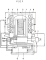
- Fig. 1 shows a structure of the low pressure CVD apparatus.
- denoted at 1 is a wafer support board for holding a plurality of wafers in a horizontal state
- denoted at 2 is an inner tube which serves as a reaction chamber for storing the wafer support board 1
- denoted at 3 is an outer tube covering the inner tube 2
- denoted at 4 is a heater which is disposed externally to the outer tube 3
- denoted at 5 is a gas introduction pipe for introducing material gas into the inner tube 2
- denoted at 6 is a mass flow controller for controlling a flow rate of gas which is introduced through the gas introduction pipe 5
- denoted at 7 is exhausting means for exhausting gas or the like from the inner tube 2
- denoted at 8 is an external thermocouple
- denoted at 9 is an internal thermocouple
- Silane gas (SiH 4 ) and nitrous oxide gas (N 2 O) which are used as principal material gas are introduced into the inner tube 2 through the gas introduction pipe 5, so that silicon oxide films are formed on the wafers which are held by the wafer support board 1.
- the material gas within the inner tube 2 and nitrogen, vapor, hydrogen and the like which are generated during reaction are discharged outside by the exhausting means 7 through the outer tube 3.
- the external thermocouple 8, the internal thermocouple 9, the pressure gauge 10 and the mass flow controller 6 measure a temperature, a gas pressure and a gas flow rate within the inner tube 2.
- the control means 11 compares the measurement with a set value to yield a deviation, and controls electric power to the heater 4, the exhaust volume of the exhausting means 7, the opening degree of a valve of the mass flow controller 6 and the like so that set values are maintained.
- the first preferred embodiment is related to a method of forming a silicon oxide film by a low pressure CVD method in which silane gas and nitrous oxide gas are used as principal materials.
- the first preferred embodiment sets a deposition condition for depositing a silicon oxide film so that a deposition temperature is 800°C or lower and a gas flow rate of the principal materials is 0.018 liter/min or smaller per 1 liter of capacity of a reaction chamber under a standard condition of 25°C at one atmospheric pressure.
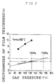
- Fig. 2 shows a relationship between a gas pressure within a reaction chamber (Pa) and the uniformness of a film thickness (%), using the flow rate of the principal material gas as a parameter.
- ⁇ expresses a case where the gas flow rate of the principal material gas is 0.018 liter/min per 1 liter of capacity of a reaction chamber under the standard condition of 25°C at one atmospheric pressure
- ⁇ expresses a case where the gas flow rate of the principal material gas is 0.045 liter/min per 1 liter of capacity of a reaction chamber under the standard condition of 25°C at one atmospheric pressure.
- the deposition temperature is 800°C.
- the uniformness of the film thickness of a silicon oxide film in a semiconductor device such as a VLSI should be within a tolerance range of 4% or smaller and is ideally 3% or smaller, as denoted by dotted lines.
- the uniformness of the film thickness deteriorates as the gas pressure decreases. This may be because particles of the principal material gas collide with each other less frequently within the reaction chamber as the gas pressure decreases.
- the uniformness of the film thickness of a silicon oxide film deteriorates. This may be because the state of the gas flowing among the wafers which are held by the wafer support board 1 shown in Fig. 1 changes from a laminar flow to a turbulent flow. That is, swirling of the gas is created among the wafers if a flow of the gas changes to a turbulent flow, and the swirling gas prevents the film thicknesses of silicon oxide films which are deposited on the wafers from becoming uniform.
- the deposition speed of a silicon oxide film is not very much related to a change in a gas flow rate, but is dependent upon a gas pressure and a deposition temperature.
- the uniformness of the film thickness stays within the tolerance range of 4% or smaller when the gas pressure is 170 Pa or smaller but is ideally 3% or smaller when the gas pressure is 125 Pa or smaller, if the gas flow rate of the principal material gas is 0.018 liter per 1 liter of capacity of the reaction chamber under the standard condition.
- Fig. 2 shows a case where the deposition temperature is 800°C
- the frequency of collision between reaction products (deposits) decreases as the deposition temperature decreases
- the uniformness of the film thickness is improved.
- the gas flow rate is limited as described above, in a temperature region in which the deposition temperature is 800°C or lower, the uniformness of the film thickness is clearly ensured.
- the second preferred embodiment is related to a method of forming a silicon oxide film by a low pressure CVD method in which silane gas and nitrous oxide gas are used as principal materials.
- the second preferred embodiment sets a deposition condition for depositing the silicon oxide film so that a deposition temperature is 800°C or lower and a gas pressure of the principal materials is 100 Pa or smaller.
- a basic policy in the second preferred embodiment is to suppress diffusion of an impurity so that a standard which is usually used in manufacturing processes for manufacturing a field effective transistor having an LDD structure that an effective gate length:L eff is 80% or larger of a designed gate length: L design .
- a standard requiring an effective gate length of a field effective transistor having an LDD structure to be 80% or larger of a designed gate length is the severest. Therefore, if this standard is satisfied, a silicon oxide film is sufficiently appropriate as an insulating film such as an insulating film which is disposed between a control gate arid a floating gate of a flash memory.
- Fig. 4 shows a relationship between a deposition temperature (°C) and a deposition speed (nm/min), using a gas pressure of the principal materials as a parameter, with respect to cases where the gas pressure is 125 Pa, 100 Pa and 73 Pa.
- the dashed-and-dotted line in Fig. 4 corresponds to the solid line in Fig. 3.
- hatching is omitted for convenience of illustration.
- the deposition condition for a concrete example for realizing the first and the second preferred embodiments above was that the deposition temperature: 800°C, the gas pressure: 125 Pa, the flow rate of the material gas: 1 SLM (Standard Liter Minute; flow rate per 1 liter of capacity of a reaction chamber under the standard condition of 25°C at one atmospheric pressure), whereas the deposition condition for a comparison example was that the deposition temperature: 840°C, the gas pressure: 73 Pa, the flow rate of the material gas: 1 SLM.
- the concrete example attained the same or faster deposition speed as that in the comparison example where the deposition temperature was 840°C, even though the deposition temperature was 800°C or lower.
- the numbers of dusts on HTO films deposited in the concrete and the comparison examples were measured using 6-inch sample wafers (about 130 cm 2 ). In the both examples, there were 10 to 30 dusts of a diameter of 0.3 ⁇ m or larger. Thus, it was confirmed that the present invention does not increase the number of dusts.
- the refractive indices of the HTO films deposited in the concrete and the comparison examples and etching rates of wet etching were measured.
- the refractive index was 1.450 to 1.455 in each example.
- the etching rate was defined as a difference in the film thickness of the HTO film before and after etching in a hydrofluoric solution which is diluted 20 times with ammonium fluoride at a room temperature for one minute.
- the etching rate was 55.5 nm/min in the comparison example, and 54.8 nm/min in the concrete example.
- step coverages of the HTO films deposited in the concrete and the comparison examples were measured.
- the step coverage was 95 to 100% in each example.
- the step coverage did not deteriorate in the concrete example.
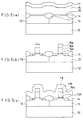
- Figs. 5 to 9 show steps of a first manufacturing method of manufacturing a semiconductor device.
- a polysilicon film is deposited on the silicon oxide film 15.
- trichrolide phosphate (POCl 3 ) gas is flowed within a diffusion furnace.
- a first HTO film 17 is deposited on the N-type polysilicon film 16.
- etch back is performed on the second HTO film 18, thereby forming a gate electrode side-wall 18A as shown in Fig. 6(a).
- Arsenic and boron are then ion-implanted into the semiconductor substrate 12 to form a source/drain region 19.
- a third HTO film 20 after depositing a third HTO film 20, a polysilicon film 21 into which an impurity is implanted, a tungsten silicide film 22 and a fourth HTO film 23 in this order, photolithography and dry etching are performed on the polysilicon film 21, the tungsten silicide film 22 and the fourth HTO film 23, thereby forming a polycide wire 24 which is formed by the polysilicon film 21 and the tungsten silicide film 22 and an above-the-wire insulating film 23A which is formed by the fourth HTO film 23 as shown in Fig 7(a).
- the third HTO film 20 and the fourth HTO film 23 are deposited by the method of forming a silicon oxide film according to the first or the second preferred embodiment.
- etch back is performed on the fifth HTO film 25, whereby a wire side-wall 25A is formed as shown in Fig. 8(a).
- a contact hole is made in the first inter-layer insulating film 26.
- a contact by depositing titanium 27, titanium nitride 28 and tungsten 29 in this order in the contact hole, a first aluminum wire 30 is formed.
- a contact hole is made in the second inter-layer insulating film 31.
- a phosphate glass (PSG) film 33 and a silicon nitride film 34 are deposited in this order by a plasma CVD method, whereby a passivation film is formed.
- An opening portion 35 for an electrode pad is thereafter formed in the phosphate glass film 33 and the silicon nitride film 34.
- the impurity within the N - layer and the source/drain region 19 which are formed in the semiconductor substrate 12 is diffused in a planar direction of the substrate. This reduces the effective gate length (L eff ).
- L eff effective gate length
- silicide films such as a titanium silicide film, may be deposited as protection films.
- Fig. 10 shows a degree of a decrease ( ⁇ L eff ) in the effective channel length in cases where an HTO film is deposited under the conditions which were used in the concrete and the comparison examples.
- ⁇ L eff (a decrease in L eff which is created during the manufacturing processes where an HTO film is deposited under the conditions used in the comparison example)
- a decrease in L eff which is created during the manufacturing processes where an HTO film is deposited under the conditions used in the concrete example a decrease in L eff which is created during the manufacturing processes where an HTO film is deposited under the conditions used in the concrete example
- the degree of the decrease in the effective channel length: ⁇ L eff is 0.05 to 0.10 ⁇ m in the case of an N-channel transistor, but 0.06 to 0.12 ⁇ m in the case of a P-channel transistor.
- L eff it is possible to suppress a decrease in the effective channel length: L eff by maximum about 0.1 ⁇ m in the case of an N-channel transistor, by maximum about 0.12 ⁇ m in the case of a P-channel transistor.
- the effect of preventing a decrease in the effective channel length: L eff is large particularly in a transistor with a rule of 0.5 ⁇ m or smaller. Since excessive thermal diffusion of an impurity is suppressed by depositing the HTO film under the conditions used in the first and the second preferred embodiments, it is possible to improve a transistor performance and to prevent deterioration in an element separating characteristic.
- Figs. 11 to 13 show steps of a second manufacturing method of manufacturing a semiconductor device which is formed by a flash EEPROM (Electrical Erasable Programmable Read Only Memory).
- flash EEPROM Electrical Erasable Programmable Read Only Memory
- a polysilicon film is deposited on the silicon oxide film 45.
- trichrolide phosphate (POCl 3 ) gas is flowed within a diffusion furnace to introduce phosphorus into the polysilicon film, whereby a first N-type polysilicon film 46 is formed.
- a second N-type polysilicon film 48 which is doped with phosphorus is deposited on the first HTO film 47.
- photolithography and dry etching are performed on the first HTO film 47 and the second N-type polysilicon film 48, to thereby form an under-the-gate insulating film 45A, a floating gate electrode 46A, an inter-gate insulating film 47A and a control gate electrode 48A.
- phosphorus is ion-implanted into the semiconductor substrate 42 to form an N - region.
- etch back is performed on the second HTO film to form a gate electrode side-wall 49.
- Arsenic and boron are then ion-implanted into the semiconductor substrate 42 to form a source/drain region 50.
- a contact hole is made in the first inter-layer insulating film 51.
- a contact by depositing titanium 52, titanium nitride 53 and tungsten 54 in this order in the contact hole, a first aluminum wire 55 is formed.
- a contact hole is made in the second inter-layer insulating film 56.
- a phosphate glass (PSG) film 58 and a silicon nitride film 59 are deposited in this order by a plasma CVD method, whereby a passivation film is formed.
- An opening portion 60 for an electrode pad is thereafter formed in the phosphate glass film 58 and the silicon nitride film 59.
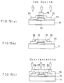
- Figs. 14 and 15 show steps of a third manufacturing method of manufacturing a semiconductor device which is formed by a TFT (Thin Film Transistor).
- TFT Thin Film Transistor
- a gate electrode 72 which is formed by polysilicon which is doped with high fusing point metal or an N-type impurity is formed on an ITO substrate 71.
- an HTO film 73 is deposited by the method of forming a silicon oxide film according to the first or the second preferred embodiment. Following this, after depositing an amorphous silicon film on the HTO film 73, a polysilicon film 74 having a particle diameter of a few ⁇ m or larger is formed on the amorphous silicon film by irradiation of an excimer laser.
- the polysilicon film 74 is patterned by dry etching, whereby a patterned polysilicon film 74A is formed.
- ions are implanted into the patterned polysilicon film 74A using the second resist pattern 76 as a mask, to thereby form a source/drain region 77.
- the metal film is patterned to form a source/drain electrode 78.
- the HTO film 73 is deposited by the methods of forming a silicon oxide film according to the first and the second preferred embodiments, it is possible to suppress a variation in the film thickness of the HTO film 73, and therefore, to stabilize a gate current and reduce thermal damage to the ITO substrate 71. This makes it possible to manufacture a TFT of an excellent quality at a good yield.
Landscapes
- Chemical & Material Sciences (AREA)
- Inorganic Chemistry (AREA)
- General Chemical & Material Sciences (AREA)
- Chemical Kinetics & Catalysis (AREA)
- Engineering & Computer Science (AREA)
- Materials Engineering (AREA)
- Mechanical Engineering (AREA)
- Metallurgy (AREA)
- Organic Chemistry (AREA)
- Formation Of Insulating Films (AREA)
- Semiconductor Memories (AREA)
- Chemical Vapour Deposition (AREA)
Applications Claiming Priority (2)
| Application Number | Priority Date | Filing Date | Title |
|---|---|---|---|
| JP86843/95 | 1995-04-12 | ||
| JP8684395 | 1995-04-12 |
Publications (2)
| Publication Number | Publication Date |
|---|---|
| EP0738003A2 true EP0738003A2 (fr) | 1996-10-16 |
| EP0738003A3 EP0738003A3 (fr) | 1997-06-11 |
Family
ID=13898102
Family Applications (1)
| Application Number | Title | Priority Date | Filing Date |
|---|---|---|---|
| EP96105727A Withdrawn EP0738003A3 (fr) | 1995-04-12 | 1996-04-11 | Méthode pour la formation d'une couche en oxyde de silicium pour des dispositifs semi-conducteurs par dépÔt chimique en phase vapeur à basse pression (LPCVD) |
Country Status (2)
| Country | Link |
|---|---|
| EP (1) | EP0738003A3 (fr) |
| KR (1) | KR960039197A (fr) |
Cited By (7)
| Publication number | Priority date | Publication date | Assignee | Title |
|---|---|---|---|---|
| WO1999015711A1 (fr) * | 1997-09-23 | 1999-04-01 | The University Of Tennesee Research Corporation | Lamine comportant une couche barriere d'oxyde de silicium |
| GB2343197A (en) * | 1998-10-29 | 2000-05-03 | Lg Philips Lcd Co Ltd | Forming silicon oxide layer by use of two frequency excitation plasma CVD |
| EP1132959A1 (fr) | 2000-03-03 | 2001-09-12 | STMicroelectronics S.r.l. | Procédé de fabrication de connection à basse résistivité dans une mémoire non-volatile |
| US6630378B1 (en) * | 1996-03-27 | 2003-10-07 | Nec Electronics Corporation | Method of fabricating a dynamic random access memory device having stacked capacitor memory cell arrays |
| CN104099581A (zh) * | 2014-07-23 | 2014-10-15 | 国家纳米科学中心 | 一种氧化硅膜材料及其制备方法 |
| CN103787325B (zh) * | 2014-02-21 | 2016-08-24 | 中山大学 | 一种石墨烯器件的制备方法 |
| CN115467021A (zh) * | 2022-09-22 | 2022-12-13 | 广州粤芯半导体技术有限公司 | 低缺陷掺杂多晶硅及其制备方法 |
Family Cites Families (7)
| Publication number | Priority date | Publication date | Assignee | Title |
|---|---|---|---|---|
| US4419809A (en) * | 1981-12-30 | 1983-12-13 | International Business Machines Corporation | Fabrication process of sub-micrometer channel length MOSFETs |
| US4458407A (en) * | 1983-04-01 | 1984-07-10 | International Business Machines Corporation | Process for fabricating semi-conductive oxide between two poly silicon gate electrodes |
| JPH02294040A (ja) * | 1989-05-09 | 1990-12-05 | Hitachi Ltd | 半導体装置およびその製造方法 |
| US5250468A (en) * | 1990-02-05 | 1993-10-05 | Mitsubishi Denki Kabushiki Kaisha | Method of manufacturing semiconductor device including interlaying insulating film |
| US5366917A (en) * | 1990-03-20 | 1994-11-22 | Nec Corporation | Method for fabricating polycrystalline silicon having micro roughness on the surface |
| WO1991017839A1 (fr) * | 1990-05-18 | 1991-11-28 | Bp Chemicals (Hitco) Inc. | Materiaux destines aux procedes chimiques de depot en phase gazeuse |
| US5306657A (en) * | 1993-03-22 | 1994-04-26 | United Microelectronics Corporation | Process for forming an FET read only memory device |
-
1996
- 1996-03-20 KR KR1019960007624A patent/KR960039197A/ko not_active Ceased
- 1996-04-11 EP EP96105727A patent/EP0738003A3/fr not_active Withdrawn
Cited By (15)
| Publication number | Priority date | Publication date | Assignee | Title |
|---|---|---|---|---|
| US6630378B1 (en) * | 1996-03-27 | 2003-10-07 | Nec Electronics Corporation | Method of fabricating a dynamic random access memory device having stacked capacitor memory cell arrays |
| WO1999015711A1 (fr) * | 1997-09-23 | 1999-04-01 | The University Of Tennesee Research Corporation | Lamine comportant une couche barriere d'oxyde de silicium |
| DE19952316B4 (de) * | 1998-10-29 | 2004-05-06 | Lg. Philips Lcd Co., Ltd. | Verfahren zum Herstellen einer Gateisolierung und einer Trennisolierung in einem Dünnfilmtransistor |
| US6337292B1 (en) | 1998-10-29 | 2002-01-08 | Lg. Philips Lcd Co., Ltd. | Method of forming silicon oxide layer and method of manufacturing thin film transistor thereby |
| US6627545B2 (en) | 1998-10-29 | 2003-09-30 | Lg.Philips Lcd Co., Ltd | Method of forming silicon oxide layer and method of manufacturing thin film transistor thereby |
| GB2343197B (en) * | 1998-10-29 | 2001-01-10 | Lg Philips Lcd Co Ltd | Method of forming silicon oxide layer and method of manufacturing thin film transistor thereby |
| US6716752B2 (en) | 1998-10-29 | 2004-04-06 | Lg.Philips Lcd Co., Ltd. | Method of forming silicon oxide layer and method of manufacturing thin film transistor thereby |
| GB2343197A (en) * | 1998-10-29 | 2000-05-03 | Lg Philips Lcd Co Ltd | Forming silicon oxide layer by use of two frequency excitation plasma CVD |
| US7378304B2 (en) | 1998-10-29 | 2008-05-27 | Lg.Philips Lcd Co., Ltd. | Method of forming silicon oxide layer and method of manufacturing thin film transistor thereby |
| EP1132959A1 (fr) | 2000-03-03 | 2001-09-12 | STMicroelectronics S.r.l. | Procédé de fabrication de connection à basse résistivité dans une mémoire non-volatile |
| US6686241B2 (en) | 2000-03-03 | 2004-02-03 | Stmicroelectronics S.R.L. | Method of forming low-resistivity connections in non-volatile memories |
| CN103787325B (zh) * | 2014-02-21 | 2016-08-24 | 中山大学 | 一种石墨烯器件的制备方法 |
| CN104099581A (zh) * | 2014-07-23 | 2014-10-15 | 国家纳米科学中心 | 一种氧化硅膜材料及其制备方法 |
| CN115467021A (zh) * | 2022-09-22 | 2022-12-13 | 广州粤芯半导体技术有限公司 | 低缺陷掺杂多晶硅及其制备方法 |
| CN115467021B (zh) * | 2022-09-22 | 2023-12-12 | 粤芯半导体技术股份有限公司 | 低缺陷掺杂多晶硅及其制备方法 |
Also Published As
| Publication number | Publication date |
|---|---|
| KR960039197A (ko) | 1996-11-21 |
| EP0738003A3 (fr) | 1997-06-11 |
Similar Documents
| Publication | Publication Date | Title |
|---|---|---|
| US5578524A (en) | Fabrication process of a semiconductor device with a wiring structure | |
| KR970009867B1 (ko) | 반도체 소자의 텅스텐 실리사이드 형성방법 | |
| US20070066077A1 (en) | Method for manufacturing semiconductor device | |
| KR100253875B1 (ko) | 반도체장치 및 그 제조방법(a semiconductor device and a method for manufacturing thereof) | |
| JP2607503B2 (ja) | 二重誘電体mosゲート絶縁装置とその形成方法 | |
| KR100456315B1 (ko) | 반도체소자의 게이트전극 형성방법 | |
| EP0738003A2 (fr) | Méthode pour la formation d'une couche en oxyde de silicium pour des dispositifs semi-conducteurs par dépÔt chimique en phase vapeur à basse pression (LPCVD) | |
| KR100562541B1 (ko) | Cvd 실리콘 옥시나이트라이드층에 의해 후처리되는sion/teos 층간 유전체 형성 방법 | |
| US6777354B2 (en) | Semiconductor device and method of manufacturing the same | |
| US6274429B1 (en) | Use of Si-rich oxide film as a chemical potential barrier for controlled oxidation | |
| US7049236B2 (en) | Method of manufacturing a semiconductor device | |
| US6777764B2 (en) | ONO interpoly dielectric for flash memory cells and method for fabricating the same using a single wafer low temperature deposition process | |
| KR20000001625A (ko) | 2중층 스페이서를 갖는 모스 트랜지스터 형성방법 | |
| KR100537276B1 (ko) | 반도체 소자의 제조 방법 | |
| US7592240B2 (en) | Method for forming a gate structure through an amorphous silicon layer and applications thereof | |
| KR20030050652A (ko) | 텅스텐막의 형성 방법 | |
| JPH08339995A (ja) | シリコン酸化膜の形成方法及び半導体装置の製造方法 | |
| KR100573482B1 (ko) | 반도체 소자의 폴리 실리콘막 형성방법 | |
| KR0135223B1 (ko) | 반도체소자의 게이트 전극 형성방법 | |
| KR0119965B1 (ko) | 반도체 소자의 산화막 형성방법 | |
| KR100472855B1 (ko) | 반도체소자의다결정실리콘박막제조방법 | |
| JP3437111B2 (ja) | 半導体装置の製造方法 | |
| JPH09219452A (ja) | ボロンリンガラス膜の溶融平坦化方法 | |
| KR100456260B1 (ko) | 반도체소자의게이트전극형성방법 | |
| KR100321720B1 (ko) | 텅스텐폴리사이드구조를가진모스트랜지스터의게이트전극형성방법 |
Legal Events
| Date | Code | Title | Description |
|---|---|---|---|
| PUAI | Public reference made under article 153(3) epc to a published international application that has entered the european phase |
Free format text: ORIGINAL CODE: 0009012 |
|
| AK | Designated contracting states |
Kind code of ref document: A2 Designated state(s): DE GB |
|
| PUAL | Search report despatched |
Free format text: ORIGINAL CODE: 0009013 |
|
| AK | Designated contracting states |
Kind code of ref document: A3 Designated state(s): DE GB |
|
| 17P | Request for examination filed |
Effective date: 19970626 |
|
| STAA | Information on the status of an ep patent application or granted ep patent |
Free format text: STATUS: THE APPLICATION IS DEEMED TO BE WITHDRAWN |
|
| 18D | Application deemed to be withdrawn |
Effective date: 19991103 |