EP0738054A2 - Circuit PLL pour récepteur de radiodiffusion numérique - Google Patents
Circuit PLL pour récepteur de radiodiffusion numérique Download PDFInfo
- Publication number
- EP0738054A2 EP0738054A2 EP96302626A EP96302626A EP0738054A2 EP 0738054 A2 EP0738054 A2 EP 0738054A2 EP 96302626 A EP96302626 A EP 96302626A EP 96302626 A EP96302626 A EP 96302626A EP 0738054 A2 EP0738054 A2 EP 0738054A2
- Authority
- EP
- European Patent Office
- Prior art keywords
- signal
- counter
- time
- phase
- output
- Prior art date
- Legal status (The legal status is an assumption and is not a legal conclusion. Google has not performed a legal analysis and makes no representation as to the accuracy of the status listed.)
- Withdrawn
Links
Images









Classifications
-
- H—ELECTRICITY
- H04—ELECTRIC COMMUNICATION TECHNIQUE
- H04N—PICTORIAL COMMUNICATION, e.g. TELEVISION
- H04N7/00—Television systems
- H04N7/24—Systems for the transmission of television signals using pulse code modulation
- H04N7/52—Systems for transmission of a pulse code modulated video signal with one or more other pulse code modulated signals, e.g. an audio signal or a synchronizing signal
- H04N7/54—Systems for transmission of a pulse code modulated video signal with one or more other pulse code modulated signals, e.g. an audio signal or a synchronizing signal the signals being synchronous
- H04N7/56—Synchronising systems therefor
-
- H—ELECTRICITY
- H03—ELECTRONIC CIRCUITRY
- H03L—AUTOMATIC CONTROL, STARTING, SYNCHRONISATION OR STABILISATION OF GENERATORS OF ELECTRONIC OSCILLATIONS OR PULSES
- H03L7/00—Automatic control of frequency or phase; Synchronisation
- H03L7/06—Automatic control of frequency or phase; Synchronisation using a reference signal applied to a frequency- or phase-locked loop
- H03L7/08—Details of the phase-locked loop
- H03L7/0807—Details of the phase-locked loop concerning mainly a recovery circuit for the reference signal
-
- H—ELECTRICITY
- H03—ELECTRONIC CIRCUITRY
- H03L—AUTOMATIC CONTROL, STARTING, SYNCHRONISATION OR STABILISATION OF GENERATORS OF ELECTRONIC OSCILLATIONS OR PULSES
- H03L7/00—Automatic control of frequency or phase; Synchronisation
- H03L7/06—Automatic control of frequency or phase; Synchronisation using a reference signal applied to a frequency- or phase-locked loop
- H03L7/08—Details of the phase-locked loop
- H03L7/085—Details of the phase-locked loop concerning mainly the frequency- or phase-detection arrangement including the filtering or amplification of its output signal
- H03L7/093—Details of the phase-locked loop concerning mainly the frequency- or phase-detection arrangement including the filtering or amplification of its output signal using special filtering or amplification characteristics in the loop
-
- H—ELECTRICITY
- H03—ELECTRONIC CIRCUITRY
- H03L—AUTOMATIC CONTROL, STARTING, SYNCHRONISATION OR STABILISATION OF GENERATORS OF ELECTRONIC OSCILLATIONS OR PULSES
- H03L7/00—Automatic control of frequency or phase; Synchronisation
- H03L7/06—Automatic control of frequency or phase; Synchronisation using a reference signal applied to a frequency- or phase-locked loop
- H03L7/16—Indirect frequency synthesis, i.e. generating a desired one of a number of predetermined frequencies using a frequency- or phase-locked loop
- H03L7/18—Indirect frequency synthesis, i.e. generating a desired one of a number of predetermined frequencies using a frequency- or phase-locked loop using a frequency divider or counter in the loop
-
- H—ELECTRICITY
- H04—ELECTRIC COMMUNICATION TECHNIQUE
- H04L—TRANSMISSION OF DIGITAL INFORMATION, e.g. TELEGRAPHIC COMMUNICATION
- H04L7/00—Arrangements for synchronising receiver with transmitter
- H04L7/02—Speed or phase control by the received code signals, the signals containing no special synchronisation information
- H04L7/033—Speed or phase control by the received code signals, the signals containing no special synchronisation information using the transitions of the received signal to control the phase of the synchronising-signal-generating means, e.g. using a phase-locked loop
Definitions
- the present invention generally relates to a PLL circuit and method therefor used in receivers in a digital broadcasting systems for obtaining clocks synchronized with system clocks at a transmitter in the digital broadcasting system from a system clock regenerating signal extracted from a bit stream.
- a transmission architecture for multiplexing signals such as a video signal, an audio signal, a data signal, etc. to transmit them as a bit stream has been established.
- the receiver In this transmission system, the receiver must reproduce system clocks synchronized with the transmission side and perform the signal processing. So, signals required for reproducing the system clocks are transmitted by inserting them in a bit stream at a proper interval. In the receiver these signals are extracted from the bit stream and clocks synchronizing the system clocks at the transmitter are obtained by a PLL (Phase Locked Loop) processing.
- PLL Phase Locked Loop
- the broadcasting in accordance with the ISO/IEC 13818 (hereinafter referred to as the MPEG.2) is highlighted for the digital broadcasting.
- signals such as video signals, audio signals, data signals, etc. are packetized, multiplexed and transmitted as a transport stream.
- PCRs program clock references
- This PCR is an output of a counter which runs under a control of the system clocks.
- PCR.b program clock reference base
- PCR.ex program clock reference extension
- FIGURE 19 shows a PLL circuit for a system proposed in the MPEG2 system.
- the transport stream described above is applied to a terminal 11.
- a program selecting signal showing a program which is selected by a user is applied to a terminal 12, and a power ON reset signal showing the initialization at the time- of power ON is applied to a terminal 13.
- the transport stream which has been applied to the terminal 11 is further applied to a PCR extractor 14. Further, the program selecting Signal applied to the terminal 12 is further applied to both the PCR extractor 14 and a program switching signal generator 15 and is converted to a program switching signal which generates pulses when a program is switched.
- the PCR of the program directed to select by the program selecting signal is extracted from the input transport stream, and at the same time, a PCR field detection signal showing portions of the transport stream in which the selected program PCRs have been inserted and a time base switching signal showing the completion of the time-base switching are output.
- the time base generally changes and the assignment of PCR also changes. Further, the time base switching signal changes to a signal containing pulses at timings where the time base changes.
- the PCR field detection signal output from the PCR extractor 14 is applied to a timing signal generator 16.
- This timing signal generator 16 generates various timing signals, e.g., a master timing signal, a load timing signal, etc. from the PCR field detection signal.
- the PCR extracted by the PCR extractor 14 is transmitted to a latch17 where it is latched by a master timing signal from the timing signal generator 16. This latch signal is applied to a subtractor 21.
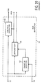
- FIGURE 20 The arrangement of the PCR extractor 14 is shown in FIGURE 20.
- a transport stream input through the terminal 11 is applied to a packet ID selecting circuit 141, a depacketizer 142 and a PCR field extractor 143. Further, a program selecting signal input through the terminal 12 is applied to the packet ID selector 141.
- a packet ID is a peculiar ID assigned by program according to respective transport streams of video, audio, data, etc.
- the packet ID selector 141 a program signal showing a program stream in which the PCR is inserted is captured from the transport stream. Then, a packet ID is extracted from the captured program signal by discriminating a transport stream in which a user-selected program PCR is inserted based on a program selecting signal. The packet ID output from this packet ID selector 141 is applied to the depacketizer 142.
- This depacketizer 142 first detects a packet having the packet ID, which is output from the packet ID selector 141, from a transport stream. Then, a header of the detected packet is analyzed to judge a location where a PCR is placed in the detected packet. Then based on the result of this analysis, the depacketizer 142 outputs a PCR field detection signal showing a location in the transport stream where the PCR is placed. Further, by analyzing the header of the detected packet, a discontinuity indicator serving as a flag related to a time base, is detected and by checking the state of this flag, whether a time base is switched is judged. If a time base has switched, a time base switching signal pulse is output.
- the PCR field detection signal which is output from this depacketizer 142 is applied to both the PCR field extractor 143 and the timing signal generator 16. Further, a time base switching signal is supplied to an AND gate of a load controller 18.
- PCR field extractor 143 an operation to extract a PCR field from a transport stream is carried out according to the PCR field detection signal.
- the PCR extracted in the PCR field extractor 143 is transmitted to the latch 17 and a counter 19 as an output of the PCR extractor 14.
- the PCR which is output from the PCR extractor 14 is loaded under a control of a load control signal output from the load controller 18 and perform the counting operation by system clocks output from a VCXO (voltage controlled oscillator) 23 and an output of this counter 19 is applied to a latch 20 and is latched therein by the master timing signal output from the timing signal generator 16.
- the count latched by the latch 20 is applied to a subtractor 21.
- a difference between a value of the PCR output from the latch 17 and the count of the counter 19 output from the latch 20 is calculated.
- a difference output from the subtractor 21 is converted to a voltage signal by a low-pass filter (LPF) and applied to the VCXO 23 as a frequency control signal. Therefore, a system clock with a frequency corresponding to the difference between the PCR and the output of the counter 19 is output from the VCXO.
- LPF low-pass filter
- the load controller 18 is comprised of the AND gate 181 and a load control signal generator 182.
- an AND logic (logical product) is operated by inputting a time base switching signal output from the PCR extractor 14, the program switching signal output from the program switching signal generator 15 and the power ON reset signal input from the terminal 13.
- the calculation result of the AND logic is applied to the load control signal generator 182.
- a load control signal is generated from the master timing signal and the load timing signal which are output from the timing signal generator 16 and the output signal of the AND gate 181. This load control signal is supplied to the counter 19.
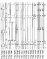
- FIGURE 21 is a timing chart showing output timings of major parts of the PLL circuit shown in FIGURE 19.
- the operation of the PLL circuit with the arrangement as described above will be explained referring to FIGURE 21.
- FIGURE 21(a) shows a transport stream which is input through the terminal 11. This transport stream has PCRs of a user-selected program inserted at the locations P1, P2, P3 and P4.
- FIGURE 21(b) shows the PCR field detection signal which is output from the PCR extractor 14.
- This PCR field detection signal in synchronous with the transport stream shows portions of the transport stream in which the PCRs are inserted by outputting it at a low level for the duration in which the PCR is inserted. So, the PCR field detection signal shown in FIGURE 2(b) is at the low level in the durations of P1, P2, P3 and P4 of the transport stream shown in FIGURE 21(b).
- FIGURE 21(c) shows the output of the PCR extractor 14. That is, in the PCR extractor 14, the P1, P2, P3 and P4 which are the PCRs of a user-selected program inserted in the transport stream shown in FIGURE 21(a) are extracted as shown in FIGURE 21(c).
- FIGURE 21(d) shows the master timing signal which is output from the timing signal generator 16. This master timing signal is generated in the timing signal generator 16 based on the PCR field detection signal shown in FIGURE 21(b).
- FIGURE 21(e) shows the output of the latch 17.
- the PCR which is the output of the PCR extractor 14 shown in FIGURE 21(c) is latched in the latch 17 by the master timing signal shown in FIGURE 21(d) and its output changes as shown in FIGURE 21(e) and is applied to the subtractor 21.
- FIGURE 21(f) shows the output of the AND gate 181. This signal shows whether a program has been switched or the power source has been turned ON or a time base has been switched at the time (A) when a low level pulse is generated and is supplied to the load control signal generator 182.
- FIGURE 21(g) shows the load timing signal which is output from the timing signal generator 16. This load timing signal is applied to the load control signal generator 182 together with the output signal of the AND gate 181 shown in FIGURE 21(f) and the master timing signal shown in FIGURE 21(d).
- FIGURE 21(h) shows the load control signal generated in the load control signal generator 182. That is, the load control signal generator 182 outputs the load control signal which changes to a low level pulse in the duration TO until the time (C) when a subtraction of the first PCR and the count is performed immediately after a program switching, a time base switching or the power ON.
- FIGURE 21(i) shows the output of the counter 19. That is, the counter 19 loads the PCR which is output from the PCR extractor 14 when the load control signal is at the low level.
- P1 which is the value of the PCR output from the PCR extractor 14, is loaded on the counter 19 at the time (B) immediately after the load control signal generates a low level pulse and is applied to the latch 20 as the output of the counter 19 as shown in FIGURE 21(i).
- FIGURE 21(j) shows the output signal of the latch 20. That is, the output of the counter 19 shown in FIGURE (i) is applied to the latch 20 and latched by the master timing signal (see FIGURE 21(d)) and an output shown in FIGURE 21(i) is obtained and applied to the subtractor 21.
- FIGURE 21(k) shows the output of the subtractor 21. That is, in the subtractor 21 a difference between the PCR output from the latch 17 shown in FIGURE 21(e) and the count of the counter 19 output from the latch 20 shown in FIGURE 21(j) is calculated and then applied to the low pass filter 22.
- the output of the subtractor 21 in the period T2 is a positive value, the output of the subtractor 21 is so controlled that the frequency of the system clock output from the VCXO is increased. Further, in the period T3, a difference ⁇ K3 between the PCR P3 and the output S3 of the counter 19 is so controlled that it becomes smaller than the ⁇ K2. As such operations are repeated, the output of the subtractor 21 become 0. That is, when the output of the subtractor 21 becomes 0, the transmitted and received system clock frequencies and phases are synchronized each other.
- a duration for obtaining a difference between the PCR and the count is not constant. So, a factor of the PCR insertion interval is involved in a difference which controls the VCXO and a difference between the PCR and the output of the counter does not depend on only a deviation between frequencies and phases of transmitted and received system clocks.
- a conventional PLL circuit has such a problem in that the system clock frequency is not precisely controlled for the VCXO.
- PCRs are once loaded on a counter immediately after a program switching, a time base switching or power ON and after matching a PCR with a counter output, the frequency and the phase of the system clock are locked at the receiver. Therefore, it has such a problem in that a certain length of time is required until the frequency and the phase of the system clock are locked.
- an object of the present invention to provide a PLL circuit and method capable of reducing the time required to lock the frequency and the phase of the system clock at the receiver and accurately controlling the system clock frequency.
- a PLL circuit or method for use in a digital broadcasting receiver includes; means for or step of receiving a bit stream transmitted from a broadcast station, the bit stream containing a time-signal and a phase-signal, an oscillator for or step of generating system clocks, a counter for or step ofoperating in response to the system clocks from the oscillator, means for applying the bit stream from the receiving means to the oscillator, means for or step of controlling the counter so that the counter output matches with the time-signal and the phase-signal, based on differences between both of the time-signal and the phase-signal through the applying means and the counter output, and load control means for or step of successively loading twice the time-signal and the phase-signal on the counter in the transmission order of the signals, in the course for locking the frequency and the phase of the system clock provided from the oscillator.
- a second aspect of the PLL circuit or method for use in a digital broadcasting receiver includes; means for or step of receiving a bit stream transmitted from a broadcast station, the bit stream containing a time-signal and a phase-signal, an oscillator for or step of generating system clocks, a first counter for or step of operating in response to the system clocks from the oscillator, means for or step of applying the bit stream from the receiving means to the oscillator, means for or step of controlling the first counter so that the counter output matches with the time-signal and the phase-signal, based on differences between both of the time-signal and the phase-signal through the applying means and the counter output, and means for or step of compensating a difference between the time-signal and the phase-signal in the bit stream and the output of the first counter according to insertion intervals of the time-signal and the phase-signal in the bit stream.
- the PCRs (the time-signal and the phase-signal inserted in a bit stream) are once loaded on a counter, a difference between a PCR and a counter output is calculated. Then, a difference between a PCR and a counter output is calculated at the timing when the PCR has been transmitted, and then the PCR is loaded on the counter.
- a difference between the PCR and the counter output is normalized by compensating it in accordance with the insertion intervals of the PCRs.
- This normalization denotes that a difference between a PCR and a counter output does not depend on the PCR insertion interval.
- FIGURES 1 through 18 are views illustrating preferred embodiments according to the present invention.
- FIGURE 1 shows a first embodiment of the PLL circuit according to the present invention.
- the same reference numerals are assigned to the same parts as in FIGURE 19 and only elements differing from those shown in FIGURE 19 will be described here.
- a time required for locking the frequency and the phase of the system clocks at the receiver which has been a problem in a conventional example, has been improved by loading the PCRs on the counter continuously twice.
- This embodiment features the arrangement of the load controller 18. That is, this load controller 18 is provided with a load control signal generating counter 186, a first load control signal generator 183, a second load control signal generator 184 and an AND gate 185 in addition to the AND gate 181 which has been described above.
- a master timing signal is generated from the PCR field detection signal and also, a first and a second load timing signals are generated and applied to the load control signal generators 183 and 184, respectively.
- the AND gate 18 is input a time base switching signal which is output from the PCR extractor 14 and a power ON reset signal whiah is output from the terminal 13 and thus performs an AND operation. The result of this operation is applied to a load control signal generating counter 186.
- the load control signal generating counter 186 operates using the master timing signal output from the timing signal generator 16 as a clock input and the output signal of the AND gate 181 as a reset signal.
- the output of the load control signal generating counter 186 is applied to the first and the second load control signal generators 183 and 184, respectively.
- the first load control signal generator 183 generates a first load control signal from the output of the load control signal generating counter 186 and the first load timing signal output from the timing signal generator 16. Further, the second load control signal generator 184 generates a second load control signal from the output of the load control signal generating counter 186 and the second load timing signal output from the timing signal generator 16.
- the first and the second load control signals are applied to the AND gate 185, where an AND logic of both signals is operated and the result is applied to the counter 19 as a load control signal.
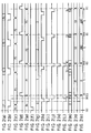
- FIGURE 2 shows output timings of major parts and FIGURE 2(a) shows a transport stream which is input through the terminal 11.
- the PCRs of a user-selected program have been inserted at the locations P1, P2, P3 and P4.
- This transport stream is applied to the PCR extractor 14, wherein the PCR field detection signal shown in FIGURE 2(b) is generated.
- This PCR field detection signal in synchronous with the transport stream shows locations where the PCRs are inserted and at the low level in the duration when the PCRs are inserted, that is, in the durations of P1, P2, P3 and P4 of the transport stream shown in FIGURE 2(a).
- This PCR field detection signal is applied to the timing signal generator 16.
- P1, P2, P3 and P4 which are the PCRs of a user-selected program inserted in the transport stream shown in FIGURE 2(a) have been extracted as shown in FIGURE 2(c).
- the extracted PCRs are applied to the latch 17 and the counter 19.
- the master timing signal shown in FIGURE 2(d) is generated based on the PCR field detection signal shown in FIGURE 2(b). Further, in the latching circuit 17, the PCRs extracted by the PCR extractor 14 shown in FIGURE 2(c) are latched by the master timing signal shown in FIGURE 2(d) as shown in FIGURE 2(e). The latched outputs are applied to the subtractor 21.
- this pulse shows the program switching, the power source ON or a time base switching and is applied to the load control signal generating counter 186.
- the master timing signal output from the timing signal generator 16 is applied to the load control signal generating counter 186 as the master timing signal and the output signal of the AND gate 181 is input as the reset signal. That is, this counter 186 is reset when the output signal of the AND gate 181 drops to the low level. Thereafter, if the reset is canceled, the counter 186 sequentially counts up in every leading edge of the master timing signal which has been input as a clock input. So, the outputs of the load control signal generating counter 186 will be as shown in FIGURE 2(g). The outputs of this counter 186 are applied to the first and the second load control signal generators 183 and 184.
- the first load timing signal shown in FIGURE 2(h) and the output signal of the load control signal generating counter 186 shown in FIGURE 2(g) are applied to the first load control signal generator 183.
- the first load timing signal shown in FIGURE 2(h) is generated in the timing signal generator 16 based on the PCR field detection signal shown in FIGURE 2(b) and its load timing is such that the PCRs are loaded on the counter 19 in the duration at the low level.
- the first load control signal generator 183 outputs a signal shown in FIGURE 2(i). Only when the output signal of the load control signal generating counter 186 is 0, this signal passes through the first load timing signal and is at the high level in the period when the output of the load control signal generating counter 186 has a different value.
- the second load control signal generator 184 the second load timing signal shown in FIGURE 2(j) and the output signal of the load control signal generating counter 186 shown in FIGURE 2(g) are input.
- the second load timing signal shown in FIGURE 2(j) is generated in the timing signal generator 16 based on the PCR field detection signal and its load timing is such that the PCRs are loaded on the counter 19 in the duration at the low level state.
- the second load control signal generator 184 outputs the signal shown in FIGURE 2(k). Only when the output signal of the load control signal generating counter 186 is 1, this signal passes through the second load timing signal and stays at the high level in the duration when the output of the load control signal generating counter has a different value.
- the first load control signal shown in FIGURE 2(i) and the second load control signal shown in FIGURE 2(k) are applied to the AND gate 185 and the load control signal shown in FIGURE 2(1) is obtained from the AND operation.
- This load control signal controls the loading operation to the counter 19 and the loading operation to the counter 19 is allowed when this load control signal is at the low level.
- the load control signal is at the low level immediately before the times (B) and (D).
- the output of the PCR extractor 14 shown in FIGURE 2(c) during this period has the value P1 at the time (B) and P2 at the time (D) and these values are loaded on the counter 19.
- P1 and P2 values loaded on the counter 19 are output immediately after the times (B) and (D) as the outputs of the counter 19 as shown in FIGURE 2(m). That is, after outputting the PCR P1 loaded immediately after the time (B), the counter 19 makes the counting in order until S2 is output immediately before the time (D) and outputs the PCR P2 loaded again immediately after the time (D). Thereafter the count-up operation continues in the order.
- the output of the counter 19 shown in FIGURE 2(m) is latched by the master timing signal (see FIGURE 2(d)) in the latch 20, turned to a signal shown in FIGURE 2(n), and applied to the subtractor 21.
- the output 0 of the subtractor 21 passes through the low-pass filter 22 to control the VCXO 23.
- the VCXO 23 outputs a system clock having frequency f1 corresponding to a value obtained by passing the output 0 of the subtractor 21 through the low-pass filter 22.
- the ⁇ K2 is a value resulting from a difference between the transmitted and received system clock frequencies
- the VCXO 23 is controlled by this K2 after passing through the low-pass filter 22, it is possible to make the system clock frequency obtained from the VCXO 23 to a value close to the system clock frequency fM at the transmitter.
- FIGURE 3 shows a second embodiment of the PLL circuit according to the present invention.
- the same reference numerals are assigned to the same elements as in FIGURE 19 and elements differing from those shown in FIGURE 19 will be explained here.
- a conventional PLL circuit has been improved by adding a compensator 31 so that the difference between the PCR and the count of the counter 19 is normalized and the VCXO 23 is accurately controlled.
- a difference between the PCR output from the subtractor 21 and the count of the counter 19 is applied to the compensator 31.
- This compensator 31 normalizes the difference output from the subtractor 21 by compensating it to reflect the PCR insertion interval according to a compensation timing signal output from the timing signal generator 16.
- timing signal generator 16 generates a compensation timing signal by producing pulses at the locations of a transport stream, wherein the PCRs are inserted.
- FIGURE 4 The definite arrangement of the compensator 31 is shown in FIGURE 4.
- 311 is a terminal to which a difference output from the subtractor 21 is input
- 312 is a terminal to which the compensation timing signal output from the timing signal generator 16 is input.
- the compensator 31 is comprised of a multiplier 313, a coefficient generator 314 and a counter 315.
- FIGURE 5(a) shows the output of the latch 17.
- FIGURE 5(b) shows the compensation timing signal.
- FIGURE 5(c) shows the output of the latch 20.
- FIGURE 5(d) shows the output of the subtractor 21.
- FIGURE 5(e) shows the output of the compensator 31.
- the operation of the compensator 31 shown in FIGURE 4 is described referring to FIGURES 5(a) through 5(e) in the following.
- the compensation timing signal which is applied to the terminal 312 from the timing signal generator 16 changes to the reset signal of the counter 315.
- This counter 315 counts the period until it is reset according to a clock ⁇ and the output result is applied to the coefficient generator 314.
- the clock &5 is a clock which is used when transmitting a transport stream. By continuing the count up of a period until the counter 315 is reset, it is possible to measure the insertion intervals of the PCRs.
- the output of the subtractor 21 depends on the PCR insertion interval.
- the factor of the PCR insertion interval is canceled and it takes a value which does not depend on the PCR insertion interval.
- FIGURE 6 shows the arrangement of the PLL circuit involved in the third embodiment according to the present invention.
- the same reference numerals are assigned to the same elements as those in FIGURE 19 and elements differing from those shown in FIGURE 19 will be described here.
- a conventional PLL circuit has been improved by adding a compensator 32 so as to normalize a difference between the PCR and the count and accurately control the VCXO 23, and the arrangement of the compensator 31 used in the second embodiment has been changed but the basic operation is the same as that of the second embodiment.
- the PCR extracted from the PCR extractor 14 is latched by the master timing signal in the latch 17 and applied to the subtractor 21 and the compensator 32.
- the count output from the latch 20 is subtracted from the PCR output from the latch 17.
- the difference between the PCR and the count output from the subtractor 21 is applied to the compensator 32.
- the compensator 32 normalizes the difference by compensating it to reflect the PCR insertion interval.
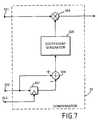
- the compensator 32 is comprised of a multiplier 324, a coefficient generator 325, a subtractor 326, and a latch 327 as shown in FIGURE 7.
- FIGURE 8 shows a timing chart explaining the operation to normalize the output of the subtractor 21, which is the difference between the PCR and the count.
- the operation of the compensator 32 shown in FIGURE 7 will be explained using the timing chart shown in FIGURE 8.
- FIGURE 8(a) the PCR which is the output of the latch 17 is latched according to the master timing signal (see FIGURE 8(b)) input from the terminal 323 and applied to the subtractor 326.
- the output signal of the latch 327 is shown in FIGURE 8(e).
- the output signal of the subtractor 326 is a difference between PCRs which are transmitted adjacently and a value showing the insertion interval of PCRs.
- the value P1 of the PCR which is output from the latch 17, shows the PCR at the time (A).
- the values P2 and P3 show the PCRs at the times (B) and (C), respectively.
- durations of the periods T1, T2 and T3 are t1, t2 and t3
- the output signal P2 of the subtractor 326 will be given by the following equation:
- the output of the subtractor 326 is a signal depending on the PCR insertion interval.
- the reciprocal of this output of the subtractor 326, which is depending on the PCR insertion interval is calculated in the coefficient generator 325 and multiplied to the output signal of the subtractor 21 (see FIGURE 8(d)), which is a difference between a PCR input through the terminal 321 and a count of the counter 19 (the output of the latch 20 (see FIGURE 8(c)) in the multiplier 324.
- a PCR immediately before the time (B) has the value P2 while the output of the counter 19 has the value S2.
- the difference between the P2 and the 52 takes a value of ⁇ K2.
- the duration t1 of the period T1 gives a factor for causing the difference ⁇ K2, in addition to a factor causing The difference in frequencies in the transmitted and received system clocks.
- the output of the subtractor 21 which is a difference between the PCR and the output of the counter 19 in the compensator 32.
- the normalized difference output from the compensator 32 is not governed by the PCR inoertion interval, it is possible to pass through the low-pass filter 22 and accurately control the VCXO 23.
- FIGURE 9 shows the arrangement of the PLL circuit involved in the fourth embodiment according to the present invention.
- the same reference numerals are assigned to the same elements as those in FIGURES 1 and 3, and different elements will be explained here.
- This embodiment is a combination of the first and the second embodiments. That is, a first and a second load control signal generators 183, 184, an AND gate 185 and a load control signal generating counter 186 have been added to the load controller 18 as means for loading PCRs continuously twice. Further, the compensator 31 has been inserted between the subtractor 21 and the LPF 22 as a means for compensating and normalizing the difference between the PCR and the counter output.
- first and second load timing signals for the first and the second load control signal generators 183, 184 and a compensation timing signal for the compensator 31 are generated in the timing signal generator 16.
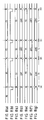
- FIGURE 10 shows the output timings of principal parts, while FIGURE 10(a) shows a transport stream which is input through the terminal 11. User-selected program PCRs have been inserted in this transport stream at the locations P1, P2, P3 and P4.
- This transport stream is applied to the PCR extractor 14, wherein the PCR field detection signal shown in FIGURE 10(b) is generated.
- This PCR field detection signal in synchronous with the transport stream shows portions of the transport stream in which PCRs have been inserted. This signal is at the low level in the periods when PCRs have been inserted, that is, the periods of P1, P2, P3 and P4 of the transport stream shown in FIGURE 10(a).
- This PCR field detection signal is applied to the timing signal generator 16.
- P1, P2, P3 and P4 which are user-selected program PCRs inserted in the transport stream shown in FIGURE 10(a) are extracted as shown in FIGURE 10(c). The extracted PCRs are applied to the latch 17 and the counter 19.
- the master timing signal shown in FIGURE 10(d) is generated based on the PCR field detection signal shown in FIGURE 10(b). Further, in the latch 17, the PCR extracting outputs of the PCR extractor 14 shown in FIGURE 10(c) are latched by the master timing signal shown in FIGURE 10(d) as shown in FIGURE 10(e). The latched outputs are applied to the subtractor 21.
- the output signal of the AND gate 181 generates a low-level pulse at the timing (A) shown in FIGURE 10(f) in the load controller 18.
- This pulse shows whether a program has been switched, the power source has been turned ON or a time base has been switched and is applied to the load control signal generating counter 186.
- the master timing signal output from the timing signal generator 16 is input as a clock and the output signal of the AND gate 181 is input as a reset signal. That is, this counter 186 is reset when the output signal of the AND gate 181 drops to the low level. Thereafter, when the reset is canceled, the counter sequentially counts up in every leading edge of the master timing signal which operates as a clock input. So, the output of the load control signal generating counter 186 will change as shown in FIGURE 10(g). This output of the counter 186 is applied to the first load control signal generator 183 and the second load control signal generator 184.
- the first load timing signal shown in FIGURE 10(h) and the output signal of the load control signal generating counter 186 shown in FIGURE 10(g) are input. .
- the first load timing signal shown in FIGURE 10(h) is generated based on the PCR field detection signal shown in FIGURE 10(b) in the timing signal generator 16 and PCRs are loaded on the counter 19 in the low level period.
- the first load control signal generator 183 outputs the signal shown in FIGURE 10(i). This signal is a signal through the first load timing signal only in the period when the output of the load control signal generating counter 186 is 0 and is at a high level in the period of other values.
- the second load timing signal shown in FIGURE 10(j) and the output signal of the load control signal generating counter 186 shown in FIGURE 10(g) are applied to the second load control signal generator 184.
- the second load timing signal shown in FIGURE 10(j) is generated based on the PCR field detection signal shown in FIGURE 10(b) in the timing signal generator 16 and PCRs are loaded on the counter 19 in the low level period.
- the second load control signal generator 184 outputs the signal shown in FIGURE 10(k). This signal is a signal through the second load timing signal only in the period when the output signal of the load control signal generating counter 186 is 1 and is at a high level in the period of other values.
- the first load control signal shown in FIGURE 10(i) and the second load control signal shown in FIGURE 10(k) are applied to the AND gate 185, wherein a load control signal shown in FIGURE 10(1) is obtained through the AND operation.
- This load control signal controls the loading operation to the counter 19 and the loading operation to the counter 19 is allowed when this load control signal is at the low level.
- the load control signal is at the low level immediately before the times (B) and (D).
- the outputs of the PCR extractor 14 shown in FIGURE 10(c) during this period are P1 and P2 at the times (B) and (D), respectively and these values are loaded on the counter 19.
- the values of P1 and P2 loaded on the counter 19 are output immediately after the times (B) and (D), respectively as the counts of the counter 19 as shown in FIGURE 10(m). That is, after outputting the PCR P1 which has been loaded immediately after the time (B), the counter 19 counts up successively until it outputs S2 immediately before the time (D) and outputs the loaded PCR P2 again immediately after the time (D). Thereafter, the counter 19 counts up successively.
- the output of the counter 19 shown in FIGURE 10(m) is latched by the master timing signal (see FIGURE 10(d)) in the latch 20, changes to the signal shown in FIGURE 10(n) and is applied to the subtractor 21 shown in FIGURE 10(n).
- the output ⁇ K1 of the subtractor 21 still remains in 0.
- the VCXO 23 outputs the system clock with the frequency fl corresponding to the value obtained by passing the output 0 of the compensator 31 through the low-pass filter 22.
- the transmitter system clock frequency is presented by fM.
- the counter 19 operates at the system clock having the frequency fl, a difference corresponding to the difference of the transmitted system clock frequency fM and the received system clock frequency f1 is produced between the count S2 of the counter 19 and the value P2 of the PCR immediately before the time (D).
- the output ⁇ K2 of the subtractor 21 may involve the factor of the duration tl which corresponds to the PCR insertion interval, in addition to the factor; (fM - fl) which is the difference between the transmitted and received system clock frequencies. So, by calculating the PCR insertion interval in the compensator 31 and multiplying the output ⁇ K2 of the subtractor 21 with its reciprocal as a compensation coefficient, the factor of the PCR insertion interval is removed and the count of the subtractor 21 is normalized.
- the normalized output ⁇ M2 of the compensator 31 given by the following equation:
- the output ⁇ K2 of the compensator 31 obtained as described above has a value depending only on the difference between the transmitted and received system clock frequencies. If the VCXO 23 is controlled by the output ⁇ M2 of the compensator 31 passed through the low-pass filter 22, it is possible to match the transmitted and received system clock frequencies with each other immediately after the time (D).
- the output of the subtractor 21, which corresponds to the difference between the PCR and the counter output is normalized in the compensator 31 to a value which depends only on the difference between the transmitted and received system clock frequencies.
- the transmitted and received system clock frequencies and phases can be matched with each other at the second loading operation, and it becomes possible to reduce the time required for looking the received frequency and the phase of the system clock.
- the fourth embodiment described above is a combination of the first and the second embodiments, it is also possible to construct an embodiment by combining the first embodiment with the third embodiment by replacing the compensator 31 with the compensator 32 as explained in the third embodiment.
- FIGURE 11 shows the arrangement of the PLL circuit in a fifth embodiment according to the present invention.
- the same reference numerals are assigned to the same elements as those in FIGURE 1 and different elements will be explained here.
- the arrangement of the PLL circuit in the first embodiment for continuously loading PCRs on the counter 19 twice is further provided with a mask signal generator 33 and first and second mask circuits 34 and 35 serving as masking means to skip the PCRs for a fixed period of time when the PCRs are loaded twice.
- the timing signal generator 16 in this embodiment generates the master timing signal, the first and the second load timing signals from the PCR field detection signal.
- the master timing signal is transmitted to the master signal generator 33, as well as to the first mask circuit 34. Further, the first load timing signal is transmitted directly to the first load control signal generator 183 but the second load timing signal is transmitted to the second load control signal generator 184 via the second mask circuit 35.
- the mask signal generator 33 generates a mask signal from the master timing signal and the output signal of the AND gate 181 of the load controller 18. This mask signal is transmitted to the first and the second mask circuits 34 and 35.
- the first mask circuit 34 masks the master timing signal according to the mask signal. Further, the second mask circuit 35 masks the second load timing signal according to the mask signal.
- the output signal of the AND gate 181 shown in FIGURE 13(a) is input through a terminal 331.
- the output signal is inverted its logic by an inverter 333 and then applied to a JK flip-flop 334.
- the master timing signal shown in FIGURE 13(b) is applied to a JK flip-flop 334 through a terminal 332.
- system clocks which are output from the VCXO 23 are input through terminals 335, 338, 3316 and 3312.
- the output of the JK flip-flop 334 is applied to an inverter 336 and a latch 337.
- the signal changes to a low level single pulse signal, as shown in FIGURE 13(d), by the circuit comprising the inverter 336, the latch 337 and a NAND gate 339.
- the signal as shown in FIGURE 13(d), is applied to a counter 3310 as a reset signal.
- the counter 3310 performs a count operations until it reaches to a threshold value M which is applied through a terminal 3314, as shown in FIGURE 13(e).
- a comparator 3313 When the count of the counter 3310 has reached the threshold value M, a comparator 3313 generates a high level pulse, as shown in FIGURE 13(f).
- the output signal from the comparator 3313 and the output signal from an inverter 3311 which is the inverted logic or the output of the NAND gate 338 are applied to a JK flip-flop 3315 and changes to the signal shown in FIGURE 13(g).
- This output of the JK flip-flop 3315 is inverted its logic by an inverter 3317 and then transmitted to the mask circuits 34, 35 through an output terminal 3318 as a mask signal.
- the time (A) where the output signal of the AND gate 181 drops to the low level shows whether a program has been switched, the power source has been turned ON or a time base has been switched.
- the first loading operation is performed immediately before the time (B) where the master timing signal shown in FIGURE 13(b) first has the high level.
- the threshold value M should be given by the following equation (5-1).
- fl shows the received system clock frequency after the first loading operation.
- ⁇ M f1 x TL
- the low level period of the mask signal shows the period TL when the difference between the PCR and the counter output is not calculated. If this mask signal is applied, for instance, to the mask circuit 34 comprising an AND gate, it becomes possible to make the master timing signal at a low level only for the period TL shown in FIGURE 13. So, it is possible to output the masked master timing signal (see FIGURE 13(h)) from the mask circuit 34 only for the period TL. Further, the operation similar to the mask circuit 34 is also performed in the mask circuit 35.
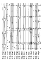
- FIGURE 14(a) shows a transport stream which is input through a terminal 11. user-selected program PCRs have been inserted in this transport stream at the locations P1, P2, P3 and P4.
- This transport stream is applied to the PCR extractor 14, wherein the PCR field detection signal shown in FIGURE 14(b) is generated.
- This PCR field detection signal in synchronous with the transport stream shows the portions of the transport stream where PCRs have been inserted and stays at a low level in the periods when PCRs have been inserted, i.e., for the durations of P1, P2, P3 and P4 of the transport stream shown in FIGURE 14(a).
- This PCR field detection signal is applied to the timing signal generator 16.
- the user-selected program PCRs P1, P2, P3 and P4 inserted in the transport stream shown in FIGURE 14(a) have been extracted as shown in FIGURE 14(c).
- the extracted PCRs are applied to the latchl7 and the counter 19.
- the master timing signal shown in FIGURE 14(d) is generated in the timing signal generator 16 based on the PCR field detection signal shown in FIGURE 14(b).
- This master timing signal is calculated for AND with the mask signal (FIGURE 14(e)) output from the mask signal generator 33 in the mask circuit 34 comprising, for instance, an AND gate and is forced to drop to a low level and masked for the period TL only.
- the master timing signal changes to the signal shown in FIGURE 14 (f).
- the PCRs, as shown in FIGURE 14(c), output from the PCR extractor 14 are latched in the latch 17 by the masked master timing signal,as shown in FIGURE 14(g), and then applied to the subtractor 21.
- the output signal of the AND gate 181 generates a low level pulse at the timing (A) shown in FIGURE 14(h) in the load controller 18.
- the low level pulse shows whether a program has been switched, the power source has been turned ON or a time base has been switched. The pulse is then applied to the load control signal generating counter 186.
- the masked master timing signal is applied to the load control signal counter 186 as a clock, while the output signal of the AND gate 181 is input as a reset signal. That is, this counter 186 is reset when the output signal of the AND gate 181 drops to the low level. Thereafter, when the reset is canceled, the counter counts up successively in every leading edge of the master timing signal which operates as a clock input. So, the output of the load control signal generating counter 186 changes as shown in FIGURE 14(i). The output of this counter 186 is applied to the first and the second load control signal generators 183 and 184.
- the first load timing signal shown in FIGURE 14(j) and the output signal of the load control signal generating counter 186 shown in FIGURE 14(i) are input.
- the first load timing signal shown in FIGURE 14(j) is generated in the timing signal generator 16 based on the PCR field detection signal shown in FIGURE 14(b) and PCRs are loaded on the counter 19 in the low level period.
- the first load control signal generator outputs the signal shown in FIGURE 14(k). This signal is a signal through the first load timing signal only in the period when the output signal of the load control signal generating counter 186 is 0 and is at the high level in the period of other values.
- the second load control signal generator 184 the masked second load timing signal shown in FIGURE 14(1) and the output signal of the load control signal generating counter 186 shown in FIGURE 14(i) are input.
- the second load timing signal shown in FIGURE 14(1) is the signal generated based on the PCR field detection signal shown in FIGURE 14(b) in the timing signal generator 16 and masked by the mask signal in the mask circuit 35 in the same technique as in the mask circuit 34, and is forced at the high level only in the period TL. Further, the load timing of this second load timing signal is to load PCRs on the counter 19 in the low level period.
- the second load control signal generator 184 outputs the signal shown in FIGURE 14(m). This signal passes through the second load timing signal only in the period when the output signal of the load control signal generating counter 186 is 1 and is at the high level.
- the first load control signal shown in FIGURE 14(k) and the second load control signal shown in FIGURE 14(m) are applied to the AND gate 185 and the load control signal shown in FIGURE 14(n) is obtained by the AND operation.
- This load control signal controls the loading operation to the counter 19 and the loading operation to the counter 19 is allowed when this load control signal is at the low level.
- the load control signal is at the low level immediately before the times (B) and (D).
- the outputs of the PCR extractor 14 in this period shown in FIGURE 14(c) are P1 at the time (B) and P3 at the time (D) and these values are loaded on the counter 19.
- the loading operation at the time (B) is the first loading operation. Thereafter the PCR transmitted more than the fixed period of time TL is loaded for the second operation.
- a PCR first transmitted after more than a fixed period of time TL is P3 and this P3 is loaded on the counter 19 immediately before the time (D).
- the values of P1 and P3 loaded on the counter 19 are output immediately after the times (B) and (D) as the counts of the counter 19 as shown in FIGURE 14(o). That is, after outputting P1 which is a value of PCR loaded immediately after the time (B), the counter 19 performs the counting until outputting P3 immediately before the time (D), outputs P3 which is a value of PCR loaded again immediately after the time (D). Thereafter the counting is successively performed.
- the counts of the counter 19 shown in FIGURE 14(o) are latched by the masked master timing signal (see FIGURE 14(f)) in the latch 20, thus change to the signal shown in FIGURE 14(p) and then applied to the subtractor 21.
- the output O of the subtractor 21 passes through the load-pass filter 22 and controls the VCXO 23.
- the VCXO 23 outputs a system clock having the frequency f1 corresponding to the output 0 of the subtractor 21 passed through the low-pass filter 22.
- the transmitter system clock frequency is presented by fM.
- the counter 19 runs under a control of a system clock having frequency f1
- a difference equivalent to a difference between transmitted and received system clock frequencies fM and f1 is generated between the output S3 of the counter 19 immediately before the time (D) and the PCR P3. Therefore, the output of the subtractor 21 takes the value ⁇ K3.
- ⁇ K3 As the value of ⁇ K3 shown by equation (5-4) is an integer, although a value of t1 is too small and a difference fM - f1 between transmitted and received system clock frequencies has a certain amount of value, if the ⁇ K3 satisfies a condition; -1 ⁇ ⁇ K3 ⁇ 1, the ⁇ K3 becomes 0 by operations of omitting the decimal point and less. Therefore, even when PCRs are loaded twice, a difference between transmitted and received system clocks cannot be removed.
- t1 when a difference between transmitted and received system clocks is above a certain level, it is necessary to set t1 so that the ⁇ K3 satisfies a condition; ⁇ K3 ⁇ 1 or ⁇ K3 ⁇ -1.
- the threshold value of this t1 is the period TL which masked the master timing signal and if a difference is calculated first after this period TL is exceeded, a relation; ⁇ K3 ⁇ 0 is obtained.
- This ⁇ K3 is a value resulting from the difference in the transmitted and received system clock frequencies. Therefore, if the VCXO 23 is controlled by passing this ⁇ K3 through the low-pass filter 22, it is possible to bring a system clock frequency obtained from the VCXO 23 to a value close to the transmitter system clock frequency fM.
- FIGURE 15 shows the arrangement of a PLL circuit involved in a sixth embodiment according to the present invention.
- the same reference numerals will be assigned to the same elements as in FIGURES 3 and 11, and different elements will be explained here.
- This embodiment is a combination of the second and the fifth embodiments and provided with a means for loading PCRs twice continuously and skip PCRs for a fixed period of time between the first and second loading operations and means to compensate and normalize a difference between PCRs and counts.
- the timing signal generator 16 generates the master timing signal, the first and the second load timing signals, and the compensation timing signal.
- the master timing signal is applied to the mask signal generator 33 and the first mask circuit 34
- the first load timing signal is applied to the first load control signal generator 183
- the second load timing signal is applied to the second mask circuit 35
- the compensation timing signal is applied to a third mask circuit 36.
- a mask signal is generated from the master timing signal and the output signal of the AND gate of the load controller 18. This mask signal is applied to the first through the third mask circuits 34 - 36.
- the first mask circuit 34 masks the master timing signal according to the mask signal.
- the second mask circuit 35 masks the second load timing signal according to the mask signal.
- the third mask circuit 36 masks the compensation timing signal.
- a difference of PCR and count which is output from the subtractor 21 is applied to the compensator 31.
- the compensator 31 compensates the difference, which is the output of the subtractor 21, to reflect a PCR insertion interval and normalize the difference.
- the masked compensation timing signal rises a pulse synchronizing with the timing to calculate a difference between PCR and count. So, it is possible to obtain a PCR insertion interval by measuring pulse intervals of the masked compensation timing signal in the compensator 31 and compensate a difference, which is the output of the subtractor 21, in accordance with this PCR insertion interval.
- FIGURE 14(a) shows a transport stream which is input through the terminal 11.
- user-selected program PCRs have been inserted at the locations P1, P2, P3 and P4.
- This transport stream is applied to the PCR extractor 14, wherein the PCR field detection signal shown in FIGURE 14(b) is generated.
- This PCR field detection signal in synchronous with the transport stream shows the portions of the transport steam in which PCRs have been inserted and is at the low level in the periods in which PCRS have been inserted, that is, the periods P1, P2, P3 and P4 of the transport stream shown in FIGURE 14(a).
- This PCR field detection signal is applied to the timing signal generator 16.
- the master timing signal shown in FIGURE 16(d) is generated based on the PCR field detection signal shown in FIGURE 16(b).
- This master timing signal is calculated for AND (logical product) with the mask signal (see FIGURE 16(e)) output from the mask signal generator 33 in the mask circuit 34 comprising, for instance, an AND gate and is forced to drop to the low level and masked only for the period TL.
- the master timing signal changes as shown in FIGURE 16(f).
- the masked master timing signal is input as a clock and the output signal of the AND gate 181 is input as a reset signal. That is, this counter 186 is reset when the output signal of the AND gate 181 drops to the low level. Thereafter, when the reset is canceled, the counter performs the counting successively in every leading edge of the master timing signal which operates as a clock input. So, the output of the load control signal generating counter 186 will change as shown in FIGURE 16(i). The output of this counter 186 is applied to the first and the second load control signal generators 183 and 184.
- the first load timing signal shown in FIGURE 16(j) and the output signal of the load control signal generating counter 186 shown in FIGURE 16(i) are applied to the first load control signal generator 183.
- the first load timing signal shown in FIGURE 16(j) is generated based on the PCR field detection signal shown in FIGURE 16(b) in the timing signal generator 16 and has a timing for loading PCR on the counter 19 at a timing when it is at the low level.
- the first load control signal generator 183 outputs the signal shown in FIGURE 16(k). This signal passes through the first load timing signal only in the period when the output signal of the load control signal generating counter 186 is 0 and is at the high level in the period of other values.
- the second load control signal generator 184 the masked second load timing signal shown in FIGURE 16(1) and the output signal of the load control signal generating counter 186 shown in FIGURE 16(i) are input.
- the second load timing signal shown in FIGURE 16(1) is the signal generated based on the PCR field detection signal shown in FIGURE 16(b) in the timing signal generator 16 and masked by the mask signal in the mask circuit 35, and is forced at the high level only in the period TL. Further, this second load timing signal and has a timing for loading PCR on the counter 19 in the period when it is at the low level.
- the second load control signal generator 184 outputs the signal shown in FIGURE 16(m). This signal passes through the second load timing signal only when the output signal of the load control signal generating counter 186 is 1 and is at the high level in the period when it is other values.
- the first load control signal shown in FIGURE 16(k) and the second load control signal shown in FIGURE 16(m) are applied to the AND gate 185 and the load control signal shown in FIGURE 16(n) is obtained as a result of their AND operation.
- This load control signal controls the loading operation to the counter 19 and when this load control signal is at the low level, the loading operation to the counter 19 is allowed.
- the load control signal is at the low level immediately before the times (B) and (D).
- the output of the PCR extractor 14 shown in FIGURE 16(c) in this period are P1 and P3 at the times (B) and (D), respectively and these values are loaded on the counter 19.
- PCR is loaded at the time (B) for the first time. Thereafter, PCR transmitted later more than a fixed period of time TL is loaded for the second time.
- a value of PCR transmitted for the first time more than a fixed period of time TL later is P3 and this P3 is loaded immediately before the time (D).
- the values of P1 and P3 loaded on the counter 19 are output immediately after the times (B) and (D), respectively as the counts of the counter 19 as shown in FIGURE 16(o). That is, after outputting P1, the value of PCR loaded immediately after the time (B), the counter 19 counts up successively until outputting 53 immediately before the time (D) and output P3, the value of PCR loaded again immediately after the time (D) and counts up continuously.
- the output of the counter 19 shown in FIGURE 16(o) is latched by the masked master timing signal (see FIGURE 16(f)) in the latch 20, thus changes to the signal shown in FIGURE 16(p), and then applied to the subtractor 21.
- the VCXO 23 outputs a system clock having frequency f1 corresponding to the output 0 of the compensator 31 passed through the low-pass filter 22.
- the transmitter system clock frequency is presented by fM.
- the counter 19 operates at a system clock having frequency f1
- ⁇ K3 As the value of ⁇ K3 shown by the equation (6-4) is an integer, if the value of tl is too small, a difference between transmitted and received system clock frequencies expressed by fM - f1, if any, figures less than the decimal point is discarded, if the condition; -1 ⁇ ⁇ K3 ⁇ 1 is satisfied. Then the ⁇ K3 becomes 0. So, a difference between transmitted and received system clocks cannot be eliminated even when PCRs are loaded twice.
- This ⁇ K3 takes a value resulting from the difference between the transmitted and received system clock frequencies in the period T1. Further, the output ⁇ K3 of the subtractor 21 involves a time factor tl corresponding to a PCR insertion interval, in addition to the factor of (fM - f1) corresponding to the difference between the transmitted and received system clock frequencies.
- the factor of PCR insertion interval is removed and the output of the subtractor 19 is normalized by calculating the PCR insertion interval and multiplexing the output ⁇ K3 of the subtractor 21 with the reciprocal of the PCR inserting distance calculated as a compensation coefficient in the compensator 31.
- the output of the compensator 31 is shown in FIGURE 16(r). Further, the normalized output ⁇ M3 of the compensator 31 is expressed by the equation (6-5).
- the output ⁇ K3 of the compensator 31 obtained as described above becomes a value depending on only the transmitted and received system clock frequencies. Therefore, when the VCXO 23 is controlled by the ⁇ M3 output from the compensator 31 passed through the low-pass filter 22, it is possible to match the transmitted and received system clock frequencies with each other immediately after the time (D).
- the PCR P3 When the PCR P3 is loaded on the counter 19 after the transmitted and received system clocks have been matched with each other immediately after the time (D), the difference between the PCR and the counter output becomes 0. Also, the phase difference can be removed at the same time. So, it is possible to match the transmitted and received system clock frequencies and phases with each other.
- the output of the subtractor 21 which corresponds to the difference between the PCR and the counter output, is normalized to a value depending on a difference between transmitted and received system clock frequencies as described above, it becomes possible to control the VCXO 23 always accurately.
- the PLL circuit in this embodiment it is possible to detect a difference between transmitted and received system clock frequencies positively at the second loading operation when more than a fixed period of time is left between the first and the second loading operations for consecutively loading twice the PCRs on the counter.
- the VCXO 23 is controllable by the difference between the transmitted and received system clock frequencies, it is possible to nearly match the transmitted and received system clock frequencies and phases with each other at the second loading operation. Thus the time required for locking the received frequency and the phase of the system clock is reduced.
- the VCXO 23 can be accurately controlled.
- the sixth embodiment described above is a combination of the second embodiment and the fifth embodiment, it is also possible to construct another embodiment by combining the third and the fifth embodiments by replacing the compensator by the arrangement described in the third embodiment.
- FIGURE 17 shows a seventh embodiment of the PLL circuit according to the present invention. This embodiment concerns to a software-based processing using the techniques shown in the first through the sixth embodiments applied to the CPU.
- FIGURE 17 a transport stream input through a terminal 41 is applied to a PCR extractor 45.
- a program selection signal input through a terminal 42 is applied to the PCR extractor 45 and a program switching signal generator 46.
- the program selection signal showing a user-selected program is converted to a program switching signal to generate a pulse at the program switching in the program switching signal generator 46.
- the PCR extractor 45 extracts a PCR for programs selected from the transport stream input through the terminal 41 according to the program selection signal, supplies the PCR into a CPU 50 and a counter 47, and at the same time, generates a PCR field detection signal showing locations of the transport stream where the selected program PCRs have been placed and applies the detection signal to the CPU 50 to generate a time base switching signal showing the completion of a time base switching for applying the signal to an AND gate 49.
- the arrangement of this PCR extractor 45 is the same as that of the PCR extractor 14 of a conventional PLL circuit shown in FIGURE 20.
- the time base switching signal output from the PCR extractor 45, the program switching signal output from the program switching signal generator 46 and a power ON reset signal which is input through a terminal 43 are applied to the AND gate 49.
- This AND gate 49 performs an AND operation of a time base switching signal, the program switching signal and the power ON reset signal.
- the output signal of this AND gate 49 shows whether a program has been switched, a time base has been switched or a power source has been turned ON and is applied to the CPU 50.
- the counter 47 loads the PCRs output from the PCR extractor 45 under a control of a load control signal output from the CPU 50, counts up by a system clock output from a VCXO 48 and applies the count to the CPU 50.
- the CPU 50 captures the PCR field detection signal, the PCRs, the counts of the counter 47 and the counts of the AND gate 49 to generate a voltage control signal of the VCXO 48 and a load control signal of the counter 47.
- the VCXO 48 generates a system clock of frequency corresponding to the voltage control signal output from the CPU 50 and this system clock is applied to the counter 47 and a terminal 44.
- the system clock applied to the terminal 44 is used for various processing at the receiver.
- a software-based processing is carried out for consecutively loading twice the PCR, as shown in the sixth embodiment, skipping the PCRs for a fixed period of time between the first and the second loading operations and compensating to normalize the difference between the PCR and the counter output.
- the software-based processing performed in the CPU 50 will be explained in referring to a flowchart shown in FIGURE 18.
- the CPU 50 executes the step S2 and captures the PCRs output from the PCR extractor 45.
- the decision step S3 capturing the output signal from the AND gate 49, the CPU 50 judges whether a program has been switched, a time base has been switched or the power source has been turned ON.
- the CPU 50 captures PCR and executes the step S4 according to the result of judgment in the decision step S3.
- the CPU 50 gives an instruction to allow the loading operation (load control signal) to the counter 4 for loading PCR on the counter 47. This is the first loading operation of PCR on the counter 47.
- the CPU 50 After loading the PCR on the counter 47, the CPU 50 executes the decision otep S5. In the decision step S5, the CPU 50 judges if a difference between the first transmitted PCR and a counter output has been calculated immediately after the program switching, the time base switching or the power source turn-ON.
- step S7 is executed.
- the difference between the PCR and the output of the counter 47 is calculated according to the PCR field detection signal which is output from the PCR extractor 45.
- the difference between the PCR and the output of the counter 47 is normalized in the step S8.
- the normalization process includes a process of compensating the difference between the PCR and the output of the counter 47 according to the PCR insertion interval.
- the normalized difference between the PCR and the output of the counter 47 is low-pass filtered in the step S9.
- the normalized and low-pass filtered difference between the PCR and the output of the counter 47 is judged in the decision step S10 as to whether the difference between the second PCR and the output of the counter 47 has been calculated immediately after the program switching, the time base switching or the power source turn-ON.
- step S12 the output of the low-pass filter is applied to the VCXO 48 for the voltage control of the VCXO 48.
- the second PCR is calculated. Then, the judgment in the decision step S3 is performed. In this case, the judgment results to "NO", as it is not immediately after the program switching, the time base switching or the power source turned ON and the decision step S5 is executed.
- step S5 The judgment in the decision step S5 is "YES" and the step S6 is executed as a difference between the first transmitted PCR and the output of the counter 47 has been calculated immediately after the program switching, the time base switching or the power source turned ON after the second PCR has been captured.
- the period left between the first and the second loading operations is presented by T1
- the threshold value of the period for skipping the PCR for the period left between the first and the second loading operations is presented by TL.
- the step 6 when skipping the transmitted PCR for until the period T1 becomes larger than or equal to threshold value of the period TL (i.e., T1 ⁇ TL).
- T1 ⁇ TL threshold value of the period TL
- the decision step S10 is "YES" and the step S11 is executed as a difference between the second PCR and the output of the counter 47 has been calculated immediately after the program switching, the time base switching or the power source turned ON.
- the CPU 50 gives an instruction (load control signal) to allow the loading the PCRs to the counter 47, Thus the second lqading operation of the PCRs to the counter 47 is performed.
- the output of the low-pass filter is applied to the VCXO 48 in the step S12.
- the processing After outputting the output of the low-pass filter, the processing turns back to the step S2, and thus the third capturing operation of the PCR is carried out. Thereafter, the operation forwards to the judgment in the decision step S3.
- the judgment in the decision step S5 is performed.
- the result of judgment in the decision step S5 is "NO”.
- a series of processing the steps S7, S8 and S9 are performed.
- the judgment in the decision step S10 is performed.
- the step S12 is executed.
- a series of the steps S2, S7, S8, S9 and S12 are repeatedly carried out for calculating the difference between the PCR and the output of the counter 47, normalizing the difference and outputting the low-pass filtered difference to the VCXO 48.
- the PLL circuit described above it is possible to perform the similar operations as in the sixth embodiment by performing the software-based processing described above in the CPU 50. So, the similar effects as in the sixth embodiment can be achieved. That is, it is possible to reduce a time required for locking the received frequency and phase of the system clock and accurately control the VCXO.
- the software process in the CPU 50 can be modified in various forms and also, it is possible to perform the operations similar to those described in the first through the fifth embodiments.
- the present invention can provide an extremely preferable PLL circuit and method.
Landscapes
- Engineering & Computer Science (AREA)
- Signal Processing (AREA)
- Computer Networks & Wireless Communication (AREA)
- Multimedia (AREA)
- Synchronisation In Digital Transmission Systems (AREA)
- Stabilization Of Oscillater, Synchronisation, Frequency Synthesizers (AREA)
- Medicines That Contain Protein Lipid Enzymes And Other Medicines (AREA)
- Synchronizing For Television (AREA)
- Digital Transmission Methods That Use Modulated Carrier Waves (AREA)
- Superheterodyne Receivers (AREA)
Applications Claiming Priority (2)
| Application Number | Priority Date | Filing Date | Title |
|---|---|---|---|
| JP114016/95 | 1995-04-14 | ||
| JP11401695A JPH08288880A (ja) | 1995-04-14 | 1995-04-14 | Pll回路及び方式 |
Publications (1)
| Publication Number | Publication Date |
|---|---|
| EP0738054A2 true EP0738054A2 (fr) | 1996-10-16 |
Family
ID=14626947
Family Applications (1)
| Application Number | Title | Priority Date | Filing Date |
|---|---|---|---|
| EP96302626A Withdrawn EP0738054A2 (fr) | 1995-04-14 | 1996-04-15 | Circuit PLL pour récepteur de radiodiffusion numérique |
Country Status (5)
| Country | Link |
|---|---|
| US (1) | US5768326A (fr) |
| EP (1) | EP0738054A2 (fr) |
| JP (1) | JPH08288880A (fr) |
| KR (1) | KR100197312B1 (fr) |
| CA (1) | CA2174197A1 (fr) |
Families Citing this family (16)
| Publication number | Priority date | Publication date | Assignee | Title |
|---|---|---|---|---|
| KR100190996B1 (ko) * | 1995-08-09 | 1999-06-15 | 이계철 | 위상 동기회로 |
| US6233256B1 (en) * | 1996-03-13 | 2001-05-15 | Sarnoff Corporation | Method and apparatus for analyzing and monitoring packet streams |
| EP0836282B1 (fr) * | 1996-10-08 | 2002-06-12 | Sony Corporation | Appareil et procédé de réception et boucle à verrouillage de phase |
| KR100241325B1 (ko) * | 1996-11-06 | 2000-02-01 | 윤종용 | 엠펙-2 디코더의 클럭 복원 장치 및 그 복원 방법 |
| US6195403B1 (en) * | 1997-09-26 | 2001-02-27 | International Business Machines Corporation | Pulse generator for a voltage controlled oscillator |
| US6356567B2 (en) * | 1997-09-26 | 2002-03-12 | International Business Machines Corporation | Embedded clock recovery and difference filtering for an MPEG-2 compliant transport stream |
| US8306170B2 (en) * | 1998-03-31 | 2012-11-06 | International Business Machines Corporation | Digital audio/video clock recovery algorithm |
| US6400930B1 (en) * | 1998-11-06 | 2002-06-04 | Dspc Israel, Ltd. | Frequency tuning for radio transceivers |
| DE19946502C1 (de) * | 1999-09-28 | 2001-05-23 | Siemens Ag | Schaltungsanordnung zum Erzeugen eines zu Referenztaktsignalen frequenzsynchronen Taktsignals |
| US6429902B1 (en) * | 1999-12-07 | 2002-08-06 | Lsi Logic Corporation | Method and apparatus for audio and video end-to-end synchronization |
| JP2004015318A (ja) * | 2002-06-05 | 2004-01-15 | Fujitsu Ltd | システムクロック同期手段を有する情報伝送システムおよびその情報伝送装置 |
| KR100449742B1 (ko) * | 2002-10-01 | 2004-09-22 | 삼성전자주식회사 | 멀티미디어 방송 송수신 장치 및 방법 |
| US8284886B2 (en) * | 2003-01-17 | 2012-10-09 | Texas Instruments Incorporated | Radio frequency built-in self test for quality monitoring of local oscillator and transmitter |
| WO2008129816A1 (fr) * | 2007-03-28 | 2008-10-30 | Panasonic Corporation | Procédé de synchronisation d'horloge |
| JP5124755B2 (ja) * | 2007-11-13 | 2013-01-23 | 石川県 | 画像撮影システム |
| JP6603437B2 (ja) * | 2017-03-27 | 2019-11-06 | 株式会社日立国際電気 | 放送波同期信号変換装置 |
Family Cites Families (2)
| Publication number | Priority date | Publication date | Assignee | Title |
|---|---|---|---|---|
| US5287182A (en) * | 1992-07-02 | 1994-02-15 | At&T Bell Laboratories | Timing recovery for variable bit-rate video on asynchronous transfer mode (ATM) networks |
| US5543853A (en) * | 1995-01-19 | 1996-08-06 | At&T Corp. | Encoder/decoder buffer control for variable bit-rate channel |
-
1995
- 1995-04-14 JP JP11401695A patent/JPH08288880A/ja active Pending
-
1996
- 1996-04-12 US US08/631,198 patent/US5768326A/en not_active Expired - Fee Related
- 1996-04-13 KR KR1019960011188A patent/KR100197312B1/ko not_active Expired - Fee Related
- 1996-04-15 CA CA002174197A patent/CA2174197A1/fr not_active Abandoned
- 1996-04-15 EP EP96302626A patent/EP0738054A2/fr not_active Withdrawn
Also Published As
| Publication number | Publication date |
|---|---|
| JPH08288880A (ja) | 1996-11-01 |
| CA2174197A1 (fr) | 1996-10-15 |
| US5768326A (en) | 1998-06-16 |
| KR960039657A (ko) | 1996-11-25 |
| KR100197312B1 (ko) | 1999-06-15 |
Similar Documents
| Publication | Publication Date | Title |
|---|---|---|
| EP0738054A2 (fr) | Circuit PLL pour récepteur de radiodiffusion numérique | |
| US3984624A (en) | Video system for conveying digital and analog information | |
| JP3964041B2 (ja) | 視聴チャンネル判定装置 | |
| EP0703713A2 (fr) | Dispositif pour la réception de paquets | |
| DK154386B (da) | Fremgangsmaade og apparat til at tidslaase en mikroprocessor til synkroniseringsimpulserne i et videosignal | |
| JP3694529B2 (ja) | ディジタルテレビジョンの同期化 | |
| KR0152040B1 (ko) | 심볼타이밍복구 및 동기신호검출을 이용한 고선명텔레비젼/엔티에스씨 공용수신방법 및 그 장치 | |
| US5832256A (en) | System clock recovery apparatus for MPEG decoding system | |
| US5483538A (en) | Audio frame synchronization for embedded audio demultiplexers | |
| US6545725B1 (en) | Apparatus for identifying standard and non-standard video signals | |
| EP0793357A2 (fr) | Correlateur et dispositif de poursuite synchrone pour des récepteurs à spectre étalé | |
| US4198659A (en) | Vertical synchronizing signal detector for television video signal reception | |
| US20050046744A1 (en) | Method for transmitting video signals | |
| EP0767589B1 (fr) | Générateur de signal d'horloge | |
| JPH0936833A (ja) | 多重化端局装置 | |
| JPH08275074A (ja) | デジタル・クロック発生装置 | |
| JP2001177401A (ja) | 位相同期回路 | |
| KR0128046Y1 (ko) | 방송 프로그램 예약 시스템에서의 데이터 복원회로 | |
| JP3523147B2 (ja) | 標準・非標準信号判定回路 | |
| WO1988003338A1 (fr) | Procede et dispositif pour recevoir des signaux analogiques modules en frequence avec traitement numerique | |
| JPH09231202A (ja) | 相関器 | |
| KR930006484B1 (ko) | 임펄스 노이즈 발생장치의 윈도우 펄스 발생회로 및 방법 | |
| JPH07264108A (ja) | 伝送装置 | |
| KR0157547B1 (ko) | 트랜스포트 디멀티플렉서의 동기복구장치 | |
| JP3118938B2 (ja) | スペクトラム拡散通信用復調装置 |
Legal Events
| Date | Code | Title | Description |
|---|---|---|---|
| PUAI | Public reference made under article 153(3) epc to a published international application that has entered the european phase |
Free format text: ORIGINAL CODE: 0009012 |
|
| 17P | Request for examination filed |
Effective date: 19960509 |
|
| AK | Designated contracting states |
Kind code of ref document: A2 Designated state(s): DE FR GB NL |
|
| STAA | Information on the status of an ep patent application or granted ep patent |
Free format text: STATUS: THE APPLICATION HAS BEEN WITHDRAWN |
|
| 18W | Application withdrawn |
Withdrawal date: 19990816 |