EP0738599B1 - Tête d'enregistrement à jet d'encre et procédé pour sa fabrication - Google Patents
Tête d'enregistrement à jet d'encre et procédé pour sa fabrication Download PDFInfo
- Publication number
- EP0738599B1 EP0738599B1 EP96106204A EP96106204A EP0738599B1 EP 0738599 B1 EP0738599 B1 EP 0738599B1 EP 96106204 A EP96106204 A EP 96106204A EP 96106204 A EP96106204 A EP 96106204A EP 0738599 B1 EP0738599 B1 EP 0738599B1
- Authority
- EP
- European Patent Office
- Prior art keywords
- film
- recording head
- ink jet
- jet recording
- head according
- Prior art date
- Legal status (The legal status is an assumption and is not a legal conclusion. Google has not performed a legal analysis and makes no representation as to the accuracy of the status listed.)
- Expired - Lifetime
Links
Images


Classifications
-
- B—PERFORMING OPERATIONS; TRANSPORTING
- B41—PRINTING; LINING MACHINES; TYPEWRITERS; STAMPS
- B41J—TYPEWRITERS; SELECTIVE PRINTING MECHANISMS, i.e. MECHANISMS PRINTING OTHERWISE THAN FROM A FORME; CORRECTION OF TYPOGRAPHICAL ERRORS
- B41J2/00—Typewriters or selective printing mechanisms characterised by the printing or marking process for which they are designed
- B41J2/005—Typewriters or selective printing mechanisms characterised by the printing or marking process for which they are designed characterised by bringing liquid or particles selectively into contact with a printing material
- B41J2/01—Ink jet
- B41J2/135—Nozzles
- B41J2/16—Production of nozzles
- B41J2/1621—Manufacturing processes
- B41J2/1626—Manufacturing processes etching
- B41J2/1629—Manufacturing processes etching wet etching
-
- B—PERFORMING OPERATIONS; TRANSPORTING
- B41—PRINTING; LINING MACHINES; TYPEWRITERS; STAMPS
- B41J—TYPEWRITERS; SELECTIVE PRINTING MECHANISMS, i.e. MECHANISMS PRINTING OTHERWISE THAN FROM A FORME; CORRECTION OF TYPOGRAPHICAL ERRORS
- B41J2/00—Typewriters or selective printing mechanisms characterised by the printing or marking process for which they are designed
- B41J2/005—Typewriters or selective printing mechanisms characterised by the printing or marking process for which they are designed characterised by bringing liquid or particles selectively into contact with a printing material
- B41J2/01—Ink jet
- B41J2/135—Nozzles
- B41J2/14—Structure thereof only for on-demand ink jet heads
- B41J2/14201—Structure of print heads with piezoelectric elements
- B41J2/14233—Structure of print heads with piezoelectric elements of film type, deformed by bending and disposed on a diaphragm
-
- B—PERFORMING OPERATIONS; TRANSPORTING
- B41—PRINTING; LINING MACHINES; TYPEWRITERS; STAMPS
- B41J—TYPEWRITERS; SELECTIVE PRINTING MECHANISMS, i.e. MECHANISMS PRINTING OTHERWISE THAN FROM A FORME; CORRECTION OF TYPOGRAPHICAL ERRORS
- B41J2/00—Typewriters or selective printing mechanisms characterised by the printing or marking process for which they are designed
- B41J2/005—Typewriters or selective printing mechanisms characterised by the printing or marking process for which they are designed characterised by bringing liquid or particles selectively into contact with a printing material
- B41J2/01—Ink jet
- B41J2/135—Nozzles
- B41J2/16—Production of nozzles
- B41J2/1607—Production of print heads with piezoelectric elements
- B41J2/161—Production of print heads with piezoelectric elements of film type, deformed by bending and disposed on a diaphragm
-
- B—PERFORMING OPERATIONS; TRANSPORTING
- B41—PRINTING; LINING MACHINES; TYPEWRITERS; STAMPS
- B41J—TYPEWRITERS; SELECTIVE PRINTING MECHANISMS, i.e. MECHANISMS PRINTING OTHERWISE THAN FROM A FORME; CORRECTION OF TYPOGRAPHICAL ERRORS
- B41J2/00—Typewriters or selective printing mechanisms characterised by the printing or marking process for which they are designed
- B41J2/005—Typewriters or selective printing mechanisms characterised by the printing or marking process for which they are designed characterised by bringing liquid or particles selectively into contact with a printing material
- B41J2/01—Ink jet
- B41J2/135—Nozzles
- B41J2/16—Production of nozzles
- B41J2/1621—Manufacturing processes
- B41J2/1623—Manufacturing processes bonding and adhesion
-
- B—PERFORMING OPERATIONS; TRANSPORTING
- B41—PRINTING; LINING MACHINES; TYPEWRITERS; STAMPS
- B41J—TYPEWRITERS; SELECTIVE PRINTING MECHANISMS, i.e. MECHANISMS PRINTING OTHERWISE THAN FROM A FORME; CORRECTION OF TYPOGRAPHICAL ERRORS
- B41J2/00—Typewriters or selective printing mechanisms characterised by the printing or marking process for which they are designed
- B41J2/005—Typewriters or selective printing mechanisms characterised by the printing or marking process for which they are designed characterised by bringing liquid or particles selectively into contact with a printing material
- B41J2/01—Ink jet
- B41J2/135—Nozzles
- B41J2/16—Production of nozzles
- B41J2/1621—Manufacturing processes
- B41J2/1631—Manufacturing processes photolithography
-
- B—PERFORMING OPERATIONS; TRANSPORTING
- B41—PRINTING; LINING MACHINES; TYPEWRITERS; STAMPS
- B41J—TYPEWRITERS; SELECTIVE PRINTING MECHANISMS, i.e. MECHANISMS PRINTING OTHERWISE THAN FROM A FORME; CORRECTION OF TYPOGRAPHICAL ERRORS
- B41J2/00—Typewriters or selective printing mechanisms characterised by the printing or marking process for which they are designed
- B41J2/005—Typewriters or selective printing mechanisms characterised by the printing or marking process for which they are designed characterised by bringing liquid or particles selectively into contact with a printing material
- B41J2/01—Ink jet
- B41J2/135—Nozzles
- B41J2/16—Production of nozzles
- B41J2/1621—Manufacturing processes
- B41J2/1632—Manufacturing processes machining
-
- B—PERFORMING OPERATIONS; TRANSPORTING
- B41—PRINTING; LINING MACHINES; TYPEWRITERS; STAMPS
- B41J—TYPEWRITERS; SELECTIVE PRINTING MECHANISMS, i.e. MECHANISMS PRINTING OTHERWISE THAN FROM A FORME; CORRECTION OF TYPOGRAPHICAL ERRORS
- B41J2/00—Typewriters or selective printing mechanisms characterised by the printing or marking process for which they are designed
- B41J2/005—Typewriters or selective printing mechanisms characterised by the printing or marking process for which they are designed characterised by bringing liquid or particles selectively into contact with a printing material
- B41J2/01—Ink jet
- B41J2/135—Nozzles
- B41J2/16—Production of nozzles
- B41J2/1621—Manufacturing processes
- B41J2/1635—Manufacturing processes dividing the wafer into individual chips
-
- B—PERFORMING OPERATIONS; TRANSPORTING
- B41—PRINTING; LINING MACHINES; TYPEWRITERS; STAMPS
- B41J—TYPEWRITERS; SELECTIVE PRINTING MECHANISMS, i.e. MECHANISMS PRINTING OTHERWISE THAN FROM A FORME; CORRECTION OF TYPOGRAPHICAL ERRORS
- B41J2/00—Typewriters or selective printing mechanisms characterised by the printing or marking process for which they are designed
- B41J2/005—Typewriters or selective printing mechanisms characterised by the printing or marking process for which they are designed characterised by bringing liquid or particles selectively into contact with a printing material
- B41J2/01—Ink jet
- B41J2/135—Nozzles
- B41J2/16—Production of nozzles
- B41J2/1621—Manufacturing processes
- B41J2/164—Manufacturing processes thin film formation
- B41J2/1646—Manufacturing processes thin film formation thin film formation by sputtering
-
- B—PERFORMING OPERATIONS; TRANSPORTING
- B41—PRINTING; LINING MACHINES; TYPEWRITERS; STAMPS
- B41J—TYPEWRITERS; SELECTIVE PRINTING MECHANISMS, i.e. MECHANISMS PRINTING OTHERWISE THAN FROM A FORME; CORRECTION OF TYPOGRAPHICAL ERRORS
- B41J2/00—Typewriters or selective printing mechanisms characterised by the printing or marking process for which they are designed
- B41J2/005—Typewriters or selective printing mechanisms characterised by the printing or marking process for which they are designed characterised by bringing liquid or particles selectively into contact with a printing material
- B41J2/01—Ink jet
- B41J2/135—Nozzles
- B41J2/14—Structure thereof only for on-demand ink jet heads
- B41J2002/14387—Front shooter
-
- Y—GENERAL TAGGING OF NEW TECHNOLOGICAL DEVELOPMENTS; GENERAL TAGGING OF CROSS-SECTIONAL TECHNOLOGIES SPANNING OVER SEVERAL SECTIONS OF THE IPC; TECHNICAL SUBJECTS COVERED BY FORMER USPC CROSS-REFERENCE ART COLLECTIONS [XRACs] AND DIGESTS
- Y10—TECHNICAL SUBJECTS COVERED BY FORMER USPC
- Y10T—TECHNICAL SUBJECTS COVERED BY FORMER US CLASSIFICATION
- Y10T29/00—Metal working
- Y10T29/42—Piezoelectric device making
Definitions
- the present invention relates to an ink jet recording head and a method of producing same.
- ink jet recording heads There are two types of ink jet recording heads, i.e., the piezoelectric vibration type in which ink is pressurized by mechanically deforming a pressure chamber, and the bubble jet type in which a heating element is disposed in a pressure chamber and ink is pressurized by an air bubble produced by heat of the heating element.
- Ink jet recording heads of the piezoelectric vibration type are classified into two categories, a first recording head using a piezoelectric vibrator which is axially deformed, and a second recording head using a piezoelectric vibrator which conducts flexural displacement.
- the first recording head can be driven at a high speed and performs recording at a high density, but requires a cutting operation for producing the piezoelectric vibrator, and a three-dimensional assembly operation for fixing the piezoelectric vibrator to the pressure chamber, thereby producing a problem in that an increased number of production steps are necessary.
- the piezoelectric vibrator has a membrane-like shape, and hence can be formed by baking the piezoelectric vibrator integrally with an elastic film constituting the pressure chamber. Consequently, the second recording head has a reduced number of production steps.
- the second recording head requires an area of a size sufficient to conduct flexural vibration so that the pressure chamber has a large width, thereby reducing the arrangement density.
- Japanese Patent Publication (Kokai) No. HEI5-504740 discloses an ink jet recording head comprising: a substrate in which pressure chambers are formed in a single-crystal silicon substrate of a (110) lattice plane; and a nozzle plate in which a plurality of nozzle openings communicating with the pressure chambers are formed and which is fixed to one face of the substrate.
- the other face of the substrate is formed as a membrane which is elastically deformable.
- a driving portion is integrally disposed by forming a piezoelectric film on the surface of the membrane by a film formation method. The driving portion conducts flexural vibration so as to pressurize ink in the pressure chambers, thereby ejecting ink drops from the nozzle openings.
- the pressure chambers, ink supply ports attached to the chambers, and a reservoir are formed by conducting anisotropic etching on a single-crystal silicon wafer. Because of the characteristics of anisotropic etching, the pressure chambers are obliged to be arranged along a ⁇ 111> lattice orientation of the single-crystal silicon wafer. This causes the wall face of the reservoir for supplying ink to the pressure chambers, to be formed on a (110) plane which is perpendicular to the ⁇ 111> lattice orientation. However, it is very difficult to form the (110) plane by conducting anisotropic etching on a single-crystal silicon substrate. Therefore, a technique in which a wall face defining a reservoir is etched so as to be approximated by a continuum of minute (111) planes is employed.
- a nozzle plate which closes one face of each pressure chamber is elastically contacted with and sealed by a capping member for preventing the flow paths from clogging, and rubbed with a cleaning member which is made of an elastic material such as rubber. Consequently, the nozzle plate must have a mechanical strength which can endure such operations.
- a metal plate member constituting the nozzle plate must have a thickness of 80 ⁇ m or more.
- nozzle openings which can eject ink drops satisfying the above-mentioned requirements have a diameter of about 30 ⁇ m on the ink ejection side.
- the diameter of nozzle openings on the pressure chamber side must be at least 70 ⁇ m, preferably about 90 ⁇ m.
- a signal must be supplied to the driving portion without impeding the vibrating operation. Therefore, it is impossible to directly connect a cable to the driving portion.
- a structure must be employed in which a lead pattern elongating to the driving portion is formed on the surface of a vibrating plate and a cable is connected to the lead pattern at a position which is separated from the vibrating region.
- the driving portion is formed by the above-mentioned film formation method, the level difference between the driving portion and the lead pattern must be made as small as possible so as to ensure the connection therebetween. Therefore, a countermeasure is taken in the following manner.
- the piezoelectric film constituting the driving portion is extended to the region where the lead pattern is to be formed, so as to serve as an insulating film for insulating a lower electrode. Thereafter, a lead pattern is formed on the surface of the piezoelectric film by vapor deposition or the like.
- this countermeasure has the following disadvantage. An electrostatic capacity of a value which is negligible in the view point of transmission of a signal is produced between upper and lower electrodes in the wiring region. This occurs because the piezoelectric film has originally a high specific dielectric constant and is very thin.
- the extra electrostatic capacity produces problems such as the apparent power is increased and the driving circuit is required to have a large current capacity, and that, when a voltage is applied to the lead pattern, piezoelectric displacement or heat generation is caused although the region is a wiring region, whereby the lead pattern formed on the surface is broken or the film is stripped.
- JP-A-06 055 733 discloses an ink jet recording head having pressure chambers arranged in a single crystal-silicon substrate of a (110) lattice plane.
- the pressure chambers are arranged in a row wherein the pressure chambers are defined in the substrate by vertical crystal faces of (111) orientation.
- WO-A-9 322 140 and corresponding US-A-5 530 465 also disclose pressure chambers for an ink jet recording head being arranged in a row in a single crystal-silicon substrate of a (110) lattice plane.
- the pressure chambers are defined by walls of the substrate oriented perpendicular to the substrate surface in either ⁇ l 12> or ⁇ l 12> direction.
- pressure chambers are arranged in a single crystal-silicon substrate of a (110) lattice plane.
- the pressure chambers are arranged in a row extending along a ⁇ 112> lattice orientation or a lattice orientation equivalent to the ⁇ 112> lattice orientation.
- the present invention may provide for an ink jet recording head using a single-crystal silicon substrate which allows the size of the ink reservoir to be reduced to a value that enables the printing function.
- the ink jet head comprises: a nozzle plate in which a plurality of nozzle openings are formed; a flow path substrate comprising a reservoir to which ink is externally supplied, and a plurality of pressure chambers which are connected to the reservoir via an ink supply port and which respectively communicate with the nozzle openings; an elastic film which pressurizes ink in the pressure chambers; and driving means located at a position opposing the respective pressure chamber for causing the elastic film to conduct flexural deformation, wherein the pressure chambers are arranged in a single-crystal silicon substrate of a (110) lattice plane and in arow extending along a ⁇ 112> or equivalent lattice orientation, and a nozzle connecting portion is formed in a region opposing the nozzle openings, the nozzle connecting portion being wider than the other region.
- the present invention may provide for an ink jet recording head in which the pressure chambers can be arranged at a high density while preventing crosstalk from occurring, and the pressure chambers and the nozzle openings are smoothly joined to each other so that ink drops are stably ejected.
- the ink jet head also comprises a nozzle plate in which a plurality of nozzle openings are formed; a flow path substrate comprising a reservoir to which ink is externally supplied, and a plurality of pressure chambers which are connected to the reservoir via an ink supply port and which respectively communicate with the nozzle openings; an elastic film which pressurizes ink in the pressure chambers; and driving means located at a position opposing the respective pressure chamber for causing the elastic film to conduct flexural deformation, wherein the ink jet head further comprises on a surface of the elastic film: a lower electrode; a piezoelectric film formed in a region opposing the respective pressure chamber; a second film having a composition different than that of the piezoelectric film formed in a wiring region for supplying a driving signal to the piezoelectric film, the second film having a dielectric constant and piezoelectric properties which are lower than those of the piezoelectric film; an upper electrode formed on a surface of the piezoelectric film; and a lead pattern
- the present invention may provide for an ink jet recording head in which the capacitance of a wiring region can be made as small as possible so that the load of a driving circuit is reduced, and the possibility of breakage in the wiring region can be made as low as possible.
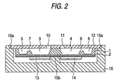
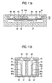
- FIGS. 1 and 2 show an embodiment of the invention.
- the reference numeral 1 designates an ink pressure chamber substrate which is formed by etching a single-crystal silicon substrate.
- the top surface of the substrate is used as an opening face 9.
- a plurality of rows or, in the embodiment, two rows of pressure chambers 3, 3, ..., and 4, 4, ... which are arranged in a staggered manner, reservoirs 5 and 6 which supply ink to the pressure chambers, and ink supply ports 7 and 8 through which the pressure chambers 3 and 4 communicate with the reservoirs 5 and 6 are formed in such a manner that a membrane portion 2 is formed on the back face.
- a nozzle plate 12 is fixed to the opening face 9.
- nozzle openings 10 and 11 are formed so as to communicate with one end of a respective one of the pressure chambers 3 and 4.
- Piezoelectric films 13 and 14 (see Fig. 2) formed by a film formation method are disposed on the back face.
- the ink pressure chamber substrate 1 and the nozzle plate 12 are integrally fixed to each other so as to attain the liquid-tightness, and are housed in a holder 15 having supporting parts 15a and 15b which support the peripheral and center portions, thereby configuring a recording head.
- 17 designates a flexible cable through which a driving signal is supplied to the piezoelectric films 13 and 14.
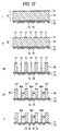
- FIG. 3a is a plan view showing an embodiment of the flow path substrate
- FIG. 3b is a view showing a sectional structure.
- 20 designates a wafer of a single-crystal silicon substrate which is cut so that the surface is a (110) lattice plane.
- ink reservoirs 21, 22, and 23 are formed in the side and center portions, and pressure chambers 24 and 25 are formed between the ink reservoirs or in two rows.
- ink supply ports 26 and 27 or 28 and 29 for receiving ink from the reservoirs 21 and 23 or 22 and 23 which are positioned at both the sides of the row are formed.
- Ink introducing ports 30, 31, and 32 for receiving ink from an external ink tank are opened at ends of the ink reservoirs 21, 22, and 23.
- a base material 42 is prepared wherein an SiO 2 layer 41 of a thickness of about 1 ⁇ m is formed by the thermal oxidation method or the like on the entire surface of a single-crystal silicon substrate 40 which is cut so that the surface is (110).
- the SiO 2 layer 41 serves as an insulating film for a driving portion which will be formed thereon, and also as an etching protective film for a process of etching the single-crystal silicon substrate 40.
- a film of zirconia (Zr) is formed on the surface of the SiO 2 layer 41 by sputtering, and the film is subjected to thermal oxidation, thereby forming an elastic film 43 which has a thickness of 0.8 ⁇ m and is made of zirconium oxide.
- the elastic film 43 made of zirconium oxide has a large Young's modulus so that distortion of a piezoelectric film 44 which will be described later is converted into flexural displacement at high efficiency.
- a film of platinum (Pt) of a thickness of about 0.2 ⁇ m is formed by sputtering on the surface of the elastic film 43, thereby forming a lower electrode 45.
- a film 46 (see FIG.
- the upper electrode 47, the piezoelectric film 46, and the lower electrode 45 are patterned so as to correspond to the arrangement positions of the pressure chambers 24 and 25, thereby forming a driving portion 50.
- This patterning is determined so that the arrangement of the pressure chambers 24 and 25 is directed along a lattice orientation of a ⁇ -1-1-2> zone axis in which zone planes are a (1-1-1) plane and a (110) plane, or a ⁇ 112> lattice orientation which is equivalent to the orientation (in the description of embodiments, a crystal lattice is denoted by enclosing indices by curly brackets, for example, (110), a lattice orientation is denoted by enclosing indices by angle brackets, for example, ⁇ 110>, and 1-bar of a unit cell is indicated as -1).
- the upper electrode 47 is patterned so as to serve also as lead conductors which are independently taken out in correspondence with the pressure chambers 24 and 25 and used as portions to be connected with a driving circuit.
- the piezoelectric film 46 it is not essential to form the piezoelectric film 46 as divided films respectively independently corresponding to the pressure chambers 24 and 25.
- the piezoelectric film 46 is divided into portions which are independently provided for the respective pressure chambers, however, a large amount of flexural displacement occurs, as described later. Therefore, the division of the piezoelectric film is preferable.
- the lower electrode 45 functions as a common electrode, it is preferable not to divide the lower electrode in the patterning.
- the patterning may be conducted each time when one layer is formed (Step II).
- Photoresist layers 48 and 49 are formed so that the arrangement of the pressure chambers 24 and 25 is directed along a lattice orientation of a ⁇ -1-1-2> zone axis in which zone planes are a (1-1-1) plane and a (110) plane, or a ⁇ 112> lattice orientation which has an equivalent orientation (Step III).
- the SiO 2 layer 41 is removed by using a hydrofluoric acid buffer solution in which hydrofluoric acid and ammonium fluoride are mixed in proportions of 1 : 6, so as to pattern a window 51 for anisotropic etching.
- the photoresist layer 49 for the regions of the SiO 2 layer where the ink supply ports 26, 27, 28, and 29 are to be formed is subjected to so-called multiple exposure in which the photoresist layer is again exposed to light.
- Half-etching is then conducted for about 5 min. by using the hydrofluoric acid buffer solution so that the thickness of the SiO 2 layer below the photoresist layer 49 is reduced to about 0.5 ⁇ m (Step IV).
- the base material 42 is immersed into a 10% by weight solution of potassium hydroxide heated to about 80°C, thereby executing anisotropic etching.
- side walls 24a and 25a constituting the pressure chambers 24 and 25 appear as a (1-11) plane which is perpendicular to the (110) lattice plane of the surface of the single-crystal silicon substrate 40, and the other side walls 24b and 25b (see FIG. 3a) appear as a (-11-1) plane which is equivalent to a (1-11) plane.
- Longitudinal side walls 21a, 22a, and 23a defining the reservoirs 21, 22, and 23 appear as a (1-1-1) plane which is perpendicular to a (110) plane, and the other side walls 21b, 22b, and 23b appear as a (-111) plane which is equivalent to a (1-1-1) plane.
- bottom portions 24c and 25c at a diagonal position of the pressure chambers 24 and 25 appear as a (111) plane inclined at about 35 deg. to a (110) plane, and the other bottom portions 24d and 25d (see FIG. 3a) appear as a (11-1) plane inclined at about 35 deg.
- planes of (1-11), (-11-1), (1-1-1), and (-111) which are perpendicular to a (110) plane are denoted merely by a perpendicular (111) plane, and a (111) plane and a (11-1) plane which are inclined at about 35 deg. to a (110) plane are denoted merely by a (111) plane of 35 deg.).
- the SiO 2 layers 41 and 41' which have functioned as protective films are gradually dissolved so that a portion of about 0.4 ⁇ m is etched away, with the result that the SiO 2 layer 41' in the regions where the ink supply ports 26, 27, and 28 are to be formed has a thickness of about 0.1 ⁇ m and the SiO 2 layer 41 in the other region has a thickness of about 0.6 ⁇ m (Step V).
- the base material 42 is immersed into the hydrofluoric acid buffer solution during a period sufficient for removing the SiO 2 layer of 0.1 ⁇ m, for example, about 1 min. so that the SiO 2 layer 41' in the regions where the ink supply ports 26, 27, and 28 are to be formed is removed away and the SiO 2 layer 41 in the other region remains as a layer 41" of a thickness of about 0.5 ⁇ m (Step VI).
- the base material 42 is immersed into an about 40% by weight solution of potassium hydroxide so as to be subjected to anisotropic etching, whereby the regions of the ink supply ports 26, 27, and 28 are again selectively etched. This makes the regions thinner so that flow paths having a fluid resistance necessary for an ink supply port are formed (Step VII).
- Step VIII When a plurality of recording heads are formed in the single base material 42, the base material is divided into individual chips. Finally, a nozzle plate 53 in which nozzles 52 are opened and which is made of stainless steel is fixed to the chip by an adhesive agent, thereby competing the recording head (Step VIII).
- the pressure chambers are arranged in a row along a ⁇ 112> direction. Therefore, the longitudinal side wall of the reservoir can be formed as a perpendicular (111) plane and the width of the reservoir can be reduced. Accordingly, it is possible to configure an ink jet head in which the arrangement density of nozzle openings is high and the size is reduced. This can reduce the amount of an expensive single-crystal silicon substrate required for the manufacture of the recording head. Furthermore, the ink reservoir can be configured by a perpendicular (111) plane. Unlike a conventional etching system in which compensating patterns must be formed, the wall surface of the flow path can be smoothly formed so as to allow ink and an air bubble to flow without a hitch.
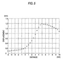
- FIG. 5 is a graph showing the relationship between a relative distance ⁇ X (in FIG. 5, the minus sign indicates a projection) between the side walls of the driving portion 50 and the two side walls 25a and 25b defining the pressure chamber 25, and a displacement Y of the elastic film obtained when the same voltage is applied to the piezoelectric film.
- the displacement of the driving portion 50 is very small and do not largely vary depending on the degree of the projection. This is caused by a phenomenon wherein the piezoelectric film of the driving portion 50 which is outwardly projected from the pressure chamber 25 constrains the side walls 25a and 25b of the pressure chamber 25 of the elastic film.
- the displacement is abruptly increased so that, in the embodiment, it is maximum at a position located on the inner side of the side walls of the pressure chamber 25 by about 5 ⁇ m and gradually reduced in a direction towards the center of the pressure chamber.
- the width of the driving portion 50 is preferably formed so as to be slightly smaller than that of the pressure chamber 24. However, it is not necessary for the width to be smaller in the whole of the length of the pressure chamber. If the driving portion is narrower than only a portion of the pressure chamber, the elastic film is free from the rigidity of the driving portion 50 and hence the degree of displacement can be increased in accordance with the relative distance.
- each of the pressure chambers 25 is provided with the ink supply ports 28 and 29 formed at both the ends in the axial direction. As shown in FIG. 7, therefore, ink flows along paths which are respectively directed as indicated by arrows F from both the ends of the pressure chamber 25 to the center portion where the nozzle opening 52 is formed. Consequently, stagnation of ink at a corner of a pressure chamber which may often occur in a recording head wherein ink is supplied to a pressure chamber through a single ink supply port can be prevented from occurring, and an air bubble in a pressure chamber can be easily discharged to the outside together with an ink drop by the ink flow.
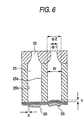
- a metal plate of a thickness of about 90 ⁇ m is usually used as the nozzle plate 53 in the view point of mechanical strength.
- Each nozzle opening 52 formed in the nozzle plate has a smooth conical section shape in which the diameter ⁇ 1 (FIG. 6) on the side of the ink ejection face is about 35 ⁇ m and the diameter ⁇ 2 on the side of the pressure chamber is about 80 ⁇ m.
- the nozzle opening is required to allow ink to smoothly flow and stably eject an ink drop of an amount which is highly accurate.
- the driving portion When the driving portion is configured as a film as described above, a high electric field can be produced by a low voltage. When the film is made thinner, however, stress of a low degree is produced. In order to obtain certain displacement, therefore, the flexural rigidity of the elastic film must be lowered. When ink in the pressure chamber is to be ejected in the form of an ink drop from the nozzle opening, however, the elastic film 41 must have a rigidity which can endure the pressure of the ink. Consequently, the rigidity of the elastic film cannot be reduced unnecessarily.
- the inventor determined that, when the width W of a pressure chamber is set to be 40 to 50 ⁇ m, the degree of displacement is not reduced and ink is surely pressurized, thereby enabling an ink drop to be satisfactorily ejected from the nozzle opening 52.
- the diameter ⁇ 2 of the nozzle opening on the side of the pressure chamber is about 80 ⁇ m. Therefore, partition walls defining the pressure chambers having the width W of 40 to 60 ⁇ m partly close the nozzle opening, thereby producing a problem in that the ink flow directed toward the nozzle opening is impeded.
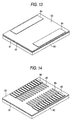
- FIGS. 8a and 8b show an embodiment which can solve the problem.
- 55 designates partition walls defining the pressure chambers 24.
- a nozzle connecting portion 56 is formed by forming recesses 55a so that an opening of a width greater than the diameter ⁇ 2 of the nozzle opening 52 is ensured.
- the nozzle opening is disposed on the other side of the pressure chamber.
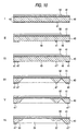
- FIG. 10 shows an embodiment of a method of producing the above-described pressure chamber substrate.
- a single-crystal silicon substrate 40 which is cut at (110) is subjected to thermal oxidation, thereby preparing a base material 42 on which an SiO 2 layer 41 of about 1 ⁇ m is formed on the entire surface.
- the driving portion 50 is formed on the surface of the SiO 2 layer 41 in the same manner as described above with respect to FIG. 4b (Step I).
- a photoresist layer is formed and the SiO 2 layer 41 is removed by using a hydrofluoric acid buffer solution in which hydrofluoric acid and ammonium fluoride are mixed in proportions of 1 : 6, so as to pattern a window 49a for anisotropic etching (Step II).
- the above-mentioned multiple exposure is conducted only on the regions of the SiO 2 layer which will serve as the nozzle connecting portion 56 and in which the ink supply ports 26 are formed.
- Half-etching is then conducted for about 5 min. by using the above-mentioned hydrofluoric acid buffer solution so that the thickness of the SiO 2 layer is reduced to about 0.5 ⁇ m, thereby forming an SiO 2 layer 41' (Step III).
- the base material 42 is immersed into a 10% by weight solution of potassium hydroxide heated to about 80°C, thereby executing anisotropic etching.
- the SiO 2 layers 41 and 41' which have functioned as protective films are gradually dissolved so that a portion of about 0.4 ⁇ m is etched away, with the result that the SiO 2 layer 41' in the regions where the ink supply ports 26, 27, and 28 are to be formed has a thickness of about 0.1 ⁇ m and the SiO 2 layer 41 in the other region has a thickness of about 0.6 ⁇ m (Step IV).
- the base material 42 is immersed into the hydrofluoric acid buffer solution during a period sufficient for removing the SiO 2 layer of 0.1 ⁇ m, for example, about 1 min.
- Step V The base material 42 is immersed into an about 40% by weight solution of potassium hydroxide so as to be subjected to anisotropic etching, whereby the region which opposes the nozzle opening 52 and in which the ink supply port 26 is to be formed are again selectively etched. This makes the regions thinner so that the nozzle connecting portion 56 and the ink supply port 26 having a necessary fluid resistance are formed (Step VI).
- FIGS. 11a and 11b show an embodiment of another recording head which can solve the problems caused by connecting the nozzle opening to the pressure chamber and adjusting the ink amount of an ink drop.
- the reference numeral 60 designates a center partition wall in which one end is fixed to an elastic film 61. The other end of the wall elongates in a region not opposing the nozzle opening 52 to a position abutting the nozzle plate 53, and is configured in the vicinity of the nozzle opening 52 so as to form a through hole 62 which allows ink to pass therethrough.
- one pressure chamber 64 which communicates with the one nozzle opening 52 is divided by the center partition wall 60 into two cells 64a and 64b in communication with each other, and the nozzle plate 53 is supported by a partition wall 65 defining the pressure chamber 64 and by a part of the center partition wall 60.
- the thickness of the center partition wall 60 is selected to be about 15 ⁇ m so that, when the pressure chambers 64 of a length of 2 mm are arranged at a pitch of 141 ⁇ m, the cells 64a and 64b divided by the center partition wall 60 have a width of 46 ⁇ m.
- two driving portions 66 and 67 are formed for each pressure chamber so as to be positioned between the center partition wall 60 and the partition walls 65 defining the pressure chamber 64.
- 68 designates an ink supply port through which an ink reservoir 69 is connected to the pressure chamber 64.
- one pressure chamber 64 can be set to have a width which is approximately equal to the diameter of the nozzle opening 52 on the side of the pressure chamber, whereby the problem of the nozzle opening 52 being closed by the partition wall 65 defining the pressure chamber 64 can be prevented from arising.
- a base material 72 is prepared wherein an SiO 2 layer 71 of a thickness of about 1 ⁇ m is formed by the thermal oxidation method or the like on the entire surface of a single-crystal silicon substrate 70 which is cut so that the surface extends along a (110) crystal axis.
- An elastic film 73 made of zirconia (Zr) or platinum is formed by sputtering on the surface of the base material 72.
- a lower electrode, and a piezoelectric film made of PZT or the like are formed so that two driving portions 74 and 75 are formed for each pressure chamber (Step I).
- a photoresist layer is formed at positions opposing the partition walls 65 and the center partition wall 60 of the pressure chamber.
- the SiO 2 layer 71 is removed by using a hydrofluoric acid buffer solution in which hydrofluoric acid and ammonium fluoride are mixed in proportions of 1 6, so as to pattern a window for anisotropic etching. Thereafter, the above-mentioned multiple exposure is conducted only on an SiO 2 layer 71' of a region where the through hole of the center partition wall 60 is to be formed. Half-etching is then conducted for about 5 min. by using the above-mentioned hydrofluoric acid buffer solution so that the SiO 2 layer 71' of a thickness of about 0.5 ⁇ m is formed (Step II).
- the base material 72 is immersed into a 10% by weight solution of potassium hydroxide heated to about 80°C, thereby executing anisotropic etching.
- the SiO 2 layers 71 and 71' which have functioned as protective films are gradually dissolved so that a portion of about 0.4 ⁇ m is etched away, with the result that the SiO 2 layer 71' in the regions where the through hole of the center partition wall 60 is to be formed has a thickness of about 0.1 ⁇ m and the SiO 2 layer 71 in the other region has a thickness of about 0.6 ⁇ m (Step III).
- the base material 72 is immersed into the hydrofluoric acid buffer solution for, for example, about 1 min. so that the SiO 2 layer 71' in the region where the through hole of the center partition wall 60 is to be formed is removed away and an SiO 2 layer 71" of a thickness of about 0.5 ⁇ m remains in the other region.
- the base material is again immersed into an about 40% weight solution of potassium hydroxide so as to be subjected to anisotropic etching, whereby a step 60a functioning as the through hole 62 is formed in the center partition wall 60 (Step IV).
- the SiO 2 layer 71 in the region of the elastic film 73 opposing the pressure chamber is etched away by using hydrogen fluoride.
- a low-rigidity material such as gold or aluminum is sputtered onto the surfaces of the driving portions 74 and 75 so that an upper electrode 76 is formed (Step V).
- the elastic film 73 is made of a metal such as platinum, the elastic film may function as the lower electrode.
- the driving portions which are formed on the elastic film as described above are configured by using a film forming technique in which a piezoelectric material is sputtered. Therefore, the driving portions are much thinner than those which are formed by applying a green sheet of a piezoelectric material, with the result that the driving portions have a large electrostatic capacity. This produces various problems. Furthermore, since the piezoelectric material existing in the wiring region has piezoelectric properties in the same manner as the driving portions, also the wiring region is displaced, thereby producing a further problem in that the lead pattern formed above is fatigued.
- FIG. 13 shows an embodiment which can solve such problems.
- 80 designates a flow path substrate which is configured by a single-crystal silicon substrate.
- an SiO 2 film 81 and an elastic film 82 which is made of an anticorrosion noble metal or zirconia oxide are formed on the surface of the substrate.
- a lower electrode is formed on the surface of elastic film and a piezoelectric film 83 is then formed so as to cover the entire surface.
- the piezoelectric film 83 is formed by subjecting a material such as a PZT material which conducts flexural vibration in response to an application of an electric field, to a film forming technique, for example, the sputtering method or the sol-gel method.
- the reference numeral 84 designates a low-dielectric constant region having piezoelectric properties and a dielectric constant which are lower than those of the piezoelectric film 83.
- the low-dielectric constant region is formed in a wiring region where a lead pattern for supplying a signal to the driving portion is disposed.
- etching or the like is conducted so that only the regions of the piezoelectric film 83 opposing the pressure chambers remain and the low-dielectric constant region 84 has a shape suitable for the formation of the lead pattern, thereby configuring driving portions 85 and lead pattern forming portions 86.
- a film of platinum which will function as a lower electrode 92 is formed so as to have a thickness of 800 nm on the surface of an etching protective film 91 of a single-crystal silicon substrate 90 by a thin-film formation method such as the sputtering film formation method.
- a thin-film formation method such as the sputtering film formation method.
- a very-thin intermediate layer of titanium or chromium may be formed.
- the lower electrode 92 serves also as an elastic film.
- a film of a first piezoelectric film precursor 93 is formed on the lower electrode.
- the film formation was conducted by the sol-gel method by using a PZT piezoelectric film precursor material in which lead titanate and lead zirconate are mixed at a mole compounding ratio of 55% and 45%, and repeating steps of applying, drying, and degreasing six times so as to obtain a thickness of 1 ⁇ m.
- the lead oxide film 94 other than the region which will function as a wiring region 95 is etched away. Thereafter, the whole of the substrate is heated in an oxygen ambient at 650°C for 3 min. and then at 900°C for 1 min. The substrate is naturally cooled so that the first piezoelectric film precursor 93 is crystallized to be completed as a piezoelectric film 96.
- the lead of the lead oxide film 94 is caused by the above-mentioned heating to be diffused and dissolved into the first piezoelectric film precursor 93, with the result that a different composition film 97 having a low dielectric constant is baked. Analyzation of the different composition film 97 showed that lead was increased to an amount which is 1.12 times the total number of moles of zirconia and titanium (Step II). A film of platinum of a thickness of 200 nm is formed by sputtering on the surfaces of the piezoelectric film 96 and the different composition film 97, thereby forming an upper electrode 98 (step III).
- the upper electrode 97 and the piezoelectric film 95 are divided into a predetermined shape by ion milling using an etching mask so as to correspond to the positions where the pressure chambers are to be formed (Step IV).
- the etching protective film 91 on the opposite face of the single-crystal silicon substrate 90 is removed away by hydrogen fluoride so as to coincide of the shapes of the pressure chamber, a reservoir, and an ink supply port, thereby forming a window 99 (Step V).
- the single-crystal silicon substrate 90 is subjected to anisotropic etching using an anisotropic etchant, for example, an approximately 17% by weight aqueous solution of potassium hydroxide heated to 80°C, so that the etched portion reaches the protective film 91 on the surface. Thereafter, the protective film 91 on the back face of the piezoelectric film 95 is removed by hydrogen fluoride and a flow path of a pressure chamber 100, etc. is formed (Step VI).
- an anisotropic etchant for example, an approximately 17% by weight aqueous solution of potassium hydroxide heated to 80°C
- the thus formed driving portion has an electrostatic capacity of 7 nF per element. As compared with an electrostatic capacity of about 10 nF obtained in the prior art, the electrostatic capacity is reduced by about 30%.
- Reliability evaluation tests by means of long term printing were performed. In prior art recording heads, at 50,000,000 ink drop ejections, a lead pattern was broken or a film separation occurred so that a signal supply was disabled. By contrast, in recording heads according to the invention, the defective rate was reduced or about 1% or less even at 2,000,000,000 ink ejections. This was caused by the fact that the amount of lead in the different composition film 96 in the wiring region is larger than that in the piezoelectric film 95 so that the composition is deviated from the optimum composition of a piezoelectric film.
- the dielectric constants and piezoelectric properties of the piezoelectric film 95 and the different composition film 96 were measured.
- the measurement results show that the piezoelectric film 95 and the different composition film 96 have dielectric constants of 1,800 and 900, respectively, and piezoelectric properties of 150 PC/N and 80 PC/N, respectively. It was confirmed that, according to the invention, both the electrostatic capacity of one element and the piezoelectric displacement of the wiring region are reduced and the mechanical fatigue and the fatigue due to a heat cycle in a lead pattern are decreased.
- the lead oxide film 94 to be formed on the surface of the PZT precursor 93 was baked with various thicknesses for the lead oxide film so that the content of lead oxide with respect to the stoichiometrical composition of the different composition film 96 was varied. It was found that, when a composition is attained in which the amount of lead oxide with respect to the stoichiometrical composition is 0.85 or smaller or 1.10 or larger, piezoelectric properties are largely lowered. Piezoelectric properties were similarly evaluated by using titanium oxide or zirconium oxide in place of lead oxide.
- the elastic film is made of a PZT material. It is obvious that, even when a material to which another metal oxide such as nickel niobate, nickel oxide, or magnesium oxide is added, or a material other than a PZT material is used, the same effects can be attained by adding a material which ensures the adhesion to a substrate and lowers piezoelectric properties and the dielectric constant.
- FIGS. 16 and 17 show a further embodiment in which the displacement and the electrostatic capacity of a piezoelectric film in a wiring region can be reduced.
- a low-dielectric constant layer 111 is formed in a wiring region in the surface of a piezoelectric film 110 which is formed of the entire surface of an elastic plate 82.
- etching or the like is conducted so that only the regions of the piezoelectric film 110 opposing the pressure chambers remain and the low-dielectric constant layer 111 has a shape suitable for the formation of the lead pattern, thereby configuring driving portions 112 and lead pattern forming portions 113.
- a film of platinum which will function as a lower driving electrode 92 is formed so as to have a thickness of 800 nm on the surface of the etching protective film 91 of the single-crystal silicon substrate 90 on the side of a piezoelectric layer, by a thin-film formation method such as a sputtering film formation method.
- a film of a first piezoelectric film precursor 114 is formed on the lower driving electrode 92.
- the film formation was conducted by the sol-gel method by using a PZT-PMN piezoelectric film precursor material in which lead titanate, lead zirconate, and magnesium-lead niobate are mixed at a mole compounding ratio of 55%, 40%, and 10%, and repeating steps of applying, drying, and degreasing six times so as to obtain a thickness of 1 ⁇ m.
- a titanium layer 115 which has a thickness of 50 nm and will function as the low-dielectric constant layer 111 is formed by sputtering on the surface of the precursor 114.
- the titanium layer 115 other than the region which will function as a wiring region 116 is etched away. Thereafter, the whole of the substrate is heated in an oxygen ambient at 650°C for 3 min. and then at 900°C for 1 min. The substrate is naturally cooled so that the precursor 114 is crystallized to be completed as a piezoelectric film.
- the titanium layer 115 becomes as titanium oxide of a thickness of about 100 nm so as to form the low-dielectric constant layer (Step II).
- a film of platinum of a thickness of 200 nm is formed by sputtering on the surfaces of the piezoelectric film 117 and the titanium oxide film 118, thereby forming an upper electrode 119 (Step III).
- the upper electrode 119 and the piezoelectric film 117 are divided into a predetermined shape by ion milling so as to correspond to the positions where the pressure chambers are to be formed (Step IV).
- the etching protective film 91 on the opposite face of the substrate 90 is etched away by hydrogen fluoride so as to coincide of the shapes of the pressure chamber, a reservoir, and an ink supply port, thereby forming the window 99 (Step V).
- the single-crystal silicon substrate 90 is subjected to anisotzopic etching with using an anisotropic etchant, for example, an about 17% by weight aqueous solution of potassium hydroxide heated to 80°C, so that the etched portion reaches the protective film 91 on the surface.
- an anisotropic etchant for example, an about 17% by weight aqueous solution of potassium hydroxide heated to 80°C, so that the etched portion reaches the protective film 91 on the surface.
- the thus formed driving portion has an electrostatic capacity of 5 nF per element. As compared with an electrostatic capacity of about 10 nF obtained in the prior art, the electrostatic capacity is reduced to about one half. Reliability evaluation tests by means of long term printing were performed. In prior art recording heads, at 50,000,000 ink drop ejections, an ink ejection failure occurred in 10% of the recording heads. By contrast, in recording heads according to the invention, the defective rate was about 1% or less even at 2,000,000,000 ink ejections.
- the layer may be made of a material which is suitable for forming a low-dielectric constant film, such as silicon, silicon oxide, aluminum oxide, zirconium oxide or lead oxide. It is preferable to use a material which contains an element which configures the piezoelectric film 117, in order to enhance the adhesion strength exerted between films and prevent an unexpected reaction from occurring.
- the low-dielectric constant layer and the piezoelectric film are simultaneously baked. Alternatively, they may be separately baked, or formed without conducting the baking process or by depositing a low-dielectric constant material on the surface of a piezoelectric film.
- the low-dielectric constant layer 111 is made of a material which is lower in dielectric constant than the piezoelectric film.
- the layer may be made of the same material as the piezoelectric film, the upper electrode 119 may be formed by sputtering platinum in the same manner as described above, and the upper electrode and the lead portion may be then patterned.
- the lead portion can be thicker than the region which functions as the piezoelectric member, and hence it is apparent that the electrostatic capacity of the wiring region can be reduced.
- the wiring region is formed by the same piezoelectric material as described above, it is preferable in the view point of production to employ a configuration in which a piezoelectric material layer of a uniform thickness suitable for a wiring region and the region other than the wiring region is caused by etching or the like to function as the piezoelectric film.
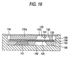
- a pressure chamber 130 is formed in the form of a through hole on a flow path substrate 133 in which the pressure chamber 130, an ink supply port 131, and a reservoir 132 are formed.
- a nozzle plate 134 is liquid-tightly fixed to one face of the substrate.
- a pressure film substrate 136 on which a driving portion 135 is formed and which is configured as a separate member is liquid-tightly fixed to the other face of the substrate.
- an elastic film 138 functioning also as a lower electrode, a piezoelectric film 139, and an upper electrode 140 are formed on the surface of a single-crystal silicon substrate by the same technique described above, and then patterned so as to be formed as the driving portion 135. Thereafter, anisotropic etching is conducted on the opposite face (in the figure, the lower face) of the single-crystal silicon substrate and a recess 142 is formed so that a wall 141 is positioned between the driving portions 135.
- the elastic film 138 can be supported at various points by the wall 141, and hence crosstalk can be prevented from occurring even when a partition wall 130a defining the pressure chamber 130 of the flow path substrate 133 is made thin so that the arrangement pitch of the pressure chambers 130 is small. Since the elastic film 138 having the driving portions 135 can be formed as a separate member, the pressure chamber can be configured by conducting etching on the face of the flow path substrate 133 opposite to the side where a nozzle opening 143 is opened, i.e., the face opposite to that used in the case where an elastic film is integrated with a flow path substrate.
- the pressure chamber 131 can be formed into a shape in which the dimension is gradually reduced in a direction moving from the driving portion 135 toward the nozzle opening 143, so that ink pressurized in the pressure chamber 130 is allowed to smoothly flow to the nozzle opening 143.
Landscapes
- Engineering & Computer Science (AREA)
- Manufacturing & Machinery (AREA)
- Particle Formation And Scattering Control In Inkjet Printers (AREA)
Claims (24)
- Tête d'enregistrement à jets d'encre, comprenant :dans laquelle les chambres de pression (3, 4 ; 24, 25 ; 64 ; 100 ; 130) sont disposées dans un substrat de silicium monocristallin (40 ; 70 ; 90) ayant un plan de réseau (110),une plaque à buses (12 ; 53 ; 134) dans laquelle sont formées plusieurs ouvertures de buse (10, 11 ; 52 ; 143),un substrat à trajets de circulation qui comprend un réservoir (5, 6 ; 21, 22, 23 ; 69 ; 132) auquel de l'encre est transmise depuis l'extérieur, et plusieurs chambres de pression (3, 4 ; 24, 25 ; 64 ; 100 ; 130) qui sont raccordées au réservoir (5, 6 ; 21, 22, 23 ; 69 ; 132) par un canal de transmission d'encre (26, 27, 28, 29 ; 68 ; 131) et qui communiquent respectivement avec les ouvertures de buse (10, 11 ; 52 ; 143),un film élastique (43 ; 61 ; 73 ; 82 ; 138) qui met sous pression l'encre contenue dans les chambres de pression (3, 4 ; 24, 25 ; 64 ; 100 ; 130), et un dispositif de pilotage placé en position opposée à la chambre respective de pression (3, 4 ; 24, 25 ; 64 ; 100 ; 130) afin que le film élastique (43 ; 61 ; 73 ; 82 ; 138) effectue une déformation de flexion,
caractérisée en ce que
les chambres de pression (3, 4 ; 24, 25 ; 64 ; 100 ; 130) sont disposées dans une rangée qui s'étend avec une orientation de réseau <112> ou une orientation de réseau équivalant à l'orientation de réseau <112>. - Tête d'enregistrement à jets d'encre selon la revendication 1, dans laquelle le film élastique (43 ; 61 ; 73 ; 82 ; 138) est formé en une seule pièce avec une première face du substrat de silicium monocristallin (40 ; 70 ; 90) par un procédé de formation de film, et/ou le dispositif de pilotage est formé par un élément piézoélectrique dans une structure stratifiée et solidaire du substrat de silicium monocristallin (40 ; 70 ; 90) et/ou l'élément piézoélectrique comporte un premier film d'électrode formé sur une surface du film élastique (43 ; 61 ; 73 ; 82 ; 138), un film piézoélectrique (13, 14 ; 44 ; 83 ; 96 ; 110 ; 117 ; 139) formé sur le premier film d'électrode, et un second film d'électrode formé sur le film piézoélectrique (13, 14 ; 44 ; 83 ; 96 ; 110 ; 117 ; 139).
- Tête d'enregistrement à jets d'encre selon la revendication 1 ou 2, dans laquelle une partie au moins du dispositif de pilotage a une région plus étroite que la largeur de la chambre de pression (3, 4 ; 24, 25 ; 64 ; 100 ; 130).
- Tête d'enregistrement à jets d'encre selon l'une des revendications 1 à 3, dans laquelle une partie au moins du dispositif de pilotage a une région plus étroite que la largeur de la chambre de pression (3, 4 ; 24, 25 ; 64 ; 100 ; 130).
- Tête d'enregistrement à jets d'encre selon l'une des revendications 2 à 4, dans laquelle le premier film d'électrode est utilisé comme film élastique (43 ; 61 ; 73 ; 82 ; 138) et a une épaisseur de 0,2 à 2,5 µm.
- Tête d'enregistrement à jets d'encre selon l'une des revendications précédentes, dans laquelle le canal de transmission d'encre (26, 27, 28, 29 ; 68 ; 131) est formé aux deux extrémités dans la direction longitudinale de la chambre de pression (3, 4 ; 24, 25 ; 64 ; 100 ; 130).
- Tête d'enregistrement à jets d'encre selon l'une des revendications 1 à 6, dans laquelle une partie de raccordement de buse (56) est formée dans une première région des chambres de pression (24, 25), la partie de raccordement de buse (56) étant opposée aux ouvertures de buse (52), et la partie de raccordement de buse (56) étant plus large qu'une seconde région des chambres de pression (24, 25).
- Tête d'enregistrement à jets d'encre selon la revendication 7, dans laquelle la partie de raccordement de buse (56) est formée à une position opposée à une face inclinée à une partie d'extrémité de la chambre de pression (24, 25).
- Tête d'enregistrement à jets d'encre selon l'une des revendications 1 à 8, dans laquelle la chambre de pression (24, 25 ; 64) est divisée, par une paroi centrale de cloison (60) qui s'allonge depuis le film élastique (43), en plusieurs cellules (64a, 64b) qui communiquent mutuellement au moins au voisinage de l'ouverture de buse (52), la chambre de pression (24, 25 ; 64) communiquant avec une ouverture de buse (52), et une partie de la paroi centrale de cloison (60) supporte la plaque à buses (53).
- Tête d'enregistrement à jets d'encre selon l'une des revendications 1 à 9, comprenant en outre, sur une surface du film élastique (73 ; 82), une électrode inférieure (92), et un film piézoélectrique (96) formé dans une région opposée à la chambre respective de pression (24, 25 ; 64 ; 100), et un film d'une composition différente (97) formé dans une région de câblage (95) pour la transmission d'un signal de pilotage au film piézoélectrique (96), le film de composition différente (97) ayant une constante diélectrique et des propriétés piézoélectriques qui sont inférieures à celles du film piézoélectrique (96), une électrode supérieure (98) formée à une surface du film piézoélectrique (96), et un motif de fils de connexion formé à une surface du film de composition différente (97) et connecté à l'électrode supérieure (98).
- Tête d'enregistrement à jets d'encre selon la revendication 10, dans laquelle le film piézoélectrique (96) et le film de composition différente (97) contiennent un élément identique et ont des compositions différentes.
- Tête d'enregistrement à jets d'encre selon la revendication 10 ou 11, dans laquelle le film piézoélectrique (96) est formé de PbCTiAZrBO3 (A, B et C étant des nombres tels que A + B = 1, 0,5 ≤ A ≤ 0,6, et 0,85 ≤ C ≤ 1,10).
- Tête d'enregistrement à jets d'encre selon l'une des revendications 10 à 12, dans laquelle le film de composition différente (97) est formé de PbCTiAZrBO3 (A, B et C étant des nombres tels que A + B = 1 et A < 0,5 ou 0,6 < A).
- Tête d'enregistrement à jets d'encre selon l'une des revendications 10 à 12, dans laquelle le film de composition différente (97) est formé de PbCTiAZrBO3 (A, B et C étant des nombres tels que A + B = 1 et C < 0,85 ou 1,10 < C) .
- Tête d'enregistrement à jets d'encre selon l'une des revendications 10 à 14, dans laquelle le film piézoélectrique (96) contient Pb(Mg1/3Nb2/3O3).
- Tête d'enregistrement à jets d'encre selon l'une des revendications 10 à 15, dans laquelle la région de câblage (95) est formée dans une région qui n'est pas opposée au réservoir (21, 22, 23).
- Tête d'enregistrement à jets d'encre selon l'une des revendications 1 à 16, dans laquelle une électrode inférieure (92) et un film piézoélectrique (96) sont stratifiés sur une surface du film élastique (82), et un film de faible constante diélectrique (111) qui est inférieure à la constante diélectrique du film piézoélectrique (96) et une électrode supérieure (98) sont stratifiés dans une région de câblage (95) pour la transmission d'un signal de pilotage au film piézoélectrique (96).
- Tête d'enregistrement à jets d'encre selon la revendication 17, dans laquelle le film de faible constante diélectrique (111) est formé d'un oxyde d'un élément métallique qui donne sa configuration au film piézoélectrique (96).
- Tête d'enregistrement à jets d'encre selon la revendication 17 ou 18, dans laquelle le film piézoélectrique (96) est formé de PbTiAZrB(Mg1/3Nb2/3)CO3 + ePbO (A, B, C et e étant des nombres tels que A + B + C = 1, 0,35 ≤ A ≤ 0,55, 0,25 ≤ B ≤ 0,55, 0,1 ≤ C ≤ 0,4 et 0 ≤ e ≤ 0,3).
- Tête d'enregistrement à jets d'encre selon l'une des revendications 17 à 19, dans laquelle le film de faible constante diélectrique (111) est formé d'au moins un composé choisi dans le groupe constitué par l'oxyde de plomb, l'oxyde de titane et l'oxyde de zirconium.
- Tête d'enregistrement à jets d'encre selon l'une des revendications 1 à 20, dans laquelle une électrode inférieure (92), un film piézoélectrique (96), une région de câblage (95) dans laquelle est placé un matériau piézoélectrique ayant une composition identique à la composition du film piézoélectrique (96), et une électrode supérieure (98) formant des motifs par attaque chimique sont stratifiés sur une surface du film élastique (73 ; 82).
- Tête d'enregistrement à jets d'encre, comprenant :dans laquelle le substrat est un substrat de silicium monocristallin taillé suivant un plan de réseau (110),une plaque à buses (12 ; 53 ; 134) ayant plusieurs ouvertures de buse (10, 11 ; 52 ; 143),un substrat à trajets de circulation dans lequel sont disposées plusieurs chambres de pression (3, 4 ; 24, 25 ; 64 ; 100 ; 130) qui communiquent avec les ouvertures de buse formées dans la plaque à buses,un film élastique (43 ; 61 ; 73 ; 82 ; 138) formé sur une face du substrat opposée aux chambres de pression, etun dispositif destiné à faire fléchir le film élastique afin que l'encre présente dans les chambres de pression soit mise sous pression,
caractérisé en ce que
les chambres de pression sont disposées dans une rangée qui s'étend avec une orientation de réseau <112> ou une orientation de réseau équivalant à l'orientation de réseau <112>. - Procédé de production d'une tête d'enregistrement à jets d'encre, comprenant :caractérisé en ce queune étape de formation d'un film de protection contre une attaque sur un substrat de silicium monocristallin dans lequel le plan de réseau d'une surface est (110),une première étape de mise sous forme de motifs comprenant l'enlèvement d'une partie du film de protection contre l'attaque sur une face du substrat de silicium monocristallin, avec formation de cette manière de plusieurs fenêtres correspondant chacune à une chambre de pression,une seconde étape de formation de motifs comprenant l'amincissement du film de protection contre l'attaque dans une région opposée à une partie de raccordement de buse et un canal de transmission d'encre,une première étape d'attaque destinée à effectuer une attaque anisotrope sur le substrat de silicium monocristallin avec la fenêtre formée dans la première étape de formation de motifs,une seconde étape d'attaque destinée à retirer le film de protection contre l'attaque qui est aminci dans la seconde étape de mise sous forme de motifs, etl'exécution d'une attaque anisotrope,
les chambres de pression sont disposées suivant une ligne qui s'étend avec l'orientation de réseau <112> ou une orientation de réseau équivalant à l'orientation de réseau <112>. - Procédé selon la revendication 23, dans lequel l'étape d'attaque anisotrope forme un gradin au centre d'une paroi de cloison.
Priority Applications (1)
| Application Number | Priority Date | Filing Date | Title |
|---|---|---|---|
| EP99121357A EP0974466B1 (fr) | 1995-04-19 | 1996-04-19 | Tête d'enregistrement à jet d'encre et procédé de sa production |
Applications Claiming Priority (15)
| Application Number | Priority Date | Filing Date | Title |
|---|---|---|---|
| JP94017/95 | 1995-04-19 | ||
| JP9401995A JPH08281945A (ja) | 1995-04-19 | 1995-04-19 | インクジェットヘッド及びインクジェットヘッドの製造方法 |
| JP9401995 | 1995-04-19 | ||
| JP9401795A JP3384184B2 (ja) | 1995-04-19 | 1995-04-19 | インクジェットプリントヘッド |
| JP94019/95 | 1995-04-19 | ||
| JP9401795 | 1995-04-19 | ||
| JP32085895A JP3407514B2 (ja) | 1995-12-08 | 1995-12-08 | 液体吐出装置 |
| JP32085895 | 1995-12-08 | ||
| JP320858/95 | 1995-12-08 | ||
| JP32265695 | 1995-12-12 | ||
| JP32265795 | 1995-12-12 | ||
| JP32265795A JPH09156099A (ja) | 1995-12-12 | 1995-12-12 | インクジェットプリントヘッド及びその製造方法 |
| JP32265695A JPH09156098A (ja) | 1995-12-12 | 1995-12-12 | インクジェットプリントヘッド及びその製造方法 |
| JP322656/95 | 1995-12-12 | ||
| JP322657/95 | 1995-12-12 |
Related Child Applications (1)
| Application Number | Title | Priority Date | Filing Date |
|---|---|---|---|
| EP99121357A Division EP0974466B1 (fr) | 1995-04-19 | 1996-04-19 | Tête d'enregistrement à jet d'encre et procédé de sa production |
Publications (3)
| Publication Number | Publication Date |
|---|---|
| EP0738599A2 EP0738599A2 (fr) | 1996-10-23 |
| EP0738599A3 EP0738599A3 (fr) | 1997-09-10 |
| EP0738599B1 true EP0738599B1 (fr) | 2002-10-16 |
Family
ID=27525672
Family Applications (2)
| Application Number | Title | Priority Date | Filing Date |
|---|---|---|---|
| EP99121357A Expired - Lifetime EP0974466B1 (fr) | 1995-04-19 | 1996-04-19 | Tête d'enregistrement à jet d'encre et procédé de sa production |
| EP96106204A Expired - Lifetime EP0738599B1 (fr) | 1995-04-19 | 1996-04-19 | Tête d'enregistrement à jet d'encre et procédé pour sa fabrication |
Family Applications Before (1)
| Application Number | Title | Priority Date | Filing Date |
|---|---|---|---|
| EP99121357A Expired - Lifetime EP0974466B1 (fr) | 1995-04-19 | 1996-04-19 | Tête d'enregistrement à jet d'encre et procédé de sa production |
Country Status (3)
| Country | Link |
|---|---|
| US (2) | US5754205A (fr) |
| EP (2) | EP0974466B1 (fr) |
| DE (2) | DE69624282T2 (fr) |
Families Citing this family (80)
| Publication number | Priority date | Publication date | Assignee | Title |
|---|---|---|---|---|
| JP3379106B2 (ja) * | 1992-04-23 | 2003-02-17 | セイコーエプソン株式会社 | 液体噴射ヘッド |
| JP3386099B2 (ja) * | 1995-07-03 | 2003-03-10 | セイコーエプソン株式会社 | インクジェット式記録ヘッド用ノズルプレート、これの製造方法、及びインクジェット式記録ヘッド |
| US6729002B1 (en) | 1995-09-05 | 2004-05-04 | Seiko Epson Corporation | Method of producing an ink jet recording head |
| DE69629220T2 (de) | 1995-09-05 | 2004-04-15 | Seiko Epson Corp. | Tintenstrahlaufzeichunugskopf und sein Herstellungsverfahren |
| JP3460218B2 (ja) * | 1995-11-24 | 2003-10-27 | セイコーエプソン株式会社 | インクジェットプリンタヘッドおよびその製造方法 |
| US7003857B1 (en) | 1995-11-24 | 2006-02-28 | Seiko Epson Corporation | Method of producing an ink-jet printing head |
| JP3503386B2 (ja) * | 1996-01-26 | 2004-03-02 | セイコーエプソン株式会社 | インクジェット式記録ヘッド及びその製造方法 |
| US6305791B1 (en) * | 1996-07-31 | 2001-10-23 | Minolta Co., Ltd. | Ink-jet recording device |
| US6290341B1 (en) | 1996-10-18 | 2001-09-18 | Seiko Epson Corporation | Ink jet printing head which prevents the stagnation of ink in the vicinity of the nozzle orifices |
| JP3713921B2 (ja) | 1996-10-24 | 2005-11-09 | セイコーエプソン株式会社 | インクジェット式記録ヘッドの製造方法 |
| JP2861980B2 (ja) * | 1997-01-30 | 1999-02-24 | 日本電気株式会社 | インク滴噴射装置 |
| JPH10305578A (ja) * | 1997-03-03 | 1998-11-17 | Seiko Epson Corp | インクジェット式記録ヘッド |
| JPH10264374A (ja) * | 1997-03-27 | 1998-10-06 | Seiko Epson Corp | インクジェット式記録ヘッド |
| US6231169B1 (en) | 1997-04-30 | 2001-05-15 | Seiko Epson Corporation | Ink jet printing head including a backing member for reducing displacement of partitions between pressure generating chambers |
| DE69810835T2 (de) | 1997-04-30 | 2003-08-07 | Seiko Epson Corp., Tokio/Tokyo | Tintenstrahlaufzeichnungskopf |
| US6254793B1 (en) * | 1997-07-15 | 2001-07-03 | Silverbrook Research Pty Ltd | Method of manufacture of high Young's modulus thermoelastic inkjet printer |
| US6460971B2 (en) | 1997-07-15 | 2002-10-08 | Silverbrook Research Pty Ltd | Ink jet with high young's modulus actuator |
| JPH1191102A (ja) * | 1997-09-25 | 1999-04-06 | Nec Corp | 固体アクチュエータおよびインクジェットヘッド |
| JP3521708B2 (ja) * | 1997-09-30 | 2004-04-19 | セイコーエプソン株式会社 | インクジェット式記録ヘッドおよびその製造方法 |
| US6322203B1 (en) * | 1998-02-19 | 2001-11-27 | Seiko Epson Corporation | Ink jet recording head and ink jet recorder |
| CA2267921A1 (fr) * | 1998-04-02 | 1999-10-02 | Nec Corporation | Tete d'impression a jet d'encre, sa methode de propulsion d'encre et imprimante les employant |
| JP2940544B1 (ja) * | 1998-04-17 | 1999-08-25 | 日本電気株式会社 | インクジェット記録ヘッド |
| JP2000033713A (ja) | 1998-07-17 | 2000-02-02 | Seiko Epson Corp | インクジェット印刷ヘッド及びインクジェットプリンタ |
| JP3422364B2 (ja) * | 1998-08-21 | 2003-06-30 | セイコーエプソン株式会社 | インクジェット式記録ヘッド及びインクジェット式記録装置 |
| US6616270B1 (en) | 1998-08-21 | 2003-09-09 | Seiko Epson Corporation | Ink jet recording head and ink jet recording apparatus comprising the same |
| WO2000044054A1 (fr) * | 1999-01-22 | 2000-07-27 | Kansai Research Institute | Dispositif a film mince piezoelectrique, procede de production associe et tete d'enregistrement a jet d'encre |
| DE60016478T2 (de) * | 1999-02-18 | 2005-11-10 | Seiko Epson Corp. | Herstellungsverfahren für einen Tintenstrahlaufzeichnungskopf |
| JP3868143B2 (ja) | 1999-04-06 | 2007-01-17 | 松下電器産業株式会社 | 圧電体薄膜素子及びこれを用いたインクジェット式記録ヘッド並びにこれらの製造方法 |
| US6617098B1 (en) * | 1999-07-13 | 2003-09-09 | Input/Output, Inc. | Merged-mask micro-machining process |
| DE60045067D1 (de) * | 1999-08-04 | 2010-11-18 | Seiko Epson Corp | Tintenstrahlaufzeichnungskopf, verfahren zur herstellung und vorrichtung zum tintenstrahlaufzeichnen |
| US6312110B1 (en) | 1999-09-28 | 2001-11-06 | Brother International Corporation | Methods and apparatus for electrohydrodynamic ejection |
| JP3389987B2 (ja) * | 1999-11-11 | 2003-03-24 | セイコーエプソン株式会社 | インクジェット式記録ヘッド及びその製造方法 |
| US6774541B1 (en) * | 1999-11-18 | 2004-08-10 | Kri, Inc. | Piezoelectric element, process for producing the piezoelectric element, and head for ink-jet printer using the piezoelectric element |
| US6958125B2 (en) * | 1999-12-24 | 2005-10-25 | Canon Kabushiki Kaisha | Method for manufacturing liquid jet recording head |
| WO2001074591A1 (fr) * | 2000-03-31 | 2001-10-11 | Fujitsu Limited | Tete a jet d'encre a buses multiples |
| US6526658B1 (en) * | 2000-05-23 | 2003-03-04 | Silverbrook Research Pty Ltd | Method of manufacture of an ink jet printhead having a moving nozzle with an externally arranged actuator |
| JP4380962B2 (ja) * | 2000-05-24 | 2009-12-09 | シルバーブルック リサーチ ピーティワイ リミテッド | インクジェットプリントヘッドの製造方法 |
| US6409311B1 (en) | 2000-11-24 | 2002-06-25 | Xerox Corporation | Bi-directional fluid ejection systems and methods |
| US6419335B1 (en) | 2000-11-24 | 2002-07-16 | Xerox Corporation | Electronic drive systems and methods |
| US6350015B1 (en) | 2000-11-24 | 2002-02-26 | Xerox Corporation | Magnetic drive systems and methods for a micromachined fluid ejector |
| US6416169B1 (en) | 2000-11-24 | 2002-07-09 | Xerox Corporation | Micromachined fluid ejector systems and methods having improved response characteristics |
| US6367915B1 (en) | 2000-11-28 | 2002-04-09 | Xerox Corporation | Micromachined fluid ejector systems and methods |
| US6472332B1 (en) | 2000-11-28 | 2002-10-29 | Xerox Corporation | Surface micromachined structure fabrication methods for a fluid ejection device |
| US6783588B2 (en) * | 2000-12-15 | 2004-08-31 | Canon Kabushiki Kaisha | BaTiO3-PbTiO3 series single crystal and method of manufacturing the same piezoelectric type actuator and liquid discharge head using such piezoelectric type actuator |
| US6406130B1 (en) | 2001-02-20 | 2002-06-18 | Xerox Corporation | Fluid ejection systems and methods with secondary dielectric fluid |
| US6629756B2 (en) | 2001-02-20 | 2003-10-07 | Lexmark International, Inc. | Ink jet printheads and methods therefor |
| JP3603828B2 (ja) * | 2001-05-28 | 2004-12-22 | 富士ゼロックス株式会社 | インクジェット式記録ヘッド及びその製造方法並びにインクジェット式記録装置 |
| JP2003022892A (ja) | 2001-07-06 | 2003-01-24 | Semiconductor Energy Lab Co Ltd | 発光装置の製造方法 |
| US6953241B2 (en) | 2001-11-30 | 2005-10-11 | Brother Kogyo Kabushiki Kaisha | Ink-jet head having passage unit and actuator units attached to the passage unit, and ink-jet printer having the ink-jet head |
| US6979077B2 (en) * | 2002-02-20 | 2005-12-27 | Brother Kogyo Kabushiki Kaisha | Ink-jet head and ink-jet printer having ink-jet head |
| TWI221322B (en) * | 2002-02-26 | 2004-09-21 | Benq Corp | Manufacturing method of fluid spraying apparatus |
| US6520624B1 (en) * | 2002-06-18 | 2003-02-18 | Hewlett-Packard Company | Substrate with fluid passage supports |
| JP4209144B2 (ja) * | 2002-06-21 | 2009-01-14 | パナソニック株式会社 | 圧電アクチュエータ、インクジェットヘッド及びインクジェット式記録装置 |
| US7381341B2 (en) * | 2002-07-04 | 2008-06-03 | Seiko Epson Corporation | Method of manufacturing liquid jet head |
| US20040134881A1 (en) * | 2002-07-04 | 2004-07-15 | Seiko Epson Corporation | Method of manufacturing liquid jet head |
| US7063407B2 (en) * | 2002-08-21 | 2006-06-20 | Matsushita Electric Industrial Co., Ltd. | Piezoelectric actuator, method for manufacturing the same, ink jet head, and ink jet recording apparatus |
| JP3729190B2 (ja) * | 2002-08-23 | 2005-12-21 | セイコーエプソン株式会社 | 液体噴射ヘッドおよびその製造方法 |
| TWI222408B (en) * | 2002-12-03 | 2004-10-21 | Nanodynamics Inc | Pressure chamber of a piezoelectric ink jet print head and fabrication method thereof |
| US7419252B2 (en) * | 2004-07-13 | 2008-09-02 | Brother Kogyo Kabushiki Kaisha | Ink jet head, piezo-electric actuator, and method of manufacturing them |
| JP4595418B2 (ja) * | 2004-07-16 | 2010-12-08 | ブラザー工業株式会社 | インクジェットヘッド |
| US7549223B2 (en) * | 2004-09-28 | 2009-06-23 | Fujifilm Corporation | Method for manufacturing a liquid ejection head |
| US7283030B2 (en) * | 2004-11-22 | 2007-10-16 | Eastman Kodak Company | Doubly-anchored thermal actuator having varying flexural rigidity |
| US7175258B2 (en) * | 2004-11-22 | 2007-02-13 | Eastman Kodak Company | Doubly-anchored thermal actuator having varying flexural rigidity |
| US7188931B2 (en) | 2004-11-22 | 2007-03-13 | Eastman Kodak Company | Doubly-anchored thermal actuator having varying flexural rigidity |
| JP4096318B2 (ja) * | 2005-03-15 | 2008-06-04 | 富士フイルム株式会社 | 液体吐出ヘッド及びその製造方法 |
| EP1705012B1 (fr) * | 2005-03-22 | 2010-11-17 | Brother Kogyo Kabushiki Kaisha | Actuateur piézo-électrique, dispositif de transport de liquide et méthode de production d'actuateur piézo-électrique |
| US7998362B2 (en) * | 2005-08-23 | 2011-08-16 | Canon Kabushiki Kaisha | Piezoelectric substance, piezoelectric element, liquid discharge head using piezoelectric element, liquid discharge apparatus, and production method of piezoelectric element |
| JP2008049531A (ja) * | 2006-08-23 | 2008-03-06 | Canon Inc | インクジェット記録ヘッド |
| JP5103951B2 (ja) * | 2007-03-08 | 2012-12-19 | ブラザー工業株式会社 | 駆動装置及び液滴吐出ヘッド |
| US8313174B2 (en) | 2008-08-06 | 2012-11-20 | Xerox Corporation | Method for reducing mechanical cross-talk between array structures on a substrate mounted to another substrate by an adhesive |
| US8287094B2 (en) | 2009-07-27 | 2012-10-16 | Zamtec Limited | Printhead integrated circuit configured for backside electrical connection |
| US8323993B2 (en) * | 2009-07-27 | 2012-12-04 | Zamtec Limited | Method of fabricating inkjet printhead assembly having backside electrical connections |
| CN102972046B (zh) * | 2010-06-30 | 2016-08-03 | 日本电气株式会社 | 振荡装置和电子设备 |
| US8864287B2 (en) * | 2011-04-19 | 2014-10-21 | Eastman Kodak Company | Fluid ejection using MEMS composite transducer |
| US9590587B1 (en) | 2011-07-07 | 2017-03-07 | Analog Devices, Inc. | Compensation of second order temperature dependence of mechanical resonator frequency |
| US9214623B1 (en) | 2012-01-18 | 2015-12-15 | Analog Devices, Inc. | Doped piezoelectric resonator |
| JP6061088B2 (ja) * | 2013-03-28 | 2017-01-18 | セイコーエプソン株式会社 | 液体噴射ヘッド及び液体噴射装置 |
| JP6314519B2 (ja) * | 2014-02-10 | 2018-04-25 | セイコーエプソン株式会社 | 導通構造、導通構造の製造方法、液滴吐出ヘッドおよび印刷装置 |
| JP6609943B2 (ja) * | 2015-03-12 | 2019-11-27 | セイコーエプソン株式会社 | タンク、タンクユニットおよび液体噴射システム |
| JP7214468B2 (ja) * | 2018-12-25 | 2023-01-30 | キヤノン株式会社 | 液体吐出ヘッド |
Family Cites Families (13)
| Publication number | Priority date | Publication date | Assignee | Title |
|---|---|---|---|---|
| JPS5511811A (en) * | 1978-07-10 | 1980-01-28 | Seiko Epson Corp | Liquid jet device |
| US4516140A (en) * | 1983-12-27 | 1985-05-07 | At&T Teletype Corporation | Print head actuator for an ink jet printer |
| DE3917434A1 (de) * | 1989-05-29 | 1989-11-09 | Siemens Ag | Mehrschichtig aufgebauter tintendruckkopf mit durch selektives aetzen erzeugten tintenkanaelen |
| EP0408306B1 (fr) * | 1989-07-11 | 1996-05-01 | Ngk Insulators, Ltd. | Organe d'actionnement piézo-électrique/électrostrictif comportant au moins une couche piézoélectrique/électrostrictive |
| US5534900A (en) * | 1990-09-21 | 1996-07-09 | Seiko Epson Corporation | Ink-jet recording apparatus |
| US5265315A (en) * | 1990-11-20 | 1993-11-30 | Spectra, Inc. | Method of making a thin-film transducer ink jet head |
| JPH05177831A (ja) * | 1991-12-27 | 1993-07-20 | Rohm Co Ltd | インクジェットプリントヘッド及びそれを備える電子機器 |
| JP3147132B2 (ja) * | 1992-03-03 | 2001-03-19 | セイコーエプソン株式会社 | インクジェット記録ヘッド、インクジェット記録ヘッド用振動板、及びインクジェット記録ヘッド用振動板の製造方法 |
| JP3379106B2 (ja) * | 1992-04-23 | 2003-02-17 | セイコーエプソン株式会社 | 液体噴射ヘッド |
| JP3168713B2 (ja) * | 1992-08-06 | 2001-05-21 | セイコーエプソン株式会社 | インクジェットヘッド及びその製造方法 |
| US5896150A (en) * | 1992-11-25 | 1999-04-20 | Seiko Epson Corporation | Ink-jet type recording head |
| JP3235630B2 (ja) * | 1993-11-05 | 2001-12-04 | セイコーエプソン株式会社 | インクジェット式記録ヘッド |
| JP3109703B2 (ja) * | 1993-12-21 | 2000-11-20 | キヤノン株式会社 | メンブレン構造体及びその製造方法及びそれを用いたマイクロデバイス |
-
1996
- 1996-04-19 EP EP99121357A patent/EP0974466B1/fr not_active Expired - Lifetime
- 1996-04-19 DE DE69624282T patent/DE69624282T2/de not_active Expired - Fee Related
- 1996-04-19 US US08/634,770 patent/US5754205A/en not_active Expired - Lifetime
- 1996-04-19 EP EP96106204A patent/EP0738599B1/fr not_active Expired - Lifetime
- 1996-04-19 DE DE69627045T patent/DE69627045T2/de not_active Expired - Fee Related
-
1997
- 1997-02-06 US US08/795,565 patent/US5922218A/en not_active Expired - Lifetime
Also Published As
| Publication number | Publication date |
|---|---|
| DE69624282T2 (de) | 2003-07-03 |
| US5754205A (en) | 1998-05-19 |
| DE69627045T2 (de) | 2003-09-25 |
| EP0974466A1 (fr) | 2000-01-26 |
| DE69627045D1 (de) | 2003-04-30 |
| EP0738599A3 (fr) | 1997-09-10 |
| EP0738599A2 (fr) | 1996-10-23 |
| US5922218A (en) | 1999-07-13 |
| EP0974466B1 (fr) | 2003-03-26 |
| DE69624282D1 (de) | 2002-11-21 |
Similar Documents
| Publication | Publication Date | Title |
|---|---|---|
| EP0738599B1 (fr) | Tête d'enregistrement à jet d'encre et procédé pour sa fabrication | |
| EP0786346B1 (fr) | Tête d'enregistrement à jet d'encre | |
| EP1101615B1 (fr) | Tête et dispositif d'enregistrement à jet d'encre | |
| EP2451647B1 (fr) | Structure d'éjection à système microélectromécanique, pour agencement dense | |
| KR101153562B1 (ko) | 압전 방식의 잉크젯 프린트헤드 및 그 제조방법 | |
| US6712456B2 (en) | Ink-jet recording head, manufacturing method of the same and ink-jet recording apparatus | |
| EP1693206A1 (fr) | Tête d'impression jet d'encre piezoélectrique et sa méthode de fabrication | |
| KR100498851B1 (ko) | 잉크젯 기록 헤드 및 잉크젯 기록 장치 | |
| EP0893259B1 (fr) | Tête d'impression à jet d'encre et son procédé de fabrication | |
| US6364468B1 (en) | Ink-jet head and method of manufacturing the same | |
| US20030117464A1 (en) | Liquid-jet head and liquid-jet apparatus | |
| US6371598B1 (en) | Ink jet recording apparatus, and an ink jet head | |
| US6231169B1 (en) | Ink jet printing head including a backing member for reducing displacement of partitions between pressure generating chambers | |
| EP1029679B1 (fr) | Procédé de fabrication d'une tête d'enregistrement à jet d'encre | |
| WO1998042514A1 (fr) | Tete a jet d'encre, son procede de production et enregistreur a stylet | |
| JPWO1998042514A1 (ja) | インクジェットヘッド及びその製造方法並びにインクジェット記録装置 | |
| JP3217006B2 (ja) | インクジェット記録ヘッドおよびその製造方法 | |
| US7634855B2 (en) | Method for producing ink jet recording head | |
| JP7559016B2 (ja) | 基板接合体の製造方法、液体吐出基板の製造方法、基板接合体、及び液体吐出基板 | |
| JP3374900B2 (ja) | インクジェット式記録ヘッド | |
| JP2005096230A (ja) | 液体噴射ヘッドの製造方法及び液体噴射ヘッド | |
| JP2001080068A (ja) | インクジェットヘッド | |
| JP2003175597A (ja) | 液滴吐出ヘッドの製造方法、液滴吐出ヘッド及びインクジェット記録装置 | |
| JP2006175654A (ja) | 液体噴射ヘッドの製造方法及び液体噴射ヘッド | |
| JP2007261215A (ja) | 液体噴射ヘッドの製造方法及び液体噴射ヘッド |
Legal Events
| Date | Code | Title | Description |
|---|---|---|---|
| PUAI | Public reference made under article 153(3) epc to a published international application that has entered the european phase |
Free format text: ORIGINAL CODE: 0009012 |
|
| AK | Designated contracting states |
Kind code of ref document: A2 Designated state(s): CH DE FR GB IT LI NL SE |
|
| PUAL | Search report despatched |
Free format text: ORIGINAL CODE: 0009013 |
|
| AK | Designated contracting states |
Kind code of ref document: A3 Designated state(s): CH DE FR GB IT LI NL SE |
|
| 17P | Request for examination filed |
Effective date: 19970911 |
|
| 17Q | First examination report despatched |
Effective date: 19990317 |
|
| GRAG | Despatch of communication of intention to grant |
Free format text: ORIGINAL CODE: EPIDOS AGRA |
|
| GRAG | Despatch of communication of intention to grant |
Free format text: ORIGINAL CODE: EPIDOS AGRA |
|
| GRAH | Despatch of communication of intention to grant a patent |
Free format text: ORIGINAL CODE: EPIDOS IGRA |
|
| GRAH | Despatch of communication of intention to grant a patent |
Free format text: ORIGINAL CODE: EPIDOS IGRA |
|
| GRAA | (expected) grant |
Free format text: ORIGINAL CODE: 0009210 |
|
| AK | Designated contracting states |
Kind code of ref document: B1 Designated state(s): CH DE FR GB IT LI NL SE |
|
| PG25 | Lapsed in a contracting state [announced via postgrant information from national office to epo] |
Ref country code: NL Free format text: LAPSE BECAUSE OF FAILURE TO SUBMIT A TRANSLATION OF THE DESCRIPTION OR TO PAY THE FEE WITHIN THE PRESCRIBED TIME-LIMIT Effective date: 20021016 Ref country code: LI Free format text: LAPSE BECAUSE OF FAILURE TO SUBMIT A TRANSLATION OF THE DESCRIPTION OR TO PAY THE FEE WITHIN THE PRESCRIBED TIME-LIMIT Effective date: 20021016 Ref country code: CH Free format text: LAPSE BECAUSE OF FAILURE TO SUBMIT A TRANSLATION OF THE DESCRIPTION OR TO PAY THE FEE WITHIN THE PRESCRIBED TIME-LIMIT Effective date: 20021016 |
|
| REG | Reference to a national code |
Ref country code: GB Ref legal event code: FG4D |
|
| REG | Reference to a national code |
Ref country code: CH Ref legal event code: EP |
|
| REF | Corresponds to: |
Ref document number: 69624282 Country of ref document: DE Date of ref document: 20021121 |
|
| PG25 | Lapsed in a contracting state [announced via postgrant information from national office to epo] |
Ref country code: SE Free format text: LAPSE BECAUSE OF FAILURE TO SUBMIT A TRANSLATION OF THE DESCRIPTION OR TO PAY THE FEE WITHIN THE PRESCRIBED TIME-LIMIT Effective date: 20030116 |
|
| NLV1 | Nl: lapsed or annulled due to failure to fulfill the requirements of art. 29p and 29m of the patents act | ||
| REG | Reference to a national code |
Ref country code: CH Ref legal event code: PL |
|
| ET | Fr: translation filed | ||
| PLBE | No opposition filed within time limit |
Free format text: ORIGINAL CODE: 0009261 |
|
| STAA | Information on the status of an ep patent application or granted ep patent |
Free format text: STATUS: NO OPPOSITION FILED WITHIN TIME LIMIT |
|
| 26N | No opposition filed |
Effective date: 20030717 |
|
| PGFP | Annual fee paid to national office [announced via postgrant information from national office to epo] |
Ref country code: FR Payment date: 20080312 Year of fee payment: 13 Ref country code: DE Payment date: 20080424 Year of fee payment: 13 |
|
| PGFP | Annual fee paid to national office [announced via postgrant information from national office to epo] |
Ref country code: IT Payment date: 20080424 Year of fee payment: 13 |
|
| PGFP | Annual fee paid to national office [announced via postgrant information from national office to epo] |
Ref country code: GB Payment date: 20080423 Year of fee payment: 13 |
|
| GBPC | Gb: european patent ceased through non-payment of renewal fee |
Effective date: 20090419 |
|
| REG | Reference to a national code |
Ref country code: FR Ref legal event code: ST Effective date: 20091231 |
|
| PG25 | Lapsed in a contracting state [announced via postgrant information from national office to epo] |
Ref country code: DE Free format text: LAPSE BECAUSE OF NON-PAYMENT OF DUE FEES Effective date: 20091103 |
|
| PG25 | Lapsed in a contracting state [announced via postgrant information from national office to epo] |
Ref country code: GB Free format text: LAPSE BECAUSE OF NON-PAYMENT OF DUE FEES Effective date: 20090419 Ref country code: FR Free format text: LAPSE BECAUSE OF NON-PAYMENT OF DUE FEES Effective date: 20091222 |
|
| PG25 | Lapsed in a contracting state [announced via postgrant information from national office to epo] |
Ref country code: IT Free format text: LAPSE BECAUSE OF NON-PAYMENT OF DUE FEES Effective date: 20090419 |