EP0740412A2 - Circuit de filtrage - Google Patents
Circuit de filtrage Download PDFInfo
- Publication number
- EP0740412A2 EP0740412A2 EP96106620A EP96106620A EP0740412A2 EP 0740412 A2 EP0740412 A2 EP 0740412A2 EP 96106620 A EP96106620 A EP 96106620A EP 96106620 A EP96106620 A EP 96106620A EP 0740412 A2 EP0740412 A2 EP 0740412A2
- Authority
- EP
- European Patent Office
- Prior art keywords
- signal
- buffer
- output
- filter circuit
- resistor
- Prior art date
- Legal status (The legal status is an assumption and is not a legal conclusion. Google has not performed a legal analysis and makes no representation as to the accuracy of the status listed.)
- Withdrawn
Links
- 239000003990 capacitor Substances 0.000 claims abstract description 28
- 238000010586 diagram Methods 0.000 description 9
- 238000010276 construction Methods 0.000 description 7
- 230000000717 retained effect Effects 0.000 description 3
- 230000003247 decreasing effect Effects 0.000 description 2
- NAWXUBYGYWOOIX-SFHVURJKSA-N (2s)-2-[[4-[2-(2,4-diaminoquinazolin-6-yl)ethyl]benzoyl]amino]-4-methylidenepentanedioic acid Chemical compound C1=CC2=NC(N)=NC(N)=C2C=C1CCC1=CC=C(C(=O)N[C@@H](CC(=C)C(O)=O)C(O)=O)C=C1 NAWXUBYGYWOOIX-SFHVURJKSA-N 0.000 description 1
- 230000006835 compression Effects 0.000 description 1
- 238000007906 compression Methods 0.000 description 1
- 230000000593 degrading effect Effects 0.000 description 1
Images


Classifications
-
- H—ELECTRICITY
- H03—ELECTRONIC CIRCUITRY
- H03H—IMPEDANCE NETWORKS, e.g. RESONANT CIRCUITS; RESONATORS
- H03H7/00—Multiple-port networks comprising only passive electrical elements as network components
- H03H7/01—Frequency selective two-port networks
-
- H—ELECTRICITY
- H03—ELECTRONIC CIRCUITRY
- H03H—IMPEDANCE NETWORKS, e.g. RESONANT CIRCUITS; RESONATORS
- H03H11/00—Networks using active elements
- H03H11/02—Multiple-port networks
- H03H11/04—Frequency selective two-port networks
- H03H11/0422—Frequency selective two-port networks using transconductance amplifiers, e.g. gmC filters
Definitions
- the present invention relates to a filter circuit suitable for use with a picture quality adjusting circuit provided for a VTR (video tape recorder), for instance.
- VTR video tape recorder
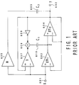
- Fig. 1 is a circuit diagram of a conventional filter circuit.
- the filter circuit is composed of two g m amplifiers 603 and 604 each for converting voltage to current, two variable gain amplifiers 605 and 607 each for changing gain, a NOT gate 608, an adder 609, and two capacitors 610 and 606.
- a non-inversion (+) input end of the g m amplifier (whose mutual conductance is g m1 ) 603 is connected to a signal input terminal 601, and an inversion (-) input end of the same g m amplifier 603 is connected to an output end of the g m amplifier (whose mutual conductance is g m2 ) 604 and a signal output terminal 602. Further, a non-inversion (+) input end of the g m amplifier 604 is connected to an output end of the g m amplifier 603, and an inversion (-) input end of the g m amplifier 604 is connected to the signal output terminal 602.
- variable gain amplifier 605 (whose gain is m) is connected to the signal input terminal 601, and an output end of the same variable gain amplifier 605 is connected to the signal output terminal 602 via a capacitor (whose capacitance is C 2 ) 606.
- a non-inversion (+) input end of the variable gain amplifier 607 (whose gain is n) 607 is connected to the output end of the g m amplifier 604, and an inversion (-) input end of the same variable gain amplifier 607 is connected to the signal input terminal 601.
- an input end of the NOT gate 608 is connected to the output end of the g m amplifier 604.
- variable gain amplifier 607 and the NOT gate 608 are both connected to two input ends of the adder 609, respectively.
- An output end of this adder 609 is connected to the non-inversion (+) input end of the g m amplifier 604 and the output end of the g m amplifier 603 via capacitor (whose capacitance is C 1 ) 610.
- the above formula (5) indicates that when the frequency is zero hertz, the group delay rate ⁇ is determined constant irrespective of the gains m and n of the two variable gain amplifiers 605 and 607. This implies that whenever the aperture control (APCONT) is adjusted for picture quality adjustment, the signal delay time hardly changes.
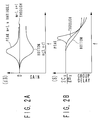
- Fig. 2A represents the gain characteristics obtained in accordance with the formula (3)
- Fig. 2B represents the group delay characteristics obtained in accordance with the formula (4), respectively.
- the group delay characteristics of the filter circuit are constant in a low frequency range.
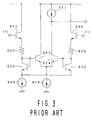
- Fig. 3 is a circuit diagram showing an example of the g m amplifier. As shown, a single g m amplifier consists of six bipolar transistors 801 to 806, two resistors elements 807 and 808, and three constant current circuits 809 to 811.
- the coefficients of the filter circuit can be decided on the basis of g m2 /C 2 and (g m1 .g m2 ) /(C 1 .C 2 ) in accordance with the transfer function as expressed by the formula (2). Accordingly, in order to reduce the capacitances of the two capacitors 606 and 610, it is necessary to also reduce the mutual conductances g m1 and g m2 . Therefore, the g m amplifier as shown in Fig.
- r e is an emitter resistance value of each of the bipolar transistors 801, 802, 805 and 806 and R is a resistance value of each of the resistors 807 and 808.
- capacitances of the capacitors 606 and 610 can be increased by r e /(R +2r e ) times, it is possible to reduce the area occupied by these capacitors 606 and 610 to that extent.
- the present invention provides a filter circuit having a signal input terminal and a signal output terminal, comprising: a first buffer having an input end connected to a first resistor and to a first capacitor; a second capacitor having one end connected to an output end of the first buffer; a second resistor having one end connected to the signal input terminal; a second buffer having an input end connected to the other end of the second resistor and to the other end of the second capacitor, and an output end connected to the signal output terminal; first signal supplying means for supplying a signal proportional to a difference between an output signal of the second buffer and a signal inputted from the signal input terminal, to the input end of the first buffer through the first resistor; and second signal supplying means for supplying a signal proportional to the signal inputted from the signal input terminal, to the input end of the first buffer through the first capacitor.
- the first signal supplying means may include an inverter for inverting the signal inputted from the signal input terminal to output an inverted signal; an adder for adding the inverted signal and the output signal of the second buffer to output an added signal; and an amplifier for amplifying the added signal by a predetermined times to output an amplified signal, the amplified signal being supplied to the input end of the first buffer through the first resistor.
- the first signal supplying means may include a differential amplifier having a non-inversion input end connected to the output end of the second buffer, and an inversion input end connected to the signal input terminal, an output signal of the differential amplifier being supplied to the input end of the first buffer through the first resistor.
- the first resistor may consist of a third resistor and a fourth resistor connected in parallel to each other; and the first signal supplying means may include first signal amplifying means for amplifying the signal inputted from the signal input terminal to output a first amplified signal, the first amplified signal being supplied to the input end of the first buffer through the third resistor; and second signal amplifying means for amplifying the output signal of the second buffer to output a second amplified signal, the second amplified signal being supplied to the input end of the first buffer through the fourth resistor.
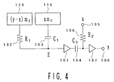
- Fig. 4 is a circuit diagram for assistance in explaining the concept of the filter circuit according to the present invention.
- an input end of a first buffer 101 is connected to one end of a first resistor (R 1 ) 102 and an end of a first capacitor (C 1 ) 103. Further, an output end of this buffer 101 is connected to an end of a second capacitor (C 2 ) 104. An end of a second resistor (R2) 106 is connected to a signal input terminal 105.
- An input end of a second buffer 107 is connected to the other end of the second capacitor (C 2 ) 104 and the other end of the second resistor (R 2 ) 106. Further, an output end of the second buffer 107 is connected to a signal output terminal 108.
- a first signal supplying section 109 amplifies a difference in voltage level between an input signal x of the signal input terminal 105 and an output signal y of the signal output terminal 108 (i.e., the output end of the second buffer 107) by m 1 times and supplies the amplified signal to the input end of the first buffer 101 via the first resistor (R 1 ) 102.
- a second signal supplying section 110 amplifies the input signal x of the signal input terminal 105 by m 2 times and supplies the amplified signal to the input end of the first buffer 101 via the first capacitor (C 1 ) 103.
- the above formula (10) indicates that when the frequency is zero hertz, the group delay rate ⁇ (0) is determined constant irrespective of the gains m 1 and m 2 of the first and second signal supplying sections 109 and 110.
- Fig. 5A represents the gain characteristics obtained in accordance with the formula (8)
- Fig. 5B represents the group delay characteristics obtained in accordance with the formula (9), respectively.
- the gain characteristics of the same filter circuit have a curve having a bottom value under the following conditions: m 2 ⁇ 1 k 1 k 2 ⁇ m 1 ⁇ 2 k 1 + k 2 2 k 2
- the peak value and the bottom value of the gain characteristics can be adjusted by changing the gain m 1
- the attenuation rate of the gain characteristics can be adjusted by changing the gain m 2 .
- both the gain and group delay characteristics shown in Figs. 2A and 2B, and 5A and 5B are quite similar with respect to each other.
- the filter circuit according to the present invention it is possible to obtain quite the same characteristics as those of the conventional filter circuit.
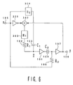
- the first signal supplying section 109 shown in Fig. 4 is constructed by a NOT gate (inverter) 301, an adder 302, and a variable gain amplifier 303.
- the NOT gate 301 inverts the signal x applied to its input end from the signal input terminal 105.
- the adder 302 adds the inverted output signal -x of the NOT gate 301 to an output signal y of the buffer 107, so that an addition signal (y-x) can be outputted by the adder 302.
- the variable gain amplifier 303 amplifies the output signal (y-x) of the adder 302 by m 1 times and supplies the amplified signal (y-x)m 1 to the buffer 101 via resistor (R 1 ) 102.
- the second signal supplying section 110 shown in Fig. 4 is constructed by a variable gain amplifier 304.
- the variable gain amplifier 304 amplifies the output signal x applied to its input end from the signal input terminal 105 by m 2 times and supplies the amplified signal xm 2 to the input end of the buffer 101 via capacitor (C 1 ) 103.
- the filter circuit according to the present invention since no g m amplifier is used, the number of elements which deteriorate S/N ratio can be reduced, as compared with the prior art filter circuit as shown in Fig. 1, with the result that it is possible to decrease the area occupied by the filter circuit.
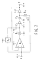
- the first signal supplying section 109 shown in Fig. 4 is constructed by a differential amplifier 401.
- the output signal y of the buffer 107 is inputted to a non-inversion (+) input end of the differential amplifier 401
- the signal x of the signal input terminal 105 is inputted to an inversion (-) input end of the differential amplifier 401. Therefore, the differential amplifier 401 amplifies a difference (y-x) between the output signal y of the buffer 107 and the input signal x of the signal input terminal 105 by m 1 times, and supplies the amplified signal (y-x)m 1 to the input end of the buffer 101 via resistor (R 1 ) 102.
- the second signal supplying section 110 shown in Fig. 4 is constructed by a variable gain amplifier 402.
- the variable gain amplifier 402 amplifies the output signal x applied from the signal input terminal 105 by m 2 times and supplies the amplified signal xm 2 to the input end of the buffer 101 via capacitor (C 1 ) 103.
- the first signal supplying section 109 shown in Fig. 4 is constructed by a variable gain amplifier 501 and another variable gain amplifier 503.
- the variable gain amplifier 501 amplifies the input signal x of the signal input terminal 105 by m 3 times, and supplies the amplified signal to the input end of the buffer 101 via resistor (R 3 ) 502.
- the second variable gain amplifier 503 amplifies the input signal x of the signal input terminal 105 by m 4 times, and supplies the amplified signal to the input end of the buffer 101 via resistor (R 4 ) 502.
- the second signal supplying section 110 shown in Fig. 4 is constructed by a variable gain amplifier 505.
- the variable gain amplifier 505 amplifies the input signal x of the signal input terminal 105 by m 2 times and supplies the amplified signal xm 2 to the input end of the buffer 101 via capacitor (C 1 ) 103.
- the filter circuit according to the present invention since no g m amplifier is used, the number of elements which deteriorate S/N ratio can be reduced, as compared with the conventional filter circuit as shown in Fig. 1, with the result that it is possible to decrease the occupied area of the filter circuit.
- the number of elements that consist of the conventional filter circuit shown in Fig. 1 is about 43 elements because two g m amplifiers (Fig. 3) are used.
- the number of elements that consist of the filter circuits shown in Figs. 6, 7, and 8 are about 25, 20, and 27 elements, respectively.
- the filter circuit according to the present invention it is possible to provide a filter circuit of a small circuit area and a high S/N ratio, without degrading the gain characteristics and the group delay characteristics of the filter circuit.
Landscapes
- Networks Using Active Elements (AREA)
Applications Claiming Priority (2)
| Application Number | Priority Date | Filing Date | Title |
|---|---|---|---|
| JP102752/95 | 1995-04-26 | ||
| JP10275295A JP3151376B2 (ja) | 1995-04-26 | 1995-04-26 | フィルタ回路 |
Publications (2)
| Publication Number | Publication Date |
|---|---|
| EP0740412A2 true EP0740412A2 (fr) | 1996-10-30 |
| EP0740412A3 EP0740412A3 (fr) | 1997-01-02 |
Family
ID=14335952
Family Applications (1)
| Application Number | Title | Priority Date | Filing Date |
|---|---|---|---|
| EP96106620A Withdrawn EP0740412A3 (fr) | 1995-04-26 | 1996-04-26 | Circuit de filtrage |
Country Status (5)
| Country | Link |
|---|---|
| US (1) | US5703523A (fr) |
| EP (1) | EP0740412A3 (fr) |
| JP (1) | JP3151376B2 (fr) |
| KR (1) | KR100186796B1 (fr) |
| TW (1) | TW299528B (fr) |
Families Citing this family (4)
| Publication number | Priority date | Publication date | Assignee | Title |
|---|---|---|---|---|
| JP4546627B2 (ja) * | 2000-08-29 | 2010-09-15 | 旭化成エレクトロニクス株式会社 | フィルタ中心周波数調整装置および方法 |
| DE10333108A1 (de) * | 2003-07-21 | 2005-03-03 | Schmidt, Peter | Anschlussvorrichtung für Computer-Peripheriegeräte |
| KR101324197B1 (ko) | 2007-09-17 | 2013-11-06 | 삼성전자주식회사 | 이퀄라이저 용 필터 |
| CN104485929A (zh) * | 2014-11-21 | 2015-04-01 | 成都嵌智捷科技有限公司 | 接收信号灵敏的驱动电路 |
Family Cites Families (10)
| Publication number | Priority date | Publication date | Assignee | Title |
|---|---|---|---|---|
| US3792367A (en) * | 1972-05-01 | 1974-02-12 | Bell Telephone Labor Inc | Active controllable filter circuit using variable transconductance amplifier |
| US4719512A (en) * | 1983-10-18 | 1988-01-12 | Kabushiki Kaisha Toshiba | Noise cancelling image sensor |
| JP2542634B2 (ja) * | 1987-09-08 | 1996-10-09 | 株式会社東芝 | アクティブフィルタ型信号調整回路 |
| JPH03172014A (ja) * | 1989-11-30 | 1991-07-25 | Toshiba Corp | アクティブ・フィルタ |
| JPH04180405A (ja) * | 1990-11-15 | 1992-06-26 | Toshiba Corp | フィルタ回路 |
| DE4038111A1 (de) * | 1990-11-29 | 1992-06-04 | Thomson Brandt Gmbh | Universalfilter |
| JPH04230110A (ja) * | 1990-12-27 | 1992-08-19 | Toshiba Corp | アクティブフィルタ回路 |
| JP3349550B2 (ja) * | 1993-05-31 | 2002-11-25 | トウシバビデオプロダクツ プライベート リミテッド | フィルタ回路 |
| JP3005413B2 (ja) * | 1994-01-26 | 2000-01-31 | 三洋電機株式会社 | フィルタ回路 |
| JPH07245546A (ja) * | 1994-03-03 | 1995-09-19 | Nippon Motorola Ltd | アクティブローパスフィルタ |
-
1995
- 1995-04-26 JP JP10275295A patent/JP3151376B2/ja not_active Expired - Fee Related
-
1996
- 1996-04-24 KR KR1019960012594A patent/KR100186796B1/ko not_active Expired - Fee Related
- 1996-04-26 US US08/641,076 patent/US5703523A/en not_active Expired - Fee Related
- 1996-04-26 EP EP96106620A patent/EP0740412A3/fr not_active Withdrawn
- 1996-05-31 TW TW085106522A patent/TW299528B/zh active
Also Published As
| Publication number | Publication date |
|---|---|
| TW299528B (fr) | 1997-03-01 |
| EP0740412A3 (fr) | 1997-01-02 |
| US5703523A (en) | 1997-12-30 |
| KR100186796B1 (ko) | 1999-04-15 |
| JPH08298436A (ja) | 1996-11-12 |
| JP3151376B2 (ja) | 2001-04-03 |
| KR960039609A (ko) | 1996-11-25 |
Similar Documents
| Publication | Publication Date | Title |
|---|---|---|
| EP0607702A2 (fr) | Un amplificateur d'égalisation variable | |
| JP2830087B2 (ja) | 周波数特性補正回路 | |
| JPH0474882B2 (fr) | ||
| US4521741A (en) | Impedance transformer circuit | |
| EP0740412A2 (fr) | Circuit de filtrage | |
| JP2542634B2 (ja) | アクティブフィルタ型信号調整回路 | |
| US4071782A (en) | Phaseless equalizer | |
| US4961057A (en) | Automatic gain control amplifier for compensating cable loss | |
| JPS5834046B2 (ja) | 橋絡t形可変等化器 | |
| US5113144A (en) | Feed-back type emphasis circuit | |
| US5805031A (en) | Transistor ratio controlled CMOS transmission line equalizer | |
| EP0696104B1 (fr) | Filtre passe-bande actif | |
| US4456885A (en) | Filter circuit suitable for being fabricated into integrated circuit | |
| US5394113A (en) | High impedance low-distortion linear amplifier | |
| JP3308352B2 (ja) | 可変遅延回路 | |
| JPS61170113A (ja) | 2次アクテイブ位相等価器 | |
| JP3349550B2 (ja) | フィルタ回路 | |
| JP3096131B2 (ja) | フィルタ回路 | |
| JP2658102B2 (ja) | 周波数特性調整回路 | |
| JP3109128B2 (ja) | シャープネス回路 | |
| US6816005B2 (en) | All pass filter | |
| JP3099679B2 (ja) | 低域ろ波回路 | |
| JP3111838B2 (ja) | 波形等化装置 | |
| JP3393240B2 (ja) | アクティブバンドパスフィルタ及びこれを用いた記録情報再生装置 | |
| JP2937653B2 (ja) | 周波数特性調整回路 |
Legal Events
| Date | Code | Title | Description |
|---|---|---|---|
| PUAI | Public reference made under article 153(3) epc to a published international application that has entered the european phase |
Free format text: ORIGINAL CODE: 0009012 |
|
| 17P | Request for examination filed |
Effective date: 19960426 |
|
| AK | Designated contracting states |
Kind code of ref document: A2 Designated state(s): DE FR GB |
|
| PUAL | Search report despatched |
Free format text: ORIGINAL CODE: 0009013 |
|
| AK | Designated contracting states |
Kind code of ref document: A3 Designated state(s): DE FR GB |
|
| 17Q | First examination report despatched |
Effective date: 19990723 |
|
| STAA | Information on the status of an ep patent application or granted ep patent |
Free format text: STATUS: THE APPLICATION IS DEEMED TO BE WITHDRAWN |
|
| 18D | Application deemed to be withdrawn |
Effective date: 19991204 |