EP0741353B1 - Système d'ordinateur avec entrée de données par crayon et effacement - Google Patents
Système d'ordinateur avec entrée de données par crayon et effacement Download PDFInfo
- Publication number
- EP0741353B1 EP0741353B1 EP96302193A EP96302193A EP0741353B1 EP 0741353 B1 EP0741353 B1 EP 0741353B1 EP 96302193 A EP96302193 A EP 96302193A EP 96302193 A EP96302193 A EP 96302193A EP 0741353 B1 EP0741353 B1 EP 0741353B1
- Authority
- EP
- European Patent Office
- Prior art keywords
- stylus
- digitizer
- writing
- display
- erasing
- Prior art date
- Legal status (The legal status is an assumption and is not a legal conclusion. Google has not performed a legal analysis and makes no representation as to the accuracy of the status listed.)
- Expired - Lifetime
Links
Images



Classifications
-
- G—PHYSICS
- G06—COMPUTING OR CALCULATING; COUNTING
- G06F—ELECTRIC DIGITAL DATA PROCESSING
- G06F3/00—Input arrangements for transferring data to be processed into a form capable of being handled by the computer; Output arrangements for transferring data from processing unit to output unit, e.g. interface arrangements
- G06F3/01—Input arrangements or combined input and output arrangements for interaction between user and computer
- G06F3/048—Interaction techniques based on graphical user interfaces [GUI]
- G06F3/0487—Interaction techniques based on graphical user interfaces [GUI] using specific features provided by the input device, e.g. functions controlled by the rotation of a mouse with dual sensing arrangements, or of the nature of the input device, e.g. tap gestures based on pressure sensed by a digitiser
- G06F3/0488—Interaction techniques based on graphical user interfaces [GUI] using specific features provided by the input device, e.g. functions controlled by the rotation of a mouse with dual sensing arrangements, or of the nature of the input device, e.g. tap gestures based on pressure sensed by a digitiser using a touch-screen or digitiser, e.g. input of commands through traced gestures
-
- G—PHYSICS
- G06—COMPUTING OR CALCULATING; COUNTING
- G06F—ELECTRIC DIGITAL DATA PROCESSING
- G06F3/00—Input arrangements for transferring data to be processed into a form capable of being handled by the computer; Output arrangements for transferring data from processing unit to output unit, e.g. interface arrangements
- G06F3/01—Input arrangements or combined input and output arrangements for interaction between user and computer
- G06F3/03—Arrangements for converting the position or the displacement of a member into a coded form
- G06F3/033—Pointing devices displaced or positioned by the user, e.g. mice, trackballs, pens or joysticks; Accessories therefor
- G06F3/0354—Pointing devices displaced or positioned by the user, e.g. mice, trackballs, pens or joysticks; Accessories therefor with detection of two-dimensional [2D] relative movements between the device, or an operating part thereof, and a plane or surface, e.g. 2D mice, trackballs, pens or pucks
- G06F3/03545—Pens or stylus
-
- G—PHYSICS
- G06—COMPUTING OR CALCULATING; COUNTING
- G06F—ELECTRIC DIGITAL DATA PROCESSING
- G06F3/00—Input arrangements for transferring data to be processed into a form capable of being handled by the computer; Output arrangements for transferring data from processing unit to output unit, e.g. interface arrangements
- G06F3/01—Input arrangements or combined input and output arrangements for interaction between user and computer
- G06F3/03—Arrangements for converting the position or the displacement of a member into a coded form
- G06F3/033—Pointing devices displaced or positioned by the user, e.g. mice, trackballs, pens or joysticks; Accessories therefor
- G06F3/038—Control and interface arrangements therefor, e.g. drivers or device-embedded control circuitry
- G06F3/0383—Signal control means within the pointing device
Definitions
- This invention relates to the interaction between computers and users and, more particularly, to intuitive graphical interfaces which allow the user to write and erase using a hand-held stylus on an electronic display.
- an erase function is needed to complement the write function.
- an eraser is conveniently located opposite the writing end of the pencil, and the user merely has to invert the pencil to use it. Such simplicity should also characterize the electronic equivalent.
- Farel et al discloses a self-contained stylus with physical writing and erasing ends. This is used in conjunction with an actual drawing board. However, an electronic grid under the board picks up signals from the stylus as it is writing (or erasing) and sends these to a computer for recording or other use.
- the stylus is an active device powered with an internal battery.
- EP-A-0 622 753 a stylus for writing and erasing is used in conjunction with an electrostatic tablet and an erase function is provided by electromagnetic coupling.
- EP-A-0 229 637 an erasing function is provided magnetically.
- a handheld computing device is provided with a planar electronic display, preferably a liquid-crystal screen. Directly above the screen is a transparent, planar digitizer which is stimulated by pressing on its surface. Both the display and the digitizer are part of a microprocessor-based system. The hardware and software of this system are arranged so that, in a common mode of operation, the display reproduces the path of a moving stylus pressing on the surface of the digitizer. This action simulates handwriting or drawing. Other modes of operation are also available, such as presenting the user with control "buttons" to press.
- an erase function is also provided.
- the stylus has both a writing end and an erasing end, similiar to a pencil.
- the system removes any graphical traces under the stylus in a manner closely resembling rubber erasure of pencil traces on paper, except that multiple passes are not needed for complete removal of the traces.
- an inductive winding preferably in the form of a planar spiral.
- the erasing end of the stylus contains a permanent magnet with a localized field.
- an AC voltage is induced in the winding.
- This AC signal is conditioned to provide an ERASE ENABLE signal to the microprocessor.
- ERASE ENABLE is present AND there is a digitizer signal, the system erases any graphical trace in the neighborhood indicated by the digitizer. Thus a trace may be removed by moving the stylus across the digitizer surface above the trace. Likewise a single point may be erased by moving the stylus toward, and then contacting, the digitizer.
- Fig. 1 is a layout diagram of the graphics elements of the system, together with the sensing inductive winding.
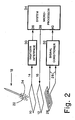
- Fig. 2 is a block diagram of the preferred embodiment of the invention.
- Fig. 3 is a diagram showing a preferred topology of the inductive winding plus circuit elements of a signal conditioner.
- Fig. 4 is a diagram of a digitizer interface circuit.
- a planar graphical display 12 is overlaid with a transparent planar digitizer 10.
- display 12 is a liquid crystal type, although other varieties, such as electroluminescent, could be used if higher power consumption is tolerable.
- Digitizer 10 is composed of layers of both electrically conductive and insulating material. These are arranged so that, when the digitizer surface is pressed, resistances measurable on cable 14 can be interpreted to determine the surface position where the pressure was applied. Both digitizer 10 and display 12 have active areas nominally the same size, and these active areas are superimposed in the assembled computer.
- Cable 16 supplies drive signals to display 12, enabling the generation or removal of image elements ("pixels") anywhere on the active area of the display. Cable 16 connects to the system microprocessor, not shown in this figure, while cable 14 connects to a digitizer interface circuit, also not shown. Further details and illustrations of these devices will be set forth below.
- the computer has a user-input device, stylus 18, for signalling the system via digitizer 10.
- This simple, passive device has a pointed writing end 20 and an erasing end 22. Secured to the erasing end is a permanent magnet, whose (invisible) magnetic field is symbolically represented by the dotted lines 24.
- winding 26 Directly under display 12 is an inductive winding 26.
- the size and location of this winding makes it responsive to a magnetic field applied anywhere in the active areas of digitizer 10 and display 12.
- winding 26 is illustrated by the well-recognized circular solenoid symbol. In practice, it is likely to be a planar winding, as illustrated in other figures in the disclosure. Connections 28 from winding 26 are coupled to a signal conditioner later explained and illustrated.
- Fig. 2 shows additional elements of the handheld computer.
- a digitizer interface circuit 30 is needed to convert the variable resistance values from the digitizer into data words readable by the system microprocessor 34. Interface 30 sends these words to the processor port 36.
- Fig. 4 shows circuitry for implementing interface 30, and its operation is explained below.
- Processor 34 drives display 12 via port 38 and cable 16. Sometimes scanning circuits, external to the processor, are used to drive displays. However, for a handheld device, the display driving task can usually be done entirely by the processor, as is indicated here.
- erasing is defined by combination 5. That is, the processor should be programmed to remove graphical traces in the vicinity indicated by the digitizer during combination 5.
- the radius of erasure can, conveniently, be set by the user according to the complexity and fine structure of the graphic material.
- an additional event may also invoke erasure: if combination 2 transitions to combination 4, this can indicate the user's desire to erase a single point or a chosen, circular area around such a point.
- signal conditioner 32 The operation of signal conditioner 32 may be appreciated by reference to Fig. 3 and the following comments.
- the function of signal conditioner 32 is to convert the small, magnetically induced signal in winding 26 into a (typically) TTL logic signal ERASE ENABLE to be supplied to processor port 40.
- winding 26 is shown as a planar, rectangular, spiral inductance. Preferably, this inductance is created by etching its pattern on a printed circuit board. Its sensitivity to a small, varying magnetic field is nominally constant over its area, with local maxima in the neighborhood of each conductor.
- the signal in winding 26 is supplied to a DC-coupled amplifier 40, which amplifies it to an average level of about 3 volts RMS. (For use inside buildings, amplifier 40 should have negligible response to powerline frequencies.)
- This rectified signal then passes through lowpass filter 42, whose cutoff frequency is about 10 Hz.
- the optimum frequency should be determined experimentally, as it depends on the size and pitch of winding 26, the strength of stylus magnetic field 24, and other factors difficult to quantify.
- Output from lowpass 42 is then supplied to a comparator 42, where it is compared against a reference threshold voltage Vth and translated to TTL logic levels. The optimum value of Vth should be determined experimentally.
- the output from comparator 42 is the ERASE ENABLE logic signal used to distinguish states 1, 3, and 4 from states 2 and 5 in the above table.
- Digitizer 10 is represented electrically as two variable resistors Rx and Ry.
- the values of these resistors represent the X and Y coordinates, respectively, of the stylus position.
- These resistance values are converted into voltages by current sources Ix (52) and Iy (50). Multiplexing is used to conserve circuitry: these voltages are converted, in repetitive sequence, to digital words by A/D converter 56.
- the sequencing is handled by a control signal from processor 34, which arrives from port 36 on line 58.
- the control signal operates multiplexer 54 and enables conversion in A/D 56.
- a sequencing rate of at least 100 Hz is usually adequate to generate X and Y sample value trains characterizing the successive positions of stylus 18.
- A/D 56 supplies 8- or 10-bit words to processor 34 via line 60 and port 36.
Landscapes
- Engineering & Computer Science (AREA)
- General Engineering & Computer Science (AREA)
- Theoretical Computer Science (AREA)
- Human Computer Interaction (AREA)
- Physics & Mathematics (AREA)
- General Physics & Mathematics (AREA)
- Position Input By Displaying (AREA)
- Character Discrimination (AREA)
Claims (10)
- Procédé d'effacement d'une partie d'un système d'écriture électronique à base de stylet, système comprenant un numériseur (10) traversé par un stylet d'écriture (18) et un affichage électronique (12) fournissant une image du trajet du stylet en travers du numériseur, un aimant permanent étant fixé à une extrémité d'effacement (22) du stylet à l'opposé d'une extrémité d'écriture (20), et un bobinage inductif (26) étant positionné conjointement au numériseur, procédé comprenant :a) la mise en contact du numériseur avec l'extrémité d'effacement du stylet ;b) le contrôle du bobinage inductif afin de constater la présence d'un signal induit à l'intérieur par déplacement de l'aimant permanent ; etc) l'effacement d'une partie de l'image indiqué par le trajet de l'extrémité d'effacement en travers du numériseur lorsqu'il existe un signal présent, de façon simultanée, dans le bobinage inductif.
- Procédé d'effacement selon la revendication 1, selon lequel, dans le système, l'affichage (12) est positionné, de même, de façon conjointe au bobinage inductif (26) et au numériseur (10).
- Système d'écriture électronique à base de stylet possédant, à la fois, des fonctions d'écriture et d'effacement, comprenant :a) un stylet d'écriture (18) possédant une extrémité d'écriture (20) et une extrémité d'effacement (22) et un aimant permanent fixé sur l'extrémité d'effacement ;b) un numériseur (10) possédant une surface d'écriture et une sortie (14) pour des signaux indiquant une position sur la surface d'écriture touchée par le stylet ;c) un affichage électronique (12) possédant une entrée d'attaque (16) ;d) un circuit d'attaque d'affichage (34) possédant une entrée (36) couplée à la sortie du numériseur, une entrée de VALIDATION d'EFFACEMENT (40) et une sortie d'attaque (38) couplée à l'entrée d'attaque d'affichage ;e) un bobinage inductif (26) similaire en dimension au numériseur et proche du numériseur ; etf) un circuit de conditionnement (32) possédant une entrée couplée au bobinage inductif et une sortie couplée à l'entrée de VALIDATION d'EFFACEMENT.
- Système d'écriture électronique à base de stylet selon la revendication 3, dans lequel le stylet d'écriture (18) est un dispositif passif.
- Système d'écriture électronique à base de stylet selon la revendication 3, dans lequel le circuit d'attaque d'affichage (34) est incorporé dans un microprocesseur commandant le système d'écriture.
- Système d'écriture électronique à base de stylet selon la revendication 3, dans lequel le numériseur (14) comprend des feuilles conductrices sensibles à la pression possédant des signaux de sortie X et Y.
- Système d'écriture électronique à base de stylet selon la revendication 3, dans lequel le bobinage inductif (26) est une spirale plane.
- Système d'écriture électronique à base de stylet selon la revendication 3, dans lequel l'affichage électronique (12) est similaire en dimension au numériseur (10) et est positionné conjointement à ce dernier.
- Système d'écriture électronique à base de stylet selon la revendication 3, dans lequel le numériseur (10) est transparent, l'affichage électronique (12) est proche d'une surface du numériseur opposée à la surface d'écriture, et le bobinage inductif (26) est similaire en dimension à l'affichage et est positionné conjointement à ce dernier.
- Système d'écriture électronique à base de stylet selon la revendication 9, dans lequel le numériseur (10), l'affichage (12) et le bobinage inductif (26) sont des dispositifs plans.
Applications Claiming Priority (2)
| Application Number | Priority Date | Filing Date | Title |
|---|---|---|---|
| US433771 | 1995-05-03 | ||
| US08/433,771 US5654529A (en) | 1995-05-03 | 1995-05-03 | Stylus-input computing system with erasure |
Publications (2)
| Publication Number | Publication Date |
|---|---|
| EP0741353A1 EP0741353A1 (fr) | 1996-11-06 |
| EP0741353B1 true EP0741353B1 (fr) | 2001-06-20 |
Family
ID=23721474
Family Applications (1)
| Application Number | Title | Priority Date | Filing Date |
|---|---|---|---|
| EP96302193A Expired - Lifetime EP0741353B1 (fr) | 1995-05-03 | 1996-03-28 | Système d'ordinateur avec entrée de données par crayon et effacement |
Country Status (4)
| Country | Link |
|---|---|
| US (1) | US5654529A (fr) |
| EP (1) | EP0741353B1 (fr) |
| JP (1) | JP3786464B2 (fr) |
| DE (1) | DE69613429T2 (fr) |
Families Citing this family (35)
| Publication number | Priority date | Publication date | Assignee | Title |
|---|---|---|---|---|
| US6512513B2 (en) * | 1919-04-01 | 2003-01-28 | Wacom Co., Ltd. | Pointer for use in digitizer systems |
| US5793360A (en) * | 1995-05-05 | 1998-08-11 | Wacom Co., Ltd. | Digitizer eraser system and method |
| US6259043B1 (en) | 1996-01-23 | 2001-07-10 | International Business Machines Corporation | Methods, systems and products pertaining to a digitizer for use in paper based record systems |
| US6707451B1 (en) * | 1996-09-11 | 2004-03-16 | Pilot Precision Kabushiki Kaisha | Input pen |
| KR100209603B1 (ko) * | 1996-12-23 | 1999-07-15 | 구자홍 | 위치검출 액정 디스플레이장치 |
| US7616198B2 (en) * | 1998-02-20 | 2009-11-10 | Mental Images Gmbh | System and computer-implemented method for modeling the three-dimensional shape of an object by shading of a two-dimensional image of the object |
| EP0980038A3 (fr) | 1998-08-13 | 2002-11-20 | Motorola, Inc. | Appareil et procédé pour présenter simultanément dans la même région d'une interface utilisateur des caractères de texte et des caractères manuscrits |
| US6326945B1 (en) | 1999-12-13 | 2001-12-04 | Williams, Iii Carl K. | Magnetic writing board |
| US6473552B1 (en) * | 2000-05-01 | 2002-10-29 | 3Com Corporation | Apparatus and method for signaling using a light pipe stylus |
| WO2002043045A1 (fr) * | 2000-11-22 | 2002-05-30 | Cirque Corporation | Dispositif d'entree de stylet a aimant permanent |
| US20030095115A1 (en) * | 2001-11-22 | 2003-05-22 | Taylor Brian | Stylus input device utilizing a permanent magnet |
| US20030117378A1 (en) | 2001-12-21 | 2003-06-26 | International Business Machines Corporation | Device and system for retrieving and displaying handwritten annotations |
| US6980202B2 (en) * | 2001-12-21 | 2005-12-27 | International Business Machines Corporation | Method and system for creating and accessing hyperlinks from annotations relating to a physical document |
| EP1413976A1 (fr) * | 2002-10-22 | 2004-04-28 | Nokia Corporation | Procédé et dispositif pour la sélection du mode d'entrée |
| US7310779B2 (en) * | 2003-06-26 | 2007-12-18 | International Business Machines Corporation | Method for creating and selecting active regions on physical documents |
| US7385594B2 (en) * | 2004-02-19 | 2008-06-10 | Au Optronics Corporation | Position encoded sensing device and a method thereof |
| US7426643B2 (en) * | 2004-06-22 | 2008-09-16 | Hewlett-Packard Development Company, L.P. | Input device feature |
| US20080030486A1 (en) * | 2006-08-04 | 2008-02-07 | Quiteso Technologies, Llc | Multi-functional pen input device |
| KR101135898B1 (ko) * | 2007-12-05 | 2012-04-13 | 삼성전자주식회사 | 리모트 컨트롤러 및 그 제어방법과 이를 가지는영상처리장치 |
| KR20090058721A (ko) | 2007-12-05 | 2009-06-10 | 헬스 앤드 라이프 컴퍼니 리미티드 | 에어로졸 발생장치 |
| TW200928887A (en) | 2007-12-28 | 2009-07-01 | Htc Corp | Stylus and electronic device |
| US20090267891A1 (en) * | 2008-04-25 | 2009-10-29 | Bamidele Ali | Virtual paper |
| US8243028B2 (en) * | 2008-06-13 | 2012-08-14 | Polyvision Corporation | Eraser assemblies and methods of manufacturing same |
| KR101443341B1 (ko) * | 2008-06-30 | 2014-11-03 | 엘지전자 주식회사 | 휴대 단말기 및 그 동작제어 방법 |
| JP5430339B2 (ja) | 2009-10-19 | 2014-02-26 | 株式会社ワコム | 位置検出装置及び位置指示器 |
| CN102156560A (zh) * | 2011-04-28 | 2011-08-17 | 中兴通讯股份有限公司 | 终端及利用手写笔正反两端在终端上输入不同操作的方法 |
| US9268416B2 (en) | 2011-08-05 | 2016-02-23 | Htc Corporation | Touch control pen, touching control apparatus and touching detection method with image delete function thereof |
| US9195351B1 (en) * | 2011-09-28 | 2015-11-24 | Amazon Technologies, Inc. | Capacitive stylus |
| TWI471764B (zh) * | 2012-02-20 | 2015-02-01 | Qisda Corp | 座標感測系統、座標感測方法及顯示系統 |
| EP3168717A4 (fr) * | 2014-07-11 | 2018-03-14 | Wacom Co., Ltd. | Indicateur de position, dispositif de détection de position et procédé de commande d'entrée pour dispositif de détection de position |
| EP3299936B1 (fr) | 2015-05-21 | 2020-01-01 | Wacom Co., Ltd. | Stylet actif |
| US9836136B2 (en) | 2015-09-18 | 2017-12-05 | Microsoft Technology Licensing, Llc | Voltage boost circuit for a stylus pen |
| TWM517860U (zh) * | 2015-10-16 | 2016-02-21 | 翰碩電子股份有限公司 | 具抹除器的電容筆 |
| CN108749407B (zh) * | 2018-04-26 | 2020-06-19 | 永康市智伴信息科技有限公司 | 一种书写机构及黑板 |
| CN109683372A (zh) * | 2019-01-30 | 2019-04-26 | 深圳市恒开源电子有限公司 | 一种具有局部擦除功能的液晶膜片及液晶书写装置 |
Family Cites Families (9)
| Publication number | Priority date | Publication date | Assignee | Title |
|---|---|---|---|---|
| JPS59107297U (ja) * | 1983-01-08 | 1984-07-19 | 富士通株式会社 | 電子黒板用消去器 |
| JPS59214700A (ja) * | 1983-05-21 | 1984-12-04 | 株式会社パイロット | Xyプロツタ装置 |
| FR2584836B1 (fr) * | 1985-07-09 | 1992-06-19 | Farel Alain | Procede de saisie informatique de donnees graphiques concomitante a leur creation |
| EP0229637A3 (fr) * | 1986-01-09 | 1988-10-05 | Wacom Co., Ltd. | Appareil de tableau électronique |
| EP0307893B1 (fr) * | 1987-09-14 | 1995-03-08 | Wacom Co., Ltd. | Système de tableau électronique avec un marqueur et un effaceur associés à ce tableau |
| US5231578A (en) * | 1988-11-01 | 1993-07-27 | Wang Laboratories, Inc. | Apparatus for document annotation and manipulation using images from a window source |
| EP0618715A4 (fr) * | 1991-12-13 | 1996-12-18 | Ace Denken Kk | Bloc-notes electronique. |
| US5401916A (en) * | 1992-09-29 | 1995-03-28 | Ncr Corporation | Method and apparatus for capturing handwritten information and providing visual feedback |
| US5475401A (en) * | 1993-04-29 | 1995-12-12 | International Business Machines, Inc. | Architecture and method for communication of writing and erasing signals from a remote stylus to a digitizing display |
-
1995
- 1995-05-03 US US08/433,771 patent/US5654529A/en not_active Expired - Lifetime
-
1996
- 1996-03-28 EP EP96302193A patent/EP0741353B1/fr not_active Expired - Lifetime
- 1996-03-28 DE DE69613429T patent/DE69613429T2/de not_active Expired - Lifetime
- 1996-04-04 JP JP8236596A patent/JP3786464B2/ja not_active Expired - Lifetime
Also Published As
| Publication number | Publication date |
|---|---|
| JP3786464B2 (ja) | 2006-06-14 |
| JPH08314636A (ja) | 1996-11-29 |
| US5654529A (en) | 1997-08-05 |
| DE69613429T2 (de) | 2001-10-25 |
| EP0741353A1 (fr) | 1996-11-06 |
| DE69613429D1 (de) | 2001-07-26 |
Similar Documents
| Publication | Publication Date | Title |
|---|---|---|
| EP0741353B1 (fr) | Système d'ordinateur avec entrée de données par crayon et effacement | |
| KR101113530B1 (ko) | 진동 감지 터치 입력 디바이스용 웨이크-온-터치 | |
| TW556108B (en) | Coordinate input device detecting touch on board associated with liquid crystal display, and electronic device therefor | |
| KR20020087993A (ko) | 정보 입력 장치 | |
| WO1997044901A1 (fr) | Unite peripherique d'entree pour ordinateur utilisable conjointement avec une unite d'entree pour souris | |
| CN107145248A (zh) | 一种触摸笔、触摸控制方法及触摸系统 | |
| US12613629B2 (en) | Handwriting input device | |
| US20200012359A1 (en) | Stylus button control | |
| JP2766101B2 (ja) | 表示付タブレット装置 | |
| KR101295356B1 (ko) | 필기감 제공 기능을 갖는 디지타이저 펜 및 구동 시스템 | |
| JPH07261906A (ja) | ペン入力方式データ処理装置 | |
| JPH08286830A (ja) | 手書き入力装置 | |
| CN114296572B (zh) | 触控式电子设备 | |
| JP2000132318A (ja) | 多機能ペン | |
| TWI300190B (fr) | ||
| CN114397970A (zh) | 一种触控笔、触控显示设备及其通信方法 | |
| JPH0350621A (ja) | 対話型の電子的書き込み/表示装置 | |
| CN117275320B (zh) | 一种大面幅便携盲文阅读器 | |
| JPH0232471Y2 (fr) | ||
| JPS6168626A (ja) | 画像入出力装置 | |
| CN112689814A (zh) | 笔迹清除工具、书写设备和书写系统 | |
| JPH0944304A (ja) | タッチパネル入力表示装置 | |
| JP2025167183A (ja) | パッド付属物、仮想入力デバイス、及び入力システム | |
| JP2001084087A (ja) | 手書入力装置 | |
| JPS61120229A (ja) | 描画モ−ド識別方式 |
Legal Events
| Date | Code | Title | Description |
|---|---|---|---|
| PUAI | Public reference made under article 153(3) epc to a published international application that has entered the european phase |
Free format text: ORIGINAL CODE: 0009012 |
|
| AK | Designated contracting states |
Kind code of ref document: A1 Designated state(s): DE FR GB IT |
|
| 17P | Request for examination filed |
Effective date: 19970411 |
|
| 17Q | First examination report despatched |
Effective date: 19990924 |
|
| GRAG | Despatch of communication of intention to grant |
Free format text: ORIGINAL CODE: EPIDOS AGRA |
|
| GRAG | Despatch of communication of intention to grant |
Free format text: ORIGINAL CODE: EPIDOS AGRA |
|
| GRAH | Despatch of communication of intention to grant a patent |
Free format text: ORIGINAL CODE: EPIDOS IGRA |
|
| GRAH | Despatch of communication of intention to grant a patent |
Free format text: ORIGINAL CODE: EPIDOS IGRA |
|
| RAP1 | Party data changed (applicant data changed or rights of an application transferred) |
Owner name: HEWLETT-PACKARD COMPANY, A DELAWARE CORPORATION |
|
| GRAA | (expected) grant |
Free format text: ORIGINAL CODE: 0009210 |
|
| ITF | It: translation for a ep patent filed | ||
| AK | Designated contracting states |
Kind code of ref document: B1 Designated state(s): DE FR GB IT |
|
| REF | Corresponds to: |
Ref document number: 69613429 Country of ref document: DE Date of ref document: 20010726 |
|
| ET | Fr: translation filed | ||
| REG | Reference to a national code |
Ref country code: GB Ref legal event code: IF02 |
|
| PLBE | No opposition filed within time limit |
Free format text: ORIGINAL CODE: 0009261 |
|
| STAA | Information on the status of an ep patent application or granted ep patent |
Free format text: STATUS: NO OPPOSITION FILED WITHIN TIME LIMIT |
|
| 26N | No opposition filed | ||
| REG | Reference to a national code |
Ref country code: GB Ref legal event code: 732E Free format text: REGISTERED BETWEEN 20110113 AND 20110119 |
|
| REG | Reference to a national code |
Ref country code: FR Ref legal event code: TP |
|
| REG | Reference to a national code |
Ref country code: DE Ref legal event code: R081 Ref document number: 69613429 Country of ref document: DE Owner name: SAMSUNG ELECTRONICS CO., LTD., SUWON-SI, KR Free format text: FORMER OWNER: HEWLETT-PACKARD DEVELOPMENT COMPANY, L.P., HOUSTON, TEX., US Effective date: 20110222 Ref country code: DE Ref legal event code: R081 Ref document number: 69613429 Country of ref document: DE Owner name: SAMSUNG ELECTRONICS CO., LTD., KR Free format text: FORMER OWNER: HEWLETT-PACKARD DEVELOPMENT CO., L.P., HOUSTON, US Effective date: 20110222 |
|
| REG | Reference to a national code |
Ref country code: FR Ref legal event code: PLFP Year of fee payment: 20 |
|
| PGFP | Annual fee paid to national office [announced via postgrant information from national office to epo] |
Ref country code: DE Payment date: 20150318 Year of fee payment: 20 Ref country code: IT Payment date: 20150225 Year of fee payment: 20 |
|
| PGFP | Annual fee paid to national office [announced via postgrant information from national office to epo] |
Ref country code: GB Payment date: 20150225 Year of fee payment: 20 Ref country code: FR Payment date: 20150320 Year of fee payment: 20 |
|
| REG | Reference to a national code |
Ref country code: DE Ref legal event code: R071 Ref document number: 69613429 Country of ref document: DE |
|
| REG | Reference to a national code |
Ref country code: GB Ref legal event code: PE20 Expiry date: 20160327 |
|
| PG25 | Lapsed in a contracting state [announced via postgrant information from national office to epo] |
Ref country code: GB Free format text: LAPSE BECAUSE OF EXPIRATION OF PROTECTION Effective date: 20160327 |