EP0741366B1 - Circuit de multiplication - Google Patents
Circuit de multiplication Download PDFInfo
- Publication number
- EP0741366B1 EP0741366B1 EP96106574A EP96106574A EP0741366B1 EP 0741366 B1 EP0741366 B1 EP 0741366B1 EP 96106574 A EP96106574 A EP 96106574A EP 96106574 A EP96106574 A EP 96106574A EP 0741366 B1 EP0741366 B1 EP 0741366B1
- Authority
- EP
- European Patent Office
- Prior art keywords
- output
- circuit
- input
- mos inverters
- inverting amplifier
- Prior art date
- Legal status (The legal status is an assumption and is not a legal conclusion. Google has not performed a legal analysis and makes no representation as to the accuracy of the status listed.)
- Expired - Lifetime
Links
Images




Classifications
-
- G—PHYSICS
- G06—COMPUTING OR CALCULATING; COUNTING
- G06F—ELECTRIC DIGITAL DATA PROCESSING
- G06F7/00—Methods or arrangements for processing data by operating upon the order or content of the data handled
- G06F7/38—Methods or arrangements for performing computations using exclusively denominational number representation, e.g. using binary, ternary, decimal representation
- G06F7/48—Methods or arrangements for performing computations using exclusively denominational number representation, e.g. using binary, ternary, decimal representation using non-contact-making devices, e.g. tube, solid state device; using unspecified devices
- G06F7/52—Multiplying; Dividing
-
- G—PHYSICS
- G06—COMPUTING OR CALCULATING; COUNTING
- G06J—HYBRID COMPUTING ARRANGEMENTS
- G06J1/00—Hybrid computing arrangements
Definitions
- the invention relates to a multiplication circuit according to the preamble part of claim 1.
- Such a multiplication circuit is described in EP 707 274 A1 and comprises a plurality of weighting circuits.
- Each weighting circuit comprises a plurality of switching means, a group of capacitors, an inverting amplifier and a feedback capacitor.
- Each switching means connects a capacitor of the capacitor group either to an input voltage or to ground voltage.
- the assignee of this invention proposes a multiplication circuit to multiply analog input voltage by digital multiplier in Japanese patent publication numbered 06-195483.
- the input voltage is connected to a capacitive coupling consisting of a plurality of parallel capacitances which are selectively connected to the input voltage by switches for weighting of the input voltage.
- a capacitive coupling consisting of a plurality of parallel capacitances which are selectively connected to the input voltage by switches for weighting of the input voltage.
- two stages of inverting amplifying portions in which feedback capacitances are connected to serial MOS inverters are connected and the linear characteristics of the output is guaranteed.
- this multiplication circuit has a problem that a large capacity of capacitance is necessary when a large multiplier is set and the area of the circuit becomes large because the weighting is performed only by the capacitances of capacitive coupling.
- input voltage Vin is connected through switch circuit SWC1 to a capacitive coupling CP1, whose output is input to an inverting amplifying portion INV1 as shown in Figure 6.
- the output of INV1 is input to a group CF1 of parallel feedback capacitances, whose output is connected to the input side of INV1 by switch circuit SWC2.
- Switch circuit SWC1 connects C11 to C14 of the capacitances of CP1 to Vin or a reference voltage
- switch circuit SWC2 connects the capacitors C21 to C24 of CF1 to the input of INV1 or the reference voltage.
- INV1 The output of INV1 is connected to a similar inverting amplifying portion INV2, through switch circuit SWC3 and capacitive coupling CP2 (consisting of C31, C32, C33 and C34).
- the input of INV2 is connected to its output through feedback capacitance group CF2 and switch circuit SWC4. Representing an output of INV1 by V', Vout of the output of INV2 can be expressed as in formula (2) in the same way above.
- Vout -V'• ⁇ C 3 i ⁇ C 4 i
- the output level is controlled by these weighting of formulas (1) and (2).
- the offset voltage is set off by setting SWC2 to SWC4 so that the effective composit capacities of CF1, CP2 and CF2 are the same, and by setting that (C11+C12+C13+C14) is equal to (C31+C32+C33+C34).
- the multiplier of the scaler circuit is defined according to the capacity of the capacitance.
- Preferred embodiments of the invention are the subject-matter of the dependent claims.
- One advantage of the present invention is that the product of multipliers of the successive multiplication circuits can be regarded as one multiplier thereby reducing the number of unit capacitances as well as circuit area.
- Another advantage of the present invention is that a first inverting amplifier and a second inverting amplifier cancel out each other's offset voltage.
- a further advantage of the present invention is an increased design flexibility.
- Figure 1 shows a circuit of the first embodiment of the multiplication circuit of the present invention.
- Figure 2 shows a circuit of the second embodiment as the scaler circuit.
- Figure 3 shows a circuit of the inverting amplifying portion in the second embodiment.
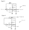
- Figure 4 shows a diagram of the reference voltage generating circuit in the second embodiment.
- Figure 5 shows a variation of the second embodiment.
- Figure 6 shows a conventional scaler circuit.
- the circuit includes a switch circuit having a plurality of switches of SW1, SW2, SW3 and SW4 parallelly connected to an input voltage.
- An output of the switch circuit is input to a capacitive coupling CP1 including a plurality of capacitances C1, C2, C3 and C4. That is, the outputs of each switch SW1, SW2, SW3 and SW4 is connected to capacitances C1, C2, C3 and C4, respectively.
- the capacitances are selectively connected by the switches to the input voltage.
- the inputs of switches SW1 to SW4 are alternatively connected to the input voltage or the ground, so Vin or 0V is impressed on the capacitances.
- An output of the capacitive coupling CP1 is input to an inverting amplifying portion I1.
- the voltage output of a capacitive coupling is transmitted to the next stage with good linearity and driving ability.
- Inverting amplifying portion I1 consists of three stages of MOS inverters I11, I12 and I13, serially connected. An output of MOS inverter I13 on the last stage is fed back to an input of I1 by a feedback capacitance CF1.
- the serial circuit of MOS inverters has a gain large enough. The input and output becomes coincident by feeding back the output to the input, consequently, it is possible to stably provide the inverted output of an input independently from the load of circuits on the next stage.
- MOS inverter I13 The output of MOS inverter I13 is connected to a grounded capacitance CG11, through which it is grounded.
- the output of MOS inverter I12 is connected to resistances RE11 and RE12.
- RE11 connects a supply voltage Vdd to the output of I12 and RE12 connects the output of I12to the ground.
- These resistances RE11 and RE12 forms balancing resistance in pairs and contribute to prevent unstable oscillation.
- the output of inverting amplifying portion 11 is input to the switch circuit consisting of a plurality of switches SW5, SW6, SW7 and SW8.
- the output of the inverting amplifying portion is connected to each switch in the switch circuit.
- An output of the switch circuit is input to a capacitive coupling CP2 consisting of a plurality of capacitances C5, C6, C7 and C8. That is, the outputs of switches SW5, SW6, SW7 and SW8 are connected to capacitances C5, C6, C7 and C8, respectively.
- the capacitances are selectively connected by switches to the output of the inverting amplifying portion I1.
- the output of capacitive coupling CP2 is input to an inverting amplifying portion I2.
- the voltage output of the capacitive coupling is transmitted to the next stage with good linearity and driving ability.
- inverting amplifying portion I2 three stages of MOS inverters I21, I22 and I23 are connected in serial. An output of the last stage of MOS inverter I23 is fed back to an input of I2 by a feedback capacitance CF2. Accordingly, the input of CP2 can be inverted and output with good linearity and driving ability similarly to I1.
- inverting amplifying portion I2 grounded capacitance CG21, balancing resistance RE21 and RE22 are connected as in I1, which prevent unstable oscillation.
- a grounded capacitance CG12 is connected parallelly with C1 to C4, an input of which is connected to the ground instead of Vin.
- a grounded capacitance CG22 is connected parallelly with C5 to C8, an input of which is connected to the ground instead of the output of I1.
- V1 of I1 is expressed in the formula (3).
- VI 1 + Vb - Vin ( C 1 + C 2 + C 3 + C 4) CF 1
- Vout of the output of I2 is as in the formula (4).
- Vout + Vb - VI 1( C 5 + C 6 + C 7 + C 8) CF 2
- the multiplication can be expressed by formula (8).
- Vout Vin ( ⁇ C 1 i • ⁇ C 2 i ) CF 1• CF 2
- the capacity of the capacitances can be prevented from being large and multiplication of large multipliers can be performed.
- the multiplication with a binary multiplier can be performed by setting the effective composite capacity.
- the capacitance C5 to C8 are similarly set.
- Grounded capacitances CG12 and CG22 are effective to control the maximum value of the multiplier and the linearity of the outputs can be improved.
- designing of the multiplier becomes easier when such grounded capacitances are omitted, there is a case to omit them in the actual circuit.
- the scaler circuit consists of a switch circuit SWC1, capacitive coupling CP1, inverting amplifying portion INV1, switch circuit SWC3, capacitive coupling CP2 and inverting amplifying portion INV2, connected in series.
- An input voltage Vin is connected to the switch circuit SWC1.
- Switch circuit SWC1 includes a plurality of switches SW1, SW2, SW3 and SW4 for alternatively connecting Vin or a reference voltage to its output.
- the reference voltage is generated by a reference voltage generating circuit Vref, and the half voltage of the common supply voltage Vdd, that is Vdd / 2 is generated in the whole circuit.
- Capacitive coupling CP1 is structured by integrating the outputs of capacitances C1, C2, C3 and C4 which are connected to switches SW1 to SW4, respectively.
- the output of CP1 is input to INV1.
- Switch circuit SWC1 alternatively impresses Vin or the reference voltage to each capacitance of capacitive coupling CP1, and the integrated outputs are input to INV1.
- a switch circuit SWC2 is connected, which consists of a plurality of switches SW5, SW6, SW7 and SW8 connected to INV1 in parallel.
- a group CF1 of feedback capacitances is connected, which consists of a plurality of capacitances C5, C6, C7 and C8 connected to SWC2 in parallel.
- the outputs of C5 to C8 are integrated and connected to the input of lNV1, and each switches from SW5 to SW8 alternatively connects the output of INV1 or the reference voltage to the corresponding capacitances among C5 to C8, respectively.
- reference voltage capacitance Cr1 is connected parallelly to capacitances from C1 to C4.
- a reference voltage generating circuit Vref is constantly connected.
- a reference voltage capacitance similar to Cr1 is used in another multiplication circuit, and these capacitances are effective for equivalence of the multiplication circuits and common use of the circuit pattern.
- Reference voltage generating circuit Vref and inverting amplifying portion INV1 are described in detail later. These circuits mainly have the component of three stages of serial MOS inverters, and there is a possibility that offset voltage Voff is included in the reference voltage and input of INV1. Therefore, the MOS inverters in the reference voltage generating circuit and in inverting amplifying portion are designated for the same characteristics, and they are adjacently placed on LSI. Consequently, the offset voltage of each MOS inverter becomes equal to one another so that offset voltages are canceled off in capacitive couplings CP1, CP2 and feedback capacitance group, as mentioned later.
- a switch circuit SWC2 is connected, which consists of a plurality of switches of SW5, SW6, SW7 and SW8 parallelly connected to INV1.
- a feedback capacitance group CF1 is connected, which consist of a plurality of capacitances C5, C6, C7 and C8, parallelly connects to SWC2.
- the output of C5 to C8 are integrated and connected to the input of INV1, and switches from SW5 to SW8 alternatively connect the output of INV1 or the reference voltage to the corresponding capacitance among C5 to C8, respectively.
- the sum of the capacity of the capacitances connected to Vin among C1 to C4 is defined as the effective composite capacity of CP1 and expressed by ⁇ (CP1)
- the sum of the capacity of the capacitances connect to the output of INV1 in feedback capacitance group CF1 is defined as effective composite capacity and expressed by ⁇ (CF1).
- the total sum ofthe capacities of C1 to C4 is expressed by T(CP1) and the total sum of the capacity of C5 to C8 is expressed by T(CF1). Further, formulas (9) and (10) are assumed to be true.
- T(CP1)- ⁇ (CP1) S(CP1)
- T(CF1)- ⁇ (CF1) S(CF1)
- V 1 - Voff - ⁇ CP 1 ⁇ CF 1 •( Vin - Voff ) - S ( CP 1) + S ( CF 1) ⁇ CF 1 •( Vref - Voff )
- formula (12) is substantially the same as formula (13).
- V 1 - Voff - ⁇ CP 1 ⁇ CF 1 •( Vin - Voff )
- Switch circuit SWC3 consists of a plurality of switches SW9, SW10, SW11 and SW12 parallelly connected, and the capacitive coupling CP2 consists of parallel capacitances C9, C10, C11, C12 and Cr2. Each switch from SW9 to SW12 are connected to corresponding capacitance among C9 to C12, and the output of INV1 or the ground is alternatively connected to the corresponding capacitance.
- Cr2 is the equivalent reference voltage capacitance as the above Cr1 and is connected to reference voltage generation circuit Vref.
- Switch circuit SWC3 alternatively impresses Vin or the reference voltage on each capacitance of the capacitive coupling CP2.
- the integrated output is input to INV2.
- a switch circuit SWC4 is connected, which consists of a plurality of switches SW13, SW14, SW15 and SW16 connected in parallel.
- a feedback capacitance group CF2 is connected, which consist of a plurality of capacitances C13, C14, C15 and C16 connected in parallel.
- the outputs of switches SW13 to SW16 are integrated and input to the input of INV2, and each switch SW13 to SW16 alternatively connects the output of INV2 of the reference voltage to the corresponding capacitance among C13 to C16.
- the sum of the capacity of the capacitances connected to V1 among C9 to C12 is called the effective composite capacity of CP2 and expressed by ⁇ (CP2)
- the sum of the capacity of the capacitances connect to the output of INV2 in feedback capacitance group CF2 is called effective composite capacity and expressed by ⁇ (CF2).
- the total sum of the capacities of C9 to C12 is expressed by T(CP2) and the total sum of the capacity of C13 to C16 is expressed by T(CF2).
- formulas (14) and (15) are assumed to be true.
- T(CP2)- ⁇ (CP2) S(CP2)
- T(CF2)- ⁇ (CF2) S(CF2)
- Vouf - Voff ⁇ CP 1 ⁇ CF 1 • ⁇ CP 2 ⁇ CF 2 ( Vin - Voff )
- two multipliers of ⁇ CP 1 / ⁇ CF 1 and ⁇ CP 2 / ⁇ CF 2 are multiplied to (Vin-Voff). Therefore, a result can be obtained of a multiplication by multiplier to (Vin Voff), with limiting each multiplier to be small.
- inverting amplifying portion INV1 consists of three stages of serial MOS inverters I1, I2 and I3 and a high gain given by the product of gains of these inverters.
- the output of INV1 is fed back to its input by the above feedback capacitance group CF1, and good linearity in the relationship between input and output is guaranteed.
- an unstable oscillation sometimes occurs when inverted amplified signal of high gain is fed back, it can be prevented by connecting capacitance CG connected to ground to the output of MOS inverter I3 in the last stage, and by connecting balancing resistances RE1 and RE2 connected to the supply and reference voltages Vdd and ground, respectively.
- inverting amplifying portion INV1 To inverting amplifying portion INV1, a refresh switch SW21 for short-circuiting the input and output is connected. The offset voltage on the input side of inverting amplifying portion is canceled by timely closing refresh switch 21 and at the same time connecting switches from SW1 to SW4 and from SW9 to SW12 to Vref.
- inverting amplifying portion INV2 is the same structure as that of INV1, the description is omitted.
- reference voltage generating circuit Vref includes MOS inverters I1', I2' and I3', an output of the last inverter is fed back to an input of the first inverter. Closed dummy switch (never opened) SW31 is placed on the feedback line. Consequently, the circuit pattern of the reference voltage generating circuit can be structured in the same way as inverting amplifying portion INV1 above (including switches), and the electric characteristics especially the offset voltage is equivalent thereto. Moreover, the reference voltage generating circuit is processed to prevent the unstable oscillation by capacitance CG' and balancing resistances RE1' and RE2' similarly to the inverting amplifying portion INV1.
- Figure 5 shows a variation of the embodiment above.
- the reference voltage generating circuit Vref connected to capacitive couplings CP1 and CP2, and capacitances Cr1 and Cr2 for connecting them are omitted. Though the merit of equivalence to the multiplication circuit and the pattern commonage is lost, the circuit is simplified and the bad influence of Cr1 and Cr2 on the accuracy of operation can be avoided.
- capacitive couplings are connected to the first and the second inverting amplifying portion, respectively, and capacitances of the capacitive couplings are selectively connected by switches.
- Two steps of multiplication are realized by almost the same size of conventional circuit. Therefore, each capacity of the capacitances can be set smaller and the area of the circuit for forming capacitance can be reduced.
- the accuracy of the output is improved because the number of the unit capacitances is controlled due to the two stages of weighting and controlling the capacity of the first inverting amplifying portion and the second inverting amplifying portion, and the offset voltage of the MOS inverters of the reference voltage generating circuit and the inverting amplifying portion are canceled out.
- the structure of the reference voltage generating circuit is similar to that of the inverting amplifying circuit, the difference between the reference voltage and the offset voltage can be controlled as the minimum.
Landscapes
- Engineering & Computer Science (AREA)
- Physics & Mathematics (AREA)
- Theoretical Computer Science (AREA)
- General Physics & Mathematics (AREA)
- Computational Mathematics (AREA)
- Mathematical Analysis (AREA)
- Fuzzy Systems (AREA)
- Automation & Control Theory (AREA)
- Software Systems (AREA)
- Mathematical Physics (AREA)
- Computer Hardware Design (AREA)
- Evolutionary Computation (AREA)
- Mathematical Optimization (AREA)
- Pure & Applied Mathematics (AREA)
- Computing Systems (AREA)
- General Engineering & Computer Science (AREA)
- Amplifiers (AREA)
- Analogue/Digital Conversion (AREA)
- Networks Using Active Elements (AREA)
- Amplitude Modulation (AREA)
Claims (9)
- Circuit de multiplication destiné à multiplier une tension d'entrée analogique (Vin) par une valeur numérique, comprenant :caractérisé en ce queun premier circuit de commutation (SWC1) ayant une pluralité de commutateurs (SW1...SW4) ;un premier couplage capacitif (CP1) ayant une pluralité de condensateurs (C1...C4) correspondant auxdits commutateurs (SW1...SW4) dudit premier circuit de commutation (SWC1), chacun desdits condensateurs (C1...C4) étant connecté à une sortie dudit commutateur correspondant ;un premier amplificateur inverseur (INV1) qui comprend un nombre impair d'inverseurs MOS (I11, I12, I13) connectés en série, une entrée dudit premier amplificateur inverseur (I11) étant connectée à une borne de sortie de chaque dit condensateur dudit premier couplage capacitif (CP1) ;un second circuit de commutation (SWC3) ayant une pluralité de commutateurs (SW9...SW12) ;un second couplage capacitif (CP2) ayant une pluralité de condensateurs (C9...C12) correspondant auxdits commutateurs (SW9...SW12) dudit second circuit de commutation (SWC3), chacun desdits condensateurs (C9...C12) étant connecté à une sortie dudit commutateur correspondant, etun second amplificateur inverseur (INV2) qui comprend un nombre impair d'inverseurs MOS (I21, I22, I23) connectés en série, une entrée dudit second amplificateur inverseur (INV2) étant connectée à une borne de sortie de chaque dit condensateur dudit second couplage capacitif (CP2),de sorte que ladite tension d'entrée analogique (Vin) est multipliée à deux reprises par lesdits premier et second couplages capacitifs (CP1, CP2),le circuit de multiplication comprend, en outre, un circuit générateur de tension de référence (Vref) destiné à générer une tension de référence, les composants respectifs dudit circuit générateur de tension de référence et desdits amplificateurs inverseurs étant réglés sur des caractéristiques de circuit identiques ;chacun desdits commutateurs (SW1...SW4) dudit premier circuit de commutation (SWC1) est connecté à ladite tension d'entrée analogique (Vin) et à une tension de référence (Vdd/2) ;chacun desdits commutateurs (SW9...SW12) dudit second circuit de commutation (SWC3) est connecté à une sortie dudit premier amplificateur inverseur (INV1) et à ladite tension de référence.
- Circuit de multiplication selon la revendication 1, comprenant, en outre, des condensateurs mis à la masse (CG) et connectés entre une sortie dudit premier amplificateur inverseur (INV1) et une masse, et entre une sortie dudit second amplificateur inverseur (INV2) et ladite masse ;un premier diviseur de tension ayant des première et seconde résistances (RE11, RE12), ladite première résistance (RE11) étant connectée entre une sortie de l'un desdits inverseurs MOS, autre que le dernier (I13) desdits inverseurs MOS dudit premier amplificateur inverseur (INV1), et une tension d'alimentation (Vdd), ladite seconde résistance (RE12) étant connectée entre ladite sortie et ladite masse ;un second diviseur de tension ayant des première et seconde résistances (RE21, RE22), ladite première résistance (RE21) étant connectée entre une sortie de l'un desdits inverseurs MOS, autre que le dernier (I23) desdits inverseurs MOS dudit second amplificateur inverseur (INV2), et ladite tension d'alimentation (Vdd), ladite seconde résistance (RE22) étant connectée entre ladite sortie et ladite masse ;un premier condensateur de rétroaction (CF1) destiné à connecter lesdites sortie et entrée desdits premiers amplificateurs inverseurs (INV1) ; etun second condensateur de rétroaction (CF2) destiné à connecter lesdites sortie et entrée desdits seconds amplificateurs inverseurs (INV2).
- Circuit de multiplication selon la revendication 2, dans lequel lesdits premier et second couplages capacitifs (CP1, CP2) ont des capacités (C1...C4, C9...C12) correspondant aux poids des chiffres d'un nombre binaire.
- Circuit de multiplication selon la revendication 3, dans lequel chacun desdits premier et second couplages capacitifs (CP1, CP2) comprend, en outre, un condensateur additionnel (CG12, CG22) ayant une capacité égale à ladite capacité dudit condensateur du bit le moins significatif dudit nombre binaire, une borne d'entrée dudit condensateur additionnel (CG12, CG22) étant connectée à ladite masse.
- Circuit de multiplication selon l'une des revendications 2 à 4, dans lequel lesdits premier et second condensateurs de rétroaction (CF1, CF2) ont des capacités respectivement égales aux capacités totales desdits premier et second couplages capacitifs (CP1, CP2).
- Circuit de multiplication selon la revendication 1, comprenant, en outre :un premier groupe de condensateurs de rétroaction (CF1), une borne de sortie de chaque condensateur dudit premier groupe (CF1) étant connectée auxdits condensateurs (C1...C4) dudit premier couplage capacitif (CP1) ;un troisième circuit de commutation (SWC2) ayant une pluralité de commutateurs (SW5...SW8) correspondant auxdits condensateurs (C5...C8) dudit premier groupe (CF1), chaque dit commutateur connectant une borne d'entrée du condensateur correspondant, soit à une borne de sortie dudit premier amplificateur inverseur (INV1), soit à ladite tension de référence (Vdd/2) ;un second groupe de condensateurs de rétroaction (CF2), une borne de sortie de chaque condensateur dudit premier groupe (CF2) étant connectée auxdits condensateurs (C9...C12) dudit second couplage capacitif (CP2) ;ledit circuit générateur de tension de référence (Vref) comprenant :a) un nombre impair d'inverseurs MOS (I1', I2', I3') connectés en série et formés de façon adjacente auxdits inverseurs MOS desdits premier et second amplificateurs inverseurs (INV1, INV2),b) un condensateur mis à la masse (CG') et connecté entre une sortie du dernier (I3') desdits inverseurs MOS et une masse,c) un diviseur de tension ayant des première et seconde résistances (RE1', RE2'), ladite première résistance (RE1') étant connectée entre une sortie de l'un desdits inverseurs MOS, autre que ledit dernier (I3') desdits inverseurs MOS, et une tension d'alimentation (Vdd), ladite seconde résistance (RE2') étant connectée entre ladite sortie et ladite masse, etd) une ligne de rétroaction connectant ladite sortie du dernier (I3') desdits inverseurs MOS à une entrée du premier (I1') desdits inverseurs MOS.
- Circuit de multiplication selon la revendication 6, comprenant, en outre :des condensateurs mis à la masse (CG) et connectés entre une sortie dudit premier amplificateur inverseur (INV1) et ladite masse, et entre une sortie dudit second amplificateur inverseur (INV2) et la masse ;un premier diviseur de tension ayant des première et seconde résistances (RE1, RE2), ladite première résistance (RE1) étant connectée entre une sortie de l'un desdits inverseurs MOS, autre que le dernier (I3) desdits inverseurs MOS dudit premier amplificateur inverseur (INV1), et une tension d'alimentation (Vdd), ladite seconde résistance (RE2) étant connectée entre ladite sortie et ladite masse ; etun second diviseur de tension ayant des première et seconde résistances (RE1, RE2), ladite première résistance (RE1) étant connectée entre une sortie de l'un desdits inverseurs MOS, autre que le dernier (I3) desdits inverseurs MOS dudit second amplificateur inverseur (INV2), et ladite tension d'alimentation (Vdd), ladite seconde résistance (RE2) étant connectée entre ladite sortie et ladite masse ;
- Circuit de multiplication selon l'une des revendications 1 à 7, dans lequel ladite tension de référence est la moitié de ladite tension d'alimentation (Vdd).
- Circuit de multiplication selon l'une des revendications 1 à 8, comprenant, en outre, des commutateurs de rafraíchissement (SW21) destinés à connecter lesdites entrée et sortie desdits premier et second amplificateurs inverseurs (INV1, INV2), respectivement, et un commutateur fictif (SW31) équivalent audit commutateur de rafraíchissement, et destiné à connecter constamment ladite sortie dudit dernier desdits inverseurs MOS (I3') et ladite entrée dudit premier desdits inverseurs MOS (I1') dans ledit circuit générateur de tension de référence (Vref).
Applications Claiming Priority (6)
| Application Number | Priority Date | Filing Date | Title |
|---|---|---|---|
| JP12570095 | 1995-04-26 | ||
| JP12570095A JPH08305781A (ja) | 1995-04-26 | 1995-04-26 | 乗算回路 |
| JP125700/95 | 1995-04-26 | ||
| JP7155297A JPH08330860A (ja) | 1995-05-30 | 1995-05-30 | スケーラ回路 |
| JP155297/95 | 1995-05-30 | ||
| JP15529795 | 1995-05-30 |
Publications (3)
| Publication Number | Publication Date |
|---|---|
| EP0741366A2 EP0741366A2 (fr) | 1996-11-06 |
| EP0741366A3 EP0741366A3 (fr) | 1998-08-26 |
| EP0741366B1 true EP0741366B1 (fr) | 2001-02-14 |
Family
ID=26462053
Family Applications (1)
| Application Number | Title | Priority Date | Filing Date |
|---|---|---|---|
| EP96106574A Expired - Lifetime EP0741366B1 (fr) | 1995-04-26 | 1996-04-25 | Circuit de multiplication |
Country Status (5)
| Country | Link |
|---|---|
| US (1) | US5789962A (fr) |
| EP (1) | EP0741366B1 (fr) |
| KR (1) | KR960038596A (fr) |
| CN (1) | CN1088212C (fr) |
| DE (1) | DE69611768T2 (fr) |
Families Citing this family (4)
| Publication number | Priority date | Publication date | Assignee | Title |
|---|---|---|---|---|
| KR100324259B1 (ko) * | 1998-02-12 | 2002-02-21 | 다카토리 수나오 | 매치드필터뱅크 |
| JP3422686B2 (ja) | 1998-06-12 | 2003-06-30 | 三菱電機株式会社 | データ復号装置及びデータ復号方法 |
| CN101499789B (zh) * | 2008-02-01 | 2011-11-09 | 瑞昱半导体股份有限公司 | 一种具有高解析度的延迟调整器 |
| CN102135868B (zh) * | 2010-01-21 | 2015-11-25 | 立锜科技股份有限公司 | 混合式宽范围乘法器及其方法 |
Family Cites Families (15)
| Publication number | Priority date | Publication date | Assignee | Title |
|---|---|---|---|---|
| US4422155A (en) * | 1981-04-01 | 1983-12-20 | American Microsystems, Inc. | Multiplier/adder circuit |
| NL8104668A (nl) * | 1981-10-14 | 1983-05-02 | Philips Nv | Vermenigvuldigschakeling voor stereo-decoders. |
| NL8302591A (nl) * | 1983-07-20 | 1985-02-18 | Philips Nv | Vermenigvuldigschakeling met geschakelde capaciteiten circuits. |
| US4555668A (en) * | 1983-10-14 | 1985-11-26 | American Microsystems, Inc. | Gain amplifier |
| NL8502071A (nl) * | 1985-07-18 | 1987-02-16 | Philips Nv | Vermenigvuldigschakeling van het geschakelde capaciteiten type. |
| JPH07120902B2 (ja) * | 1987-09-01 | 1995-12-20 | 三菱電機株式会社 | 演算増幅回路装置 |
| JP2866399B2 (ja) * | 1989-09-04 | 1999-03-08 | 富士通株式会社 | 振幅減衰器 |
| JP2933112B2 (ja) * | 1992-11-16 | 1999-08-09 | 株式会社高取育英会 | 乗算回路 |
| KR950002080B1 (ko) * | 1992-11-27 | 1995-03-10 | 주식회사금성사 | 초소형 집적화 습도 센서의 신호처리회로 |
| JP3219880B2 (ja) * | 1992-12-22 | 2001-10-15 | 株式会社鷹山 | 乗算回路 |
| JP3023434B2 (ja) * | 1993-02-05 | 2000-03-21 | 株式会社鷹山 | スケーラ回路 |
| JPH0794957A (ja) * | 1993-09-20 | 1995-04-07 | Takayama:Kk | 線形特性補償回路 |
| JP3119407B2 (ja) * | 1993-09-20 | 2000-12-18 | 株式会社鷹山 | 逐次演算回路 |
| JP3511320B2 (ja) * | 1994-09-30 | 2004-03-29 | 株式会社鷹山 | 乗算回路 |
| JPH08221503A (ja) * | 1995-02-14 | 1996-08-30 | Sharp Corp | 内積演算器 |
-
1996
- 1996-04-25 KR KR1019960012977A patent/KR960038596A/ko not_active Ceased
- 1996-04-25 EP EP96106574A patent/EP0741366B1/fr not_active Expired - Lifetime
- 1996-04-25 DE DE69611768T patent/DE69611768T2/de not_active Expired - Fee Related
- 1996-04-26 US US08/638,330 patent/US5789962A/en not_active Expired - Fee Related
- 1996-04-26 CN CN96105628A patent/CN1088212C/zh not_active Expired - Fee Related
Also Published As
| Publication number | Publication date |
|---|---|
| CN1088212C (zh) | 2002-07-24 |
| KR960038596A (ko) | 1996-11-21 |
| DE69611768T2 (de) | 2001-05-31 |
| EP0741366A3 (fr) | 1998-08-26 |
| US5789962A (en) | 1998-08-04 |
| DE69611768D1 (de) | 2001-03-22 |
| CN1142633A (zh) | 1997-02-12 |
| EP0741366A2 (fr) | 1996-11-06 |
Similar Documents
| Publication | Publication Date | Title |
|---|---|---|
| US10788380B2 (en) | Apparatus for detecting capacitance, electronic device and apparatus for detecting force | |
| JPS59136869A (ja) | デイジタルスイツチアナログ信号調整器 | |
| US5187680A (en) | Neural net using capacitive structures connecting input lines and differentially sensed output line pairs | |
| US6684711B2 (en) | Three-phase excitation circuit for compensated capacitor industrial process control transmitters | |
| US5666080A (en) | Computational circuit | |
| KR20030077232A (ko) | 적분형 용량-전압 변환장치 | |
| US5789962A (en) | Multiplication circuit | |
| EP0764915B1 (fr) | Circuit de multiplication de nombres complexes | |
| US5479578A (en) | Weighted summation circuitry with digitally controlled capacitive structures | |
| JP2019149762A (ja) | 逐次比較型ad変換器およびセンサ装置 | |
| US5424973A (en) | Apparatus and method for performing small scale subtraction | |
| EP0707275B1 (fr) | Circuit de multiplication | |
| EP0707274B1 (fr) | Circuit de multiplication | |
| JP3928804B2 (ja) | 信号処理装置 | |
| EP1271106A2 (fr) | Circuit pour capteur | |
| JPH08330860A (ja) | スケーラ回路 | |
| US5708385A (en) | Weighted addition circuit | |
| US5815021A (en) | Weight addition circuit | |
| EP0827099A2 (fr) | Circuit de multiplication et d'addition | |
| EP1722211A2 (fr) | Circuit de linéarisation pour un capteur capacitif de pression | |
| JP7641436B1 (ja) | 積和演算回路、積和演算回路の制御方法及び演算システム | |
| WO1990016039A1 (fr) | Reseau neuronal utilisant des lignes d'entree et de sortie differentielles en couplage | |
| Almeida et al. | A mixed-mode architecture for implementation of analog neural networks with digital programmability | |
| EP0696804A2 (fr) | Circuit échantillonneur et bloqueur | |
| JPH08305781A (ja) | 乗算回路 |
Legal Events
| Date | Code | Title | Description |
|---|---|---|---|
| PUAI | Public reference made under article 153(3) epc to a published international application that has entered the european phase |
Free format text: ORIGINAL CODE: 0009012 |
|
| AK | Designated contracting states |
Kind code of ref document: A2 Designated state(s): DE FR GB |
|
| PUAL | Search report despatched |
Free format text: ORIGINAL CODE: 0009013 |
|
| AK | Designated contracting states |
Kind code of ref document: A3 Designated state(s): DE FR GB |
|
| 17P | Request for examination filed |
Effective date: 19981023 |
|
| 17Q | First examination report despatched |
Effective date: 19981127 |
|
| GRAG | Despatch of communication of intention to grant |
Free format text: ORIGINAL CODE: EPIDOS AGRA |
|
| GRAG | Despatch of communication of intention to grant |
Free format text: ORIGINAL CODE: EPIDOS AGRA |
|
| GRAH | Despatch of communication of intention to grant a patent |
Free format text: ORIGINAL CODE: EPIDOS IGRA |
|
| GRAH | Despatch of communication of intention to grant a patent |
Free format text: ORIGINAL CODE: EPIDOS IGRA |
|
| GRAA | (expected) grant |
Free format text: ORIGINAL CODE: 0009210 |
|
| RAP1 | Party data changed (applicant data changed or rights of an application transferred) |
Owner name: SHARP KABUSHIKI KAISHA Owner name: YOZAN INC. |
|
| AK | Designated contracting states |
Kind code of ref document: B1 Designated state(s): DE FR GB |
|
| REF | Corresponds to: |
Ref document number: 69611768 Country of ref document: DE Date of ref document: 20010322 |
|
| ET | Fr: translation filed | ||
| PLBE | No opposition filed within time limit |
Free format text: ORIGINAL CODE: 0009261 |
|
| STAA | Information on the status of an ep patent application or granted ep patent |
Free format text: STATUS: NO OPPOSITION FILED WITHIN TIME LIMIT |
|
| REG | Reference to a national code |
Ref country code: GB Ref legal event code: IF02 |
|
| 26N | No opposition filed | ||
| REG | Reference to a national code |
Ref country code: GB Ref legal event code: 732E |
|
| REG | Reference to a national code |
Ref country code: FR Ref legal event code: TP Ref country code: FR Ref legal event code: CD |
|
| PGFP | Annual fee paid to national office [announced via postgrant information from national office to epo] |
Ref country code: GB Payment date: 20040405 Year of fee payment: 9 |
|
| PGFP | Annual fee paid to national office [announced via postgrant information from national office to epo] |
Ref country code: FR Payment date: 20040421 Year of fee payment: 9 |
|
| PGFP | Annual fee paid to national office [announced via postgrant information from national office to epo] |
Ref country code: DE Payment date: 20040528 Year of fee payment: 9 |
|
| PG25 | Lapsed in a contracting state [announced via postgrant information from national office to epo] |
Ref country code: GB Free format text: LAPSE BECAUSE OF NON-PAYMENT OF DUE FEES Effective date: 20050425 |
|
| PG25 | Lapsed in a contracting state [announced via postgrant information from national office to epo] |
Ref country code: DE Free format text: LAPSE BECAUSE OF NON-PAYMENT OF DUE FEES Effective date: 20051101 |
|
| GBPC | Gb: european patent ceased through non-payment of renewal fee |
Effective date: 20050425 |
|
| PG25 | Lapsed in a contracting state [announced via postgrant information from national office to epo] |
Ref country code: FR Free format text: LAPSE BECAUSE OF NON-PAYMENT OF DUE FEES Effective date: 20051230 |
|
| REG | Reference to a national code |
Ref country code: FR Ref legal event code: ST Effective date: 20051230 |