EP0741406A2 - Vorrichtung und Verfahren zum laserunterstützten chemischen Plasmaätzen - Google Patents
Vorrichtung und Verfahren zum laserunterstützten chemischen Plasmaätzen Download PDFInfo
- Publication number
- EP0741406A2 EP0741406A2 EP96106731A EP96106731A EP0741406A2 EP 0741406 A2 EP0741406 A2 EP 0741406A2 EP 96106731 A EP96106731 A EP 96106731A EP 96106731 A EP96106731 A EP 96106731A EP 0741406 A2 EP0741406 A2 EP 0741406A2
- Authority
- EP
- European Patent Office
- Prior art keywords
- portions
- thickness
- semiconductor substrate
- heating
- etching
- Prior art date
- Legal status (The legal status is an assumption and is not a legal conclusion. Google has not performed a legal analysis and makes no representation as to the accuracy of the status listed.)
- Withdrawn
Links
Images

Classifications
-
- H—ELECTRICITY
- H10—SEMICONDUCTOR DEVICES; ELECTRIC SOLID-STATE DEVICES NOT OTHERWISE PROVIDED FOR
- H10P—GENERIC PROCESSES OR APPARATUS FOR THE MANUFACTURE OR TREATMENT OF DEVICES COVERED BY CLASS H10
- H10P50/00—Etching of wafers, substrates or parts of devices
- H10P50/20—Dry etching; Plasma etching; Reactive-ion etching
- H10P50/24—Dry etching; Plasma etching; Reactive-ion etching of semiconductor materials
- H10P50/242—Dry etching; Plasma etching; Reactive-ion etching of semiconductor materials of Group IV materials
Definitions
- the present invent relates in general to etching semiconductor wafers more particularly to etching semiconductor material to produce very thin, uniform device layers.
- PACE plasma assisted chemical etching
- the method and apparatus of the present invention etches semiconductor material by the application of a laser assisted plasma chemical etch (LAPCE).
- LAPCE apparatus is designed to provide a capability of differentially heating selected portions of semiconductor material during a plasma chemical etch process, thus varying the etch rate of semiconductor material between such differentially heated portions. By controlling this differential heating capability, the method and apparatus of the present invention provides a means of obtaining an extremely uniform semiconductor substrate with high final surface quality.
- semiconductor material includes, but is not limited to single crystal silicon, polysilicon, amorphous silicon and III-V semiconductor material.
- semiconductor substrate or "wafer substrate,” as used herein includes, but is not limited to semiconductor material in the form of a homogeneous wafer, a multi-layered wafer or a film on a substrate.
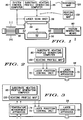
- the LAPCE system includes system control computer 80, substrate heating profile generating computer 85, etching chamber 50 and vacuum generating apparatus 60.
- System control computer 80 is basically a computer capable of controlling the overall functioning of the LAPCE system, for example gas flow, vacuum, and the sequencing of all such system operations.
- Control computer 80 can be a general purpose digital computer with software programmed for LAPCE system control functionality or alternatively the functionality of control computer 80 can be effected by a dedicated hardware implementation or any combination of hardware and software that provide the desired functionality.
- Substrate heating profile generating computer 85 is a computer capable of converting a thickness profile map 120 of semiconductor substrate 40 into a heating profile map 130 of substrate 40. Thickness profile map 120 is generated from thickness and location or position data measured for each portion of a plurality of portions of semiconductor substrate 40. Stand-alone thickness measurement and thickness profile generating systems are commercially available. Therefore, it is possible to provide thickness profile map 120 of substrate 40 to heating profile generating computer 85 from such a stand-alone system. Alternatively, the LAPCE system can comprise the functionality of such thickness and position measurement.
- each portion of semiconductor substrate 40 measured, and subsequently differentially heated can be very small. Typically, this size is much smaller than the size obtainable by employing a spatially confined plasma.
- heating profile map 130 identifies an amount of heating that each portion of semiconductor substrate 40 requires.
- Etching chamber 50 is configured to contain a downstream plasma. As is well known to those skilled in the art, downstream plasma etching is widely regarded as the least damaging of the dry etching technologies, thus providing for potentially the highest quality final layers.
- a carrier gas, containing a reactive chemical or mixture of reactive chemicals is passed through reactive species generating means 56, for example a microwave cavity, and the carrier gas containing the reactive species is directed into etching chamber 50 through inlet port 53. It is well understood that the choice of a reactive chemical, or mixture of reactive chemicals, is determined by the nature of the semiconductor material to be etched. For example a mixture of carbon tetrafluoride (CF 4 ) and oxygen is suitable for etching silicon.
- CF 4 carbon tetrafluoride
- Etching chamber 50 further includes transparent window 54 forming one wall or a portion of a wall of etching chamber 50.
- Substrate 40 is positioned on temperature controlled chuck 52 which is used to maintain substrate 40 at a predetermined temperature. This enables one to maximize the differential heating and overall etch rate of substrate 40.
- Transparent window 54 is positioned so that semiconductor substrate 40 is in a direct line of sight to a laser scan unit 58, shown mounted externally to etching chamber 50 in FIG. 1.
- Laser scan unit 58 is capable of directing an optical heating beam through transparent window 54 to portions of semiconductor substrate 40.
- Laser scan unit 58 is able to scan essentially the entire semiconductor substrate 40 and selectively heat particular portions of semiconductor substrate 40, as per heating profile map 130.
- Etching chamber 50 further comprises outlet port 55 which is coupled to vacuum generating apparatus 60 which serves to maintain etching chamber 50 at a sub-atmospheric pressure. This is consistent with well known downstream plasma etching processing.
- etch chamber 50 may be varied for particular applications.
- the position and nature of reactive species generation means 56, inlet port 53, outlet port 55 and other particulars of etching chamber 50 are individually configurable. Therefore the configuration of the aforementioned non-essential elements is not critical, in general, to the proper functioning of the present invention.
- the relative position of transparent window 54 must allow direct line of sight between semiconductor substrate 40 and laser scan unit 58.
- LAPCE etching chamber 50 will encompass no mechanical motion within the etching chamber during processing thus eliminating this major potential source of contamination.
- the LAPCE system is capable of etching all portions of substrate 40 at all times, thus providing an increased throughput as compared to systems utilizing a spatially confined plasma.
- laser scan unit 58 comprises heating apparatus 70 and position control unit 72.
- Heating apparatus 70 can comprise any high energy optical source capable of being focused to and absorbed by all portions of substrate 40, through transparent window 54 (see FIG. 1).
- heating apparatus 70 must be capable of having its energy output modulated to generate differential heating.
- a laser is well known as such a heating apparatus. Therefore for ease of description and understanding, heating apparatus 70 will heretofore be referred to as laser generation apparatus 70, although it should be understood that other heating elements capable of such energy output modulation can be used.
- position control unit 72 will be understood to be a combination of a computer and mechanical components configured in a manner to be capable of directing the position of any high energy optical source, but for ease of description and understanding will be referred to heretofore as laser position control unit 72.
- laser position control unit 72 The scope of the present invention is not intended to be limited by the use of this laser terminology, and heating sources other than lasers are understood to be included.
- Laser position control unit 72 is capable of moving the position of the output of laser generation apparatus 70 to each of a plurality of portions of a major surface of semiconductor substrate 40 (see FIG. 1), thus differentially heating localized portions of substrate 40 (see FIG. 1). In effecting this movement, laser position control unit 72 utilizes a heating profile map 130 generated by heating profile generating computer 85 and can further effect the modulation of both the energy output from laser generation apparatus 70, and the dwell time for each portion of the major surface of semiconductor substrate 40 (see FIG. 1) in accordance with the thickness of portions thereof as detailed by profile map 130.
- laser scan unit 58 comprises laser generation apparatus 70, laser position control unit 72 as described above with regard to FIG. 2, and temperature measurement apparatus 74.
- temperature measurement apparatus 74 functions to perform dynamic temperature measurements of each portion of the major surface of substrate 40 through transparent window 54 (see FIG. 1).
- measurement apparatus 74 will be understood to comprise a combination of a computer and mechanical components configured in a manner to be capable measuring a temperature of each portion of the major surface of substrate 40 (see FIG. 1), for example by infrared thermography.
- These dynamic temperature measurements provide feedback to heating profile generating computer 85 allowing dynamic updating of heating profile map 130.
- Laser position control unit 72 then utilizes updated heating profile map 130 thus enhancing control of the differential heating and of the resulting etch rates such that a substrate of a predetermined thickness with uniformity enhanced with respect to that of the embodiment described above and in FIG. 2, is obtained.
- laser scan unit 58 comprises laser generation apparatus 70, laser position control unit 72, temperature measurement apparatus 74, thickness measurement apparatus 76 and etch rate computational computer 78.
- Laser generation apparatus 70, position control unit 72 and temperature measurement apparatus 74 are to be understood as described above and in FIGs. 2 and 3.
- thickness measurement apparatus 76 functions to perform dynamic thickness measurements.
- Thickness measurement apparatus 76 can comprise an optical measuring unit, such as a laser interferometer, coupled to a combination of computational and mechanical components configured to allow an initial thickness measurement and subsequent thickness measurements to be made at each portion of the major surface of substrate 40 (see FIG. 1) during etching.
- Feedback of thickness measurements for each portion scanned is directed to etch rate computational computer 78 where an etch rate for each portion of the major surface semiconductor substrate 40 is calculated.
- Etch rate computational computer 78 comprises a computer capable of performing dynamic etch rate calculations. This dynamic etch rate data is directed to heating profile generation computer 85 to allow dynamic updating of heating profile map 130.
- Laser position control unit 72 then utilizes updated heating profile map 130 thus enhancing control of the differential heating and etching for each of the plurality of portions to provide enhanced control of the etch rate for each portion such that an extremely uniform substrate of a predetermined thickness can be obtained.
- temperature measurement apparatus 74 is represented as an optional functioning unit. As one skilled in the art will realize, temperature measurement apparatus 74 can be employed, in the manner of the embodiment associated with FIG. 3, in conjunction and in addition to thickness measurement apparatus 76 to provide additional data and further enhance control of etch rates.
- FIG. 5 A portion of an exemplary semiconductor substrate 40 is illustrated in FIG. 5.
- Semiconductor substrate 40 is composed of handle wafer 10, dielectric layer 20 overlying handle wafer 10, and device wafer 30 overlying dielectric layer 20.
- device wafer 30 is single crystal silicon having an initial thickness on the order of about 200 to 500 ⁇ m.
- Dielectric layer 20 is silicon dioxide and handle wafer 10 is a silicon wafer.
- a typical TTV for such a bonded device wafer 30 would be approximately 10 ⁇ m, but values as high as 50 ⁇ m are not unusual.
- This thickness variation is represented in FIG.5 by the non-parallel representations of major surface 32 and lower surface 34 of device wafer 30 and first thickness 36 and second thickness 38.
- device wafer 30 could have a TTV of approximately 10 ⁇ m where first thickness 36 is, for example 40 ⁇ m and second thickness 38 is, for example 50 ⁇ m. It will be understood by one skilled in the art, that if thickness 36 represents a first portion 36, and thickness 38 a second portion 38 of a plurality of portions, that during the LAPCE process, second portion 38 would be differentially heated to produce a higher etch rate than first portion 36. This differential heating will be maintained until the thickness of the two portions is equal, thus providing an extremely uniform film thickness.
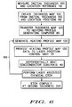
- FIG. 6 is a block diagram representative of the Laser Assisted Plasma Chemical Etch process (LAPCE).
- Initial thickness 100 is measured at each of a plurality of portions of major surface 32 of device wafer 30 (see FIG. 5) and a thickness profile map 120 comprised of thickness and location data is created therefrom. While initial thickness 100 may be measured on a full thickness device wafer 30 (see FIG. 5), typically a preliminary thinning step, such as mechanical grinding or chemical-mechanical polishing, is performed to bring device wafer 30 (see FIG. 5) to a initial thickness 100 close to a predetermined final thickness 200.
- Initial thickness 100 of device wafer 30 can be measured at each of a plurality of portions of a major surface of device wafer 30 (see FIG.
- a location reference 110 is also generated.
- a initial thickness 100 and location reference 110 is generated for each of the plurality of portions of the major surface of device wafer 30 and thickness profile map 120 is generated therefrom.
- thickness profile map 120 is created, it is transferred to heating profile generating computer 85 where heating profile map 130, which is used to control laser position control unit 72, is generated therefrom.
- heating profile map 130 which is used to control laser position control unit 72, is generated therefrom.
- FIGs. 3 and 4 are dynamically controlled etching processes. Each embodiment requires the dynamic updating of heating profile map 130. Therefore, referring again to FIG. 6, arrow 150 represents the repetitive feedback and recalculation of heating profile map 130 that comprises such dynamically controlled process as previously described.
- the present invention provides both an apparatus and method for thinning a semiconductor substrate 40 (see FIG. 1) with a dynamic feedback loop that can provide extremely uniform, thin high quality semiconductor layers.
- improvements in both ultimate thickness control, TTV and surface quality can be obtained.
- prior art etch technology the removal of mechanical motion from within the process chamber during etching, dynamic updating of heating profile maps and the use of low damage downstream etching all contribute to higher quality and process control.
- the ability to etch the entire wafer at all times, as opposed to the scanning confined plasma of prior art etch technology provides for improved throughput and resulting lower costs.
- the ability to define extremely small portions of a surface as compared to prior art etch technology, allow for significant improvements in film uniformity without sacrificing throughput or layer surface quality.
Landscapes
- Drying Of Semiconductors (AREA)
- Lasers (AREA)
- ing And Chemical Polishing (AREA)
Applications Claiming Priority (2)
| Application Number | Priority Date | Filing Date | Title |
|---|---|---|---|
| US432556 | 1995-05-01 | ||
| US08/432,556 US5795493A (en) | 1995-05-01 | 1995-05-01 | Laser assisted plasma chemical etching method |
Publications (2)
| Publication Number | Publication Date |
|---|---|
| EP0741406A2 true EP0741406A2 (de) | 1996-11-06 |
| EP0741406A3 EP0741406A3 (de) | 1999-01-13 |
Family
ID=23716652
Family Applications (1)
| Application Number | Title | Priority Date | Filing Date |
|---|---|---|---|
| EP96106731A Withdrawn EP0741406A3 (de) | 1995-05-01 | 1996-04-29 | Vorrichtung und Verfahren zum laserunterstützten chemischen Plasmaätzen |
Country Status (3)
| Country | Link |
|---|---|
| US (1) | US5795493A (de) |
| EP (1) | EP0741406A3 (de) |
| JP (1) | JPH08306673A (de) |
Cited By (12)
| Publication number | Priority date | Publication date | Assignee | Title |
|---|---|---|---|---|
| WO1998044541A1 (en) * | 1997-04-03 | 1998-10-08 | Memc Electronic Materials, Inc. | Flattening process for semiconductor wafers |
| WO1998044549A1 (en) * | 1997-04-03 | 1998-10-08 | Memc Electronic Materials, Inc. | Flattening process for epitaxial semiconductor wafers |
| US6030887A (en) * | 1998-02-26 | 2000-02-29 | Memc Electronic Materials, Inc. | Flattening process for epitaxial semiconductor wafers |
| FR2788374A1 (fr) * | 1998-12-02 | 2000-07-13 | Mitsubishi Electric Corp | Procede de fabrication d'un dispositif a semiconducteur du type soi |
| EP1071116A1 (de) * | 1999-07-21 | 2001-01-24 | Applied Materials, Inc. | Verfahren und Vorrichtung zur Entfernung eines Materials von der Peripherie eines Substrats, mittels einer entfernte Plasmaquelle |
| US6200908B1 (en) | 1999-08-04 | 2001-03-13 | Memc Electronic Materials, Inc. | Process for reducing waviness in semiconductor wafers |
| WO2002012585A3 (en) * | 2000-08-08 | 2002-04-18 | Tokyo Electron Ltd | Processing apparatus and cleaning method |
| DE10137570A1 (de) * | 2001-07-30 | 2003-02-27 | Infineon Technologies Ag | Verfahren und Vorrichtung zur Herstellung mindestens einer Vertiefung in einem Halbleitermaterial |
| WO2004077505A3 (en) * | 2003-02-27 | 2005-03-31 | Lam Res Corp | Critical dimension variation compensation across a wafer by means of local wafer temperature control |
| WO2005067009A3 (en) * | 2003-12-24 | 2005-08-18 | Lam Res Corp | Process controls for improved wafer uniformity using integrated or standalone metrology |
| US20200075351A1 (en) * | 2018-09-04 | 2020-03-05 | Tokyo Electron Limited | Processing systems and platforms for roughness reduction of materials using illuminated etch solutions |
| WO2026005894A1 (en) * | 2024-06-24 | 2026-01-02 | Applied Materials, Inc. | Substrate processing for improved wafer thickness uniformity |
Families Citing this family (33)
| Publication number | Priority date | Publication date | Assignee | Title |
|---|---|---|---|---|
| US5891744A (en) * | 1996-01-29 | 1999-04-06 | Micron Technology, Inc. | Method of monitoring a process of manufacturing a semiconductor wafer including hemispherical grain polysilicon |
| JP3917703B2 (ja) * | 1997-02-18 | 2007-05-23 | スピードファム株式会社 | プラズマエッチング方法及びその装置 |
| US6632321B2 (en) * | 1998-01-06 | 2003-10-14 | Applied Materials, Inc | Method and apparatus for monitoring and controlling wafer fabrication process |
| JP2000036488A (ja) * | 1998-07-21 | 2000-02-02 | Speedfam-Ipec Co Ltd | ウエハ平坦化方法及びそのシステム |
| US5953578A (en) * | 1998-09-08 | 1999-09-14 | Winbond Electronics Corp. | Global planarization method using plasma etching |
| US8080380B2 (en) | 1999-05-21 | 2011-12-20 | Illumina, Inc. | Use of microfluidic systems in the detection of target analytes using microsphere arrays |
| US8481268B2 (en) | 1999-05-21 | 2013-07-09 | Illumina, Inc. | Use of microfluidic systems in the detection of target analytes using microsphere arrays |
| US7510664B2 (en) | 2001-01-30 | 2009-03-31 | Rapt Industries, Inc. | Apparatus and method for atmospheric pressure reactive atom plasma processing for shaping of damage free surfaces |
| US7591957B2 (en) * | 2001-01-30 | 2009-09-22 | Rapt Industries, Inc. | Method for atmospheric pressure reactive atom plasma processing for surface modification |
| DE10296328B4 (de) * | 2001-02-14 | 2010-04-08 | Advanced Micro Devices, Inc., Sunnyvale | Prozesslinie und Verfahren zum Steuern eines Ätzprozesses |
| US6746616B1 (en) * | 2001-03-27 | 2004-06-08 | Advanced Micro Devices, Inc. | Method and apparatus for providing etch uniformity using zoned temperature control |
| US6660177B2 (en) | 2001-11-07 | 2003-12-09 | Rapt Industries Inc. | Apparatus and method for reactive atom plasma processing for material deposition |
| US6500681B1 (en) * | 2002-01-11 | 2002-12-31 | Advanced Micro Devices, Inc. | Run-to-run etch control by feeding forward measured metal thickness |
| US6936182B2 (en) * | 2002-02-28 | 2005-08-30 | The Regents Of The University Of California | Method and system for optical figuring by imagewise heating of a solvent |
| US20070066076A1 (en) * | 2005-09-19 | 2007-03-22 | Bailey Joel B | Substrate processing method and apparatus using a combustion flame |
| US20040110314A1 (en) * | 2002-12-05 | 2004-06-10 | Ravi Kramadhati V. | Silicon-on-insulator devices and methods for fabricating the same |
| US7371992B2 (en) | 2003-03-07 | 2008-05-13 | Rapt Industries, Inc. | Method for non-contact cleaning of a surface |
| DE10328559B4 (de) * | 2003-06-24 | 2006-04-20 | Leibniz-Institut für Oberflächenmodifizierung e.V. | Verfahren zur Präzisionsbearbeitung von transparenten Materialien mit gepulster Laserstrahlung |
| US7304263B2 (en) * | 2003-08-14 | 2007-12-04 | Rapt Industries, Inc. | Systems and methods utilizing an aperture with a reactive atom plasma torch |
| US7297892B2 (en) * | 2003-08-14 | 2007-11-20 | Rapt Industries, Inc. | Systems and methods for laser-assisted plasma processing |
| CN100406197C (zh) * | 2006-07-17 | 2008-07-30 | 哈尔滨工业大学 | 常压等离子体抛光装置 |
| JP4919860B2 (ja) * | 2007-03-30 | 2012-04-18 | 東京エレクトロン株式会社 | ガス分析装置及び基板処理装置 |
| CN100462199C (zh) * | 2007-04-11 | 2009-02-18 | 哈尔滨工业大学 | 常压等离子体抛光方法 |
| WO2012103054A1 (en) * | 2011-01-25 | 2012-08-02 | The Board Of Trustees Of The University Of Illinois | Method of selectively etching a three-dimensional structure |
| JP5995411B2 (ja) * | 2011-04-28 | 2016-09-21 | キヤノン株式会社 | 半導体ウェハーの製造方法、レンズの製造方法およびミラーの製造方法 |
| FR3002687B1 (fr) * | 2013-02-26 | 2015-03-06 | Soitec Silicon On Insulator | Procede de traitement d une structure |
| US10226852B2 (en) * | 2013-12-31 | 2019-03-12 | Nova Measuring Instruments Ltd. | Surface planarization system and method |
| US10978321B2 (en) | 2015-12-31 | 2021-04-13 | Nova Measuring Instruments Ltd. | Method and system for processing patterned structures |
| JP6861817B2 (ja) | 2016-12-14 | 2021-04-21 | マトソン テクノロジー インコーポレイテッドMattson Technology, Inc. | 急速熱活性化プロセスと連係した、プラズマを使用する原子層エッチングプロセス |
| JP7383339B2 (ja) * | 2019-10-16 | 2023-11-20 | 株式会社ディスコ | 被加工物の加工方法及び加工装置 |
| US12046477B2 (en) * | 2021-01-08 | 2024-07-23 | Taiwan Semiconductor Manufacturing Company, Ltd. | By-site-compensated etch back for local planarization/topography adjustment |
| US12004307B2 (en) | 2021-06-09 | 2024-06-04 | International Business Machines Corporation | Short or near short etch rework |
| US12243745B2 (en) | 2022-02-07 | 2025-03-04 | Taiwan Semiconductor Manufacturing Co., Ltd. | Dynamic laser-assisted etching |
Family Cites Families (7)
| Publication number | Priority date | Publication date | Assignee | Title |
|---|---|---|---|---|
| EP0418540A3 (en) * | 1989-08-11 | 1991-08-07 | Sanyo Electric Co., Ltd. | Dry etching method |
| JPH0834198B2 (ja) * | 1990-11-28 | 1996-03-29 | 信越半導体株式会社 | Soi基板における単結晶薄膜層の膜厚制御方法 |
| JPH0817166B2 (ja) * | 1991-04-27 | 1996-02-21 | 信越半導体株式会社 | 超薄膜soi基板の製造方法及び製造装置 |
| US5254830A (en) * | 1991-05-07 | 1993-10-19 | Hughes Aircraft Company | System for removing material from semiconductor wafers using a contained plasma |
| US5376224A (en) * | 1992-02-27 | 1994-12-27 | Hughes Aircraft Company | Method and apparatus for non-contact plasma polishing and smoothing of uniformly thinned substrates |
| JPH06140365A (ja) * | 1992-10-23 | 1994-05-20 | Shin Etsu Handotai Co Ltd | Soi基板におけるsoi膜厚均一化方法 |
| US5375064A (en) * | 1993-12-02 | 1994-12-20 | Hughes Aircraft Company | Method and apparatus for moving a material removal tool with low tool accelerations |
-
1995
- 1995-05-01 US US08/432,556 patent/US5795493A/en not_active Expired - Fee Related
-
1996
- 1996-04-25 JP JP8127647A patent/JPH08306673A/ja active Pending
- 1996-04-29 EP EP96106731A patent/EP0741406A3/de not_active Withdrawn
Cited By (16)
| Publication number | Priority date | Publication date | Assignee | Title |
|---|---|---|---|---|
| WO1998044549A1 (en) * | 1997-04-03 | 1998-10-08 | Memc Electronic Materials, Inc. | Flattening process for epitaxial semiconductor wafers |
| WO1998044541A1 (en) * | 1997-04-03 | 1998-10-08 | Memc Electronic Materials, Inc. | Flattening process for semiconductor wafers |
| US6030887A (en) * | 1998-02-26 | 2000-02-29 | Memc Electronic Materials, Inc. | Flattening process for epitaxial semiconductor wafers |
| FR2788374A1 (fr) * | 1998-12-02 | 2000-07-13 | Mitsubishi Electric Corp | Procede de fabrication d'un dispositif a semiconducteur du type soi |
| US6436303B1 (en) | 1999-07-21 | 2002-08-20 | Applied Materials, Inc. | Film removal employing a remote plasma source |
| EP1071116A1 (de) * | 1999-07-21 | 2001-01-24 | Applied Materials, Inc. | Verfahren und Vorrichtung zur Entfernung eines Materials von der Peripherie eines Substrats, mittels einer entfernte Plasmaquelle |
| US6200908B1 (en) | 1999-08-04 | 2001-03-13 | Memc Electronic Materials, Inc. | Process for reducing waviness in semiconductor wafers |
| US7201174B2 (en) | 2000-08-08 | 2007-04-10 | Tokyo Electron Limited | Processing apparatus and cleaning method |
| WO2002012585A3 (en) * | 2000-08-08 | 2002-04-18 | Tokyo Electron Ltd | Processing apparatus and cleaning method |
| DE10137570A1 (de) * | 2001-07-30 | 2003-02-27 | Infineon Technologies Ag | Verfahren und Vorrichtung zur Herstellung mindestens einer Vertiefung in einem Halbleitermaterial |
| WO2004077505A3 (en) * | 2003-02-27 | 2005-03-31 | Lam Res Corp | Critical dimension variation compensation across a wafer by means of local wafer temperature control |
| WO2005067009A3 (en) * | 2003-12-24 | 2005-08-18 | Lam Res Corp | Process controls for improved wafer uniformity using integrated or standalone metrology |
| US7018855B2 (en) | 2003-12-24 | 2006-03-28 | Lam Research Corporation | Process controls for improved wafer uniformity using integrated or standalone metrology |
| US20200075351A1 (en) * | 2018-09-04 | 2020-03-05 | Tokyo Electron Limited | Processing systems and platforms for roughness reduction of materials using illuminated etch solutions |
| US12112959B2 (en) * | 2018-09-04 | 2024-10-08 | Tokyo Electron Limited | Processing systems and platforms for roughness reduction of materials using illuminated etch solutions |
| WO2026005894A1 (en) * | 2024-06-24 | 2026-01-02 | Applied Materials, Inc. | Substrate processing for improved wafer thickness uniformity |
Also Published As
| Publication number | Publication date |
|---|---|
| JPH08306673A (ja) | 1996-11-22 |
| EP0741406A3 (de) | 1999-01-13 |
| US5795493A (en) | 1998-08-18 |
Similar Documents
| Publication | Publication Date | Title |
|---|---|---|
| US5795493A (en) | Laser assisted plasma chemical etching method | |
| EP0514046B1 (de) | Einrichtung und Verfahren zur Kontrolle und Durchführung der Ätzung eines Wafers | |
| US6514838B2 (en) | Method for non mass selected ion implant profile control | |
| US6321134B1 (en) | Clustertool system software using plasma immersion ion implantation | |
| US5002631A (en) | Plasma etching apparatus and method | |
| KR100999002B1 (ko) | 반도체 웨이퍼 처리 방법 및 장치 | |
| EP0511777B1 (de) | Verfahren und Vorrichtung zur Herstellung einer extrem dünnen monokristallinen Siliziumschicht bei einem SOI Substrat mittels einer durch Interferometrie kontrollierten Ätzmethode | |
| US8858753B2 (en) | Focus ring heating method, plasma etching apparatus, and plasma etching method | |
| JPH04196559A (ja) | Soi基板における単結晶薄膜層の膜厚制御方法 | |
| JPH1031039A (ja) | 計測装置および計測方法 | |
| JPH10313128A (ja) | シリコン基板の異方性エッチング方法及び太陽電池の製造方法 | |
| US4784963A (en) | Method for light-induced photolytic deposition simultaneously independently controlling at least two different frequency radiations during the process | |
| US5170098A (en) | Plasma processing method and apparatus for use in carrying out the same | |
| JP2000256094A (ja) | シリコンエピタキシャル成長ウェーハ製造方法およびその装置 | |
| EP0968081A1 (de) | Planarisierungsprozess für verbundene halbleitersubstrate | |
| GB2087315A (en) | Plasma etching of aluminium | |
| JPS58165330A (ja) | 半導体装置の製造方法 | |
| JP2663923B2 (ja) | Soi基板の製造方法 | |
| JP2970217B2 (ja) | Soi基板におけるsoi膜厚均一化方法 | |
| JPH10300912A (ja) | 回折格子用基板 | |
| JPH02278720A (ja) | プラズマドーピング装置 | |
| US12249489B2 (en) | Optical device improvement | |
| JPH08316208A (ja) | ラジカル反応を用いた加工装置および加工方法 | |
| JPS60162776A (ja) | プラズマ処理装置 | |
| Korchnoi et al. | Silicon Trenching Using Dry Etch Process for Backside FIB and Probing |
Legal Events
| Date | Code | Title | Description |
|---|---|---|---|
| PUAI | Public reference made under article 153(3) epc to a published international application that has entered the european phase |
Free format text: ORIGINAL CODE: 0009012 |
|
| AK | Designated contracting states |
Kind code of ref document: A2 Designated state(s): DE FR GB NL |
|
| PUAL | Search report despatched |
Free format text: ORIGINAL CODE: 0009013 |
|
| RHK1 | Main classification (correction) |
Ipc: H01L 21/3065 |
|
| AK | Designated contracting states |
Kind code of ref document: A3 Designated state(s): DE FR GB NL |
|
| STAA | Information on the status of an ep patent application or granted ep patent |
Free format text: STATUS: THE APPLICATION IS DEEMED TO BE WITHDRAWN |
|
| 18D | Application deemed to be withdrawn |
Effective date: 19990714 |