EP0742553A2 - System und Verfahren für Laserrückkopplung eines optischen Speichers - Google Patents
System und Verfahren für Laserrückkopplung eines optischen Speichers Download PDFInfo
- Publication number
- EP0742553A2 EP0742553A2 EP96106699A EP96106699A EP0742553A2 EP 0742553 A2 EP0742553 A2 EP 0742553A2 EP 96106699 A EP96106699 A EP 96106699A EP 96106699 A EP96106699 A EP 96106699A EP 0742553 A2 EP0742553 A2 EP 0742553A2
- Authority
- EP
- European Patent Office
- Prior art keywords
- laser
- gain
- feedback system
- gain value
- oscillating
- Prior art date
- Legal status (The legal status is an assumption and is not a legal conclusion. Google has not performed a legal analysis and makes no representation as to the accuracy of the status listed.)
- Granted
Links
Images


Classifications
-
- G—PHYSICS
- G11—INFORMATION STORAGE
- G11B—INFORMATION STORAGE BASED ON RELATIVE MOVEMENT BETWEEN RECORD CARRIER AND TRANSDUCER
- G11B7/00—Recording or reproducing by optical means, e.g. recording using a thermal beam of optical radiation by modifying optical properties or the physical structure, reproducing using an optical beam at lower power by sensing optical properties; Record carriers therefor
- G11B7/12—Heads, e.g. forming of the optical beam spot or modulation of the optical beam
- G11B7/125—Optical beam sources therefor, e.g. laser control circuitry specially adapted for optical storage devices; Modulators, e.g. means for controlling the size or intensity of optical spots or optical traces
- G11B7/126—Circuits, methods or arrangements for laser control or stabilisation
Definitions
- the present invention relates to a method and a system for controlling the laser feedback of an optical memory system.
- a feedback system is used to adjust the amount of light irradiated by, for example, a laser diode onto an optical disk. If the amount of light irradiated onto an optical disk is too low, the S/N ratio (signal-to-noise ratio) of the resulting signal deteriorates, so that the detection of the digital information becomes complicated. On the other hand, if the amount of light irradiated by the laser diode onto the disk is too high, the laser feedback system starts oscillating with the result that the optical detection system is not in a stable working condition and that the digital information of the optical memory cannot be obtained.
- the optimum amount of light i.e. the most suitable feedback gain value
- the laser feedback gain value is set manually to its suitable value depending on the disk used.
- the operation of manually setting the gain value is a difficult task, because the laser feedback gain value is set to be maximum by observing the eye-pattern, so that the system as a whole does not oscillate.
- the laser feedback system of an optical memory comprises a laser means for generating a laser beam irradiating the optical memory means, a detection means for detecting the light emanating from the optical memory means, an oscillation detecting means connected to the detection means, a gain controlling means connected to the oscillation detecting means, and a multiplying means connected to the detection means and controlled by the gain controlling means, wherein the gain of the laser means set by the multiplying means is controlled by the gain controlling means.
- the laser means of the laser feedback system can be a laser diode.
- the detecting means of the laser feedback system can be a photodiode.
- the laser means of the laser feedback system is driven by a laser driving means which is connected to the multiplying means.
- the oscillation detecting means of the laser feedback system comprises an envelope detector, a sampling/holder and a comparator.
- the gain controlling system of the laser feedback system comprises a counter controller, a counter and a D/A converter.
- the counter and the sampling/holder circuit of the laser feedback system are operated simultaneously by the signal of a clock oscillator.
- the method for operating a laser feedback system of an optical memory means wherein the light emanated from the optical memory means, which is irradiated by a laser means, is fed back to the laser means, the feedback system comprises an oscillation detecting means which detects if the feedback system is oscillating or not, and wherein an optimum gain of the laser means is achieved with an iterative method using the information of the oscillating detection means whether the feedback system is oscillating or not.
- the feedback system starts with a predetermined gain value, upon detection of a non-oscillating state of the feedback system the gain of the laser means is gradually increased, and upon detection of an oscillating state of the feedback system the gain is gradually decreased.
- the method starts with a gain value so small that the system will not oscillate.
- the gain value is gradually increased by a first predetermined amount as long as the oscillation detecting means does not detect an oscillating state of the feedback system, the gain value is decreased by a second predetermined amount when the oscillation detecting means detects an oscillation state of the feedback system, and then the resulting gain value is latched.
- the first and second predetermined amounts are equal.
- the first and second predetermined amounts can be set externally.
- the Fig. 1 shows a block diagram for the principle explanation of an automatic gain control (AGC) for a laser feedback system used in connection with an optical memory like an optical disk.
- a laser diode 2 generates a laser beam which irradiates the surface of an optical disk 1.
- the basic feedback system consists of a photodiode 3 which receives the reflected light from the disk 1.
- the resulting signal is inputted parallel to an oscillation detector 4 and to a multiplier 6.
- the output of the multiplier 6 is inputted to a laser driver 7, which drives the laser diode 2.
- the oscillation detector 4 detects whether the feedback system oscillates or not and generates an output signal which is inputted to a gain controller 5.
- the output signal of the oscillation detector 4 basically consists of three information items, namely no oscillation occurs, feedback oscillation does occur, and to latch the present gain.
- the gain controller 4 controls the gain value of the multiplier 6 in the following way. If the information signal contains the information that no oscillation of the feedback system occurs, the gain of the multiplier is increased by a predetermined amount. The resulting signal of the multiplier 6 is fed to a laser driver 7 which drives the laser diode 2. According to the increase in gain the laser diode generates more light. This increase in gain is continued step by step until the oscillation detector 4 detects the presence of oscillations in the feedback system. Then the gain controller 5 receives the information that oscillations do occur and decreases the gain of the multiplier 6 by a predetermined amount. Thereby the amount of decrease in gain can differ from the amount of increase in gain of the first part of the iteration.
- the laser diode now generates less light than in the previous step. If the amount of increase and decrease are the same or the amount of decrease is larger than the amount of increase, then the feedback system is now after this one decrease step B in a stable, non-oscillating state.
- the feedback system further comprises lenses 3, 8 and 10, beamsplitters 9 and 11, and an amplifier 13 for the amplification of the photodiode signal.
- Fig. 2 shows the photo detector signal S versus the amplifier gain G, where the photo detector signal S is standardized to the laser light intensity. Therefore at low amplifier gain G the standardized signal is large but involves a low S/N ratio.
- the minimum photo detector signal S on the left side of the figure the system is in a non-oscillating normal detected signal area (left hand side of Fig. 2 with the reference sign "N-O").
- N-O normal detected signal area
- Fig. 3 shows in principle the same curve as Fig. 2 but indicating different areas A, B, C to explain the method of iteration for obtaining a suitable maximum gain.
- the multiplier gain is so small that photodiode signal S does not oscillate, which is depicted in the area A in Fig. 3.
- the gain controller generates a multiplier gain G.
- the gain controller increases the multiplier gain G little by little. This means in Fig. 3 that the actual photosignal value (a point on the curve) is moving from area A on the curve to area B.
- the oscillation detector detects that the photodiode signal, i.e.
- the whole feedback system oscillates. This takes place in the area C in Fig. 3.
- the gain controller gets the signal from the oscillation detector that the photodiode signal oscillates the gain controller sets the multiplier gain G one step smaller than the present gain, that means it resets the gain value to the preceding gain value, if the increasing and decreasing steps are of the same value. Therefore the multiplier gain is set at area B in Fig. 3.
- This area B is the suitable maximum gain area and therefore the multiplier gain is set to be constant at this suitable maximum gain area so that the photodiode signal does not oscillate.
- the oscillation detector compares the photodiode signal S(G), where G is the actual (present) gain value, with the photodiode signal S(G'), where G' is the preceding gain value (i.e. just one step before present G). Then the oscillation detector generates the digital information signal. This signal indicates whether the photodiode signal oscillates or not. If S(G) is smaller than S(G'), then G is in normal detected signal area of Fig. 3. The oscillation detector sends the signal, that the photodiode signal does not oscillate, to the gain controller. Then the gain controller sets the gain at the multiplier one step larger.
- the gain controller After iterating this suitable maximum gain signal G the gain controller latches the thus obtained gain value for future use on this particular type of disks. It is also possible to run this iteration every time when a disk is changed.
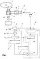
- Fig. 4 shows a more detailed block diagram of an automatic gain control for laser feedback systems. Means having same functions as the means of the embodiment of fig. 1 are marked with same reference numbers.
- the laser diode 2 emits light which passes the lens 8, the multi-purpose beamsplitter 9 and is focussed by the lens 10 onto the information carrying surface of the optical disk 1.
- the reflected, information carrying light passes again the lens 10 and is reflected on the 45° plane of the multi-purpose beamsplitter 9 in a perpendicular direction.
- the reflected light is split by the use of a second beamsplitter 11 into one beam which is directed to an optical detecting system for detecting the phase pit signals (not shown in the figure), i.e. for detecting the information and in a second beam which passes the beamsplitter 11 and the further lens 12 and is incident upon a photodiode 3.
- the signal of the photodiode 3 is usually amplified by the amplifier 13 and is outputted to the multiplier 6 and the oscillation detector 4.
- the oscillation detector 4 consists of an envelope detector 14 which detects the form of the photodiode signal. The resulting signal is then given to a sampling and holding circuit 15, which stores the previous envelope signal, and to a comparator 16 which compares the previous signal with the present signal.
- the output of the comparator 16 is connected to the gain controller 5, which consists of a counter controller 18 followed by a counter 19 and a digital to analog converter 20.
- Both the counter 19 and the sampling and holding circuit 15 are operated simultaneously by the signal of a clock oscillator 17.
- the counter controller 18 increases the counter by one so that the multiplier gain of multiplier 6 is increased. If the comparator 16 outputs that an oscillating state has occurred then the counter controller 18 decreases the counter value of the counter 19 by one so that the gain of the multiplier 6 is decreased by a one step, which results that the system is now again in the stable area B. This value is then latched and used for the optical memory disk used in the system.
Landscapes
- Physics & Mathematics (AREA)
- Optics & Photonics (AREA)
- Semiconductor Lasers (AREA)
- Optical Recording Or Reproduction (AREA)
- Optical Head (AREA)
Applications Claiming Priority (2)
| Application Number | Priority Date | Filing Date | Title |
|---|---|---|---|
| GB9509307A GB2300731A (en) | 1995-05-06 | 1995-05-06 | Control of a laser in an optical memory system |
| GB9509307 | 1995-05-06 |
Publications (3)
| Publication Number | Publication Date |
|---|---|
| EP0742553A2 true EP0742553A2 (de) | 1996-11-13 |
| EP0742553A3 EP0742553A3 (de) | 1997-08-13 |
| EP0742553B1 EP0742553B1 (de) | 1999-08-11 |
Family
ID=10774139
Family Applications (1)
| Application Number | Title | Priority Date | Filing Date |
|---|---|---|---|
| EP96106699A Expired - Lifetime EP0742553B1 (de) | 1995-05-06 | 1996-04-27 | System und Verfahren für Laserrückkopplung eines optischen Speichers |
Country Status (5)
| Country | Link |
|---|---|
| US (1) | US5764614A (de) |
| EP (1) | EP0742553B1 (de) |
| JP (1) | JP3948763B2 (de) |
| DE (1) | DE69603654T2 (de) |
| GB (1) | GB2300731A (de) |
Cited By (2)
| Publication number | Priority date | Publication date | Assignee | Title |
|---|---|---|---|---|
| WO2006051500A3 (en) * | 2004-11-15 | 2006-08-17 | Koninkl Philips Electronics Nv | Optimized gain for optical disc actuator control |
| US10709330B2 (en) | 2004-11-15 | 2020-07-14 | Koninklijke Philips N.V. | Ambulatory medical telemetry device having an audio indicator |
Families Citing this family (1)
| Publication number | Priority date | Publication date | Assignee | Title |
|---|---|---|---|---|
| US7494354B2 (en) * | 2006-07-25 | 2009-02-24 | Hon Hai Precision Ind. Co., Ltd. | Card edge connector with ejector |
Family Cites Families (11)
| Publication number | Priority date | Publication date | Assignee | Title |
|---|---|---|---|---|
| US4516242A (en) * | 1981-06-18 | 1985-05-07 | Tokyo Shibaura Denki Kabushiki Kaisha | Output stabilizing device |
| JPS5883342A (ja) * | 1981-11-13 | 1983-05-19 | Hitachi Ltd | 光学式情報読取装置におけるレ−ザ出力制御装置 |
| DE3546599C2 (de) * | 1984-11-20 | 1993-06-03 | Olympus Optical Co., Ltd., Tokio/Tokyo, Jp | |
| JPH0618422B2 (ja) * | 1987-10-20 | 1994-03-09 | 富士写真フイルム株式会社 | レーザ記録装置 |
| JP2812441B2 (ja) * | 1988-10-11 | 1998-10-22 | キヤノン株式会社 | 光学的情報記録再生装置 |
| JP2682222B2 (ja) * | 1990-10-01 | 1997-11-26 | 三菱電機株式会社 | 情報記憶装置 |
| JPH0595150A (ja) * | 1991-06-28 | 1993-04-16 | Toshiba Corp | レーザ制御回路 |
| JP3075632B2 (ja) * | 1992-02-27 | 2000-08-14 | パイオニア株式会社 | 光ディスクプレーヤ |
| JP3519102B2 (ja) * | 1993-06-08 | 2004-04-12 | パイオニア株式会社 | 光ディスク記録情報再生装置 |
| DE4415508A1 (de) * | 1994-05-03 | 1995-11-09 | Thomson Brandt Gmbh | Abtastgerät mit Adaptation |
| US5602814A (en) * | 1994-10-06 | 1997-02-11 | International Business Machines Corporation | Calibration of write-once disks using a single disk sector |
-
1995
- 1995-05-06 GB GB9509307A patent/GB2300731A/en not_active Withdrawn
-
1996
- 1996-04-27 DE DE69603654T patent/DE69603654T2/de not_active Expired - Fee Related
- 1996-04-27 EP EP96106699A patent/EP0742553B1/de not_active Expired - Lifetime
- 1996-05-03 US US08/655,874 patent/US5764614A/en not_active Expired - Lifetime
- 1996-05-07 JP JP11282896A patent/JP3948763B2/ja not_active Expired - Fee Related
Cited By (2)
| Publication number | Priority date | Publication date | Assignee | Title |
|---|---|---|---|---|
| WO2006051500A3 (en) * | 2004-11-15 | 2006-08-17 | Koninkl Philips Electronics Nv | Optimized gain for optical disc actuator control |
| US10709330B2 (en) | 2004-11-15 | 2020-07-14 | Koninklijke Philips N.V. | Ambulatory medical telemetry device having an audio indicator |
Also Published As
| Publication number | Publication date |
|---|---|
| GB2300731A (en) | 1996-11-13 |
| GB9509307D0 (en) | 1995-06-28 |
| DE69603654T2 (de) | 1999-12-30 |
| JP3948763B2 (ja) | 2007-07-25 |
| DE69603654D1 (de) | 1999-09-16 |
| EP0742553B1 (de) | 1999-08-11 |
| US5764614A (en) | 1998-06-09 |
| EP0742553A3 (de) | 1997-08-13 |
| JPH097177A (ja) | 1997-01-10 |
Similar Documents
| Publication | Publication Date | Title |
|---|---|---|
| US5436880A (en) | Laser power control in an optical recording system using partial correction of reflected signal error | |
| US4516242A (en) | Output stabilizing device | |
| US5029155A (en) | Optical information recording/reproducing apparatus in which recording power is set prior to recording | |
| EP0089021A2 (de) | Gerät zur Verhütung von Doppelaufzeichnen einer optischen Scheibe | |
| US5347124A (en) | Control system for oscillatory-mirror light beam deflector | |
| US5233596A (en) | Optical recording/reproducing apparatus including both automatic power control and temperature-based drive current control | |
| EP0478275A2 (de) | Verfahren und Gerät zur Laserleistungssteuerung in einem optischen Scheiberantriebsgerät | |
| US5764614A (en) | Laser intensity gain control for detecting oscillation in the feedback circuit | |
| US5862111A (en) | Optical disk device which performs auto gain control process on servo signals which perform illuminating control of a light beam on the disk's recording surface | |
| EP1211678B1 (de) | Lightmengen-Steuereinrichtung und damit versehenes Informationsaufzeichnungsgerät | |
| EP0364213B1 (de) | Verfahren und Vorrichtung zum Betreiben der Lichtquelle durch einen gespeicherten Stromwert und zur Erzeugung von Information | |
| JPH01106667A (ja) | レーザ記録装置 | |
| KR100235331B1 (ko) | 최적 기록파워 제어를 위한 광 기록재생 장치 | |
| US5355360A (en) | Semiconductor laser controlling apparatus | |
| US5193083A (en) | Optical pick-up device | |
| EP0436939B1 (de) | Datenwiedergabegerät für optische Platte | |
| US6754156B2 (en) | Recording apparatus for use with optical recording medium and method thereof | |
| US5739521A (en) | Laser diode controlling method and apparatus for compact disk drive | |
| JPH0773496A (ja) | 半導体レーザ装置 | |
| JPH11144287A (ja) | 光ディスク記録装置 | |
| JPH05128571A (ja) | 半導体レーザ駆動装置 | |
| JP3229756B2 (ja) | 光ピックアップ用半導体レーザ装置 | |
| KR100515675B1 (ko) | 정보기록/재생장치의레이저파워제어장치 | |
| JPH1125474A (ja) | 光ディスク装置 | |
| JPH02108248A (ja) | レーザ発光素子の出力制御装置 |
Legal Events
| Date | Code | Title | Description |
|---|---|---|---|
| PUAI | Public reference made under article 153(3) epc to a published international application that has entered the european phase |
Free format text: ORIGINAL CODE: 0009012 |
|
| AK | Designated contracting states |
Kind code of ref document: A2 Designated state(s): DE FR GB IT |
|
| PUAL | Search report despatched |
Free format text: ORIGINAL CODE: 0009013 |
|
| AK | Designated contracting states |
Kind code of ref document: A3 Designated state(s): DE FR GB IT |
|
| 17P | Request for examination filed |
Effective date: 19980116 |
|
| RAP1 | Party data changed (applicant data changed or rights of an application transferred) |
Owner name: THOMSON MULTIMEDIA |
|
| 17Q | First examination report despatched |
Effective date: 19980225 |
|
| GRAG | Despatch of communication of intention to grant |
Free format text: ORIGINAL CODE: EPIDOS AGRA |
|
| GRAG | Despatch of communication of intention to grant |
Free format text: ORIGINAL CODE: EPIDOS AGRA |
|
| GRAH | Despatch of communication of intention to grant a patent |
Free format text: ORIGINAL CODE: EPIDOS IGRA |
|
| GRAH | Despatch of communication of intention to grant a patent |
Free format text: ORIGINAL CODE: EPIDOS IGRA |
|
| GRAA | (expected) grant |
Free format text: ORIGINAL CODE: 0009210 |
|
| AK | Designated contracting states |
Kind code of ref document: B1 Designated state(s): DE FR GB IT |
|
| ITF | It: translation for a ep patent filed | ||
| REF | Corresponds to: |
Ref document number: 69603654 Country of ref document: DE Date of ref document: 19990916 |
|
| ET | Fr: translation filed | ||
| PLBE | No opposition filed within time limit |
Free format text: ORIGINAL CODE: 0009261 |
|
| STAA | Information on the status of an ep patent application or granted ep patent |
Free format text: STATUS: NO OPPOSITION FILED WITHIN TIME LIMIT |
|
| 26N | No opposition filed | ||
| REG | Reference to a national code |
Ref country code: GB Ref legal event code: 746 Effective date: 20010813 |
|
| REG | Reference to a national code |
Ref country code: GB Ref legal event code: IF02 |
|
| REG | Reference to a national code |
Ref country code: FR Ref legal event code: D6 |
|
| PGFP | Annual fee paid to national office [announced via postgrant information from national office to epo] |
Ref country code: IT Payment date: 20080424 Year of fee payment: 13 |
|
| PGFP | Annual fee paid to national office [announced via postgrant information from national office to epo] |
Ref country code: GB Payment date: 20090330 Year of fee payment: 14 |
|
| PGFP | Annual fee paid to national office [announced via postgrant information from national office to epo] |
Ref country code: FR Payment date: 20090423 Year of fee payment: 14 Ref country code: DE Payment date: 20090423 Year of fee payment: 14 |
|
| GBPC | Gb: european patent ceased through non-payment of renewal fee |
Effective date: 20100427 |
|
| REG | Reference to a national code |
Ref country code: FR Ref legal event code: ST Effective date: 20101230 |
|
| PG25 | Lapsed in a contracting state [announced via postgrant information from national office to epo] |
Ref country code: DE Free format text: LAPSE BECAUSE OF NON-PAYMENT OF DUE FEES Effective date: 20101103 |
|
| PG25 | Lapsed in a contracting state [announced via postgrant information from national office to epo] |
Ref country code: IT Free format text: LAPSE BECAUSE OF NON-PAYMENT OF DUE FEES Effective date: 20090427 Ref country code: GB Free format text: LAPSE BECAUSE OF NON-PAYMENT OF DUE FEES Effective date: 20100427 |
|
| PG25 | Lapsed in a contracting state [announced via postgrant information from national office to epo] |
Ref country code: FR Free format text: LAPSE BECAUSE OF NON-PAYMENT OF DUE FEES Effective date: 20100430 |