EP0742602A2 - Monolithischer multifunktioneller balancierter Schalter und Phasenschieber - Google Patents
Monolithischer multifunktioneller balancierter Schalter und Phasenschieber Download PDFInfo
- Publication number
- EP0742602A2 EP0742602A2 EP96106374A EP96106374A EP0742602A2 EP 0742602 A2 EP0742602 A2 EP 0742602A2 EP 96106374 A EP96106374 A EP 96106374A EP 96106374 A EP96106374 A EP 96106374A EP 0742602 A2 EP0742602 A2 EP 0742602A2
- Authority
- EP
- European Patent Office
- Prior art keywords
- path
- input
- switching devices
- coupler
- control signal
- Prior art date
- Legal status (The legal status is an assumption and is not a legal conclusion. Google has not performed a legal analysis and makes no representation as to the accuracy of the status listed.)
- Withdrawn
Links
Images


Classifications
-
- H—ELECTRICITY
- H01—ELECTRIC ELEMENTS
- H01Q—ANTENNAS, i.e. RADIO AERIALS
- H01Q9/00—Electrically-short antennas having dimensions not more than twice the operating wavelength and consisting of conductive active radiating elements
-
- H—ELECTRICITY
- H01—ELECTRIC ELEMENTS
- H01P—WAVEGUIDES; RESONATORS, LINES, OR OTHER DEVICES OF THE WAVEGUIDE TYPE
- H01P1/00—Auxiliary devices
- H01P1/18—Phase-shifters
- H01P1/185—Phase-shifters using a diode or a gas filled discharge tube
-
- H—ELECTRICITY
- H01—ELECTRIC ELEMENTS
- H01P—WAVEGUIDES; RESONATORS, LINES, OR OTHER DEVICES OF THE WAVEGUIDE TYPE
- H01P1/00—Auxiliary devices
- H01P1/10—Auxiliary devices for switching or interrupting
- H01P1/15—Auxiliary devices for switching or interrupting by semiconductor devices
Definitions
- This invention relates generally to a low-noise, broad band switch and phase shifter and, more particularly, to a monolithic microwave and millimeter wave balanced, low-noise, broad band switch, switch and phase shifter that has particular application as a balanced switching low-noise amplifier.
- High performance, low-noise solid state switches and phase shifters are important control elements for controlling signal flow in high frequency circuit applications.
- Typical focal plane array or phased-array antenna systems will incorporate a large number of antenna elements that either passively or actively detect radiation from a scene.
- Each antenna element may include a balanced switching, low-noise amplifier (BSLNA) that is selectively switched on and off to allow RF signals sensed by the particular antenna element to be sent to a detector device, such as a diode, that converts the RF signals to corresponding DC level signals.
- BSLNAs are generally monolithically integrated into monolithic microwave integrated circuits or monolithic millimeter wave integrated circuits (MMICs) along with the antenna array and associated processing circuitry.
- FET switches such as metal semiconductor field effect transistor (MESFET) switches or high electron mobility transistor (HEMT) switches
- MOSFET metal semiconductor field effect transistor
- HEMT high electron mobility transistor
- FET switches often show a higher insertion loss than PIN switches.
- the high insertion loss degrades receiver noise performance and transmitter efficiency especially a high frequency.
- the parasitic source-drain capacitance of an FET at pinch-off limits the isolation and band width of the FET switches. This adverse parasitic capacitance is further increased with increasing frequency, in particular millimeter wavelength frequencies.
- Schindler, Manfred et al. "DC-40 GHz and 20-40 GHz MMIC SPDT Switches," IEEE Trans. on Microwave Theory and Techniques, Vol. 35, 1987, pp. 1486-1493.
- the phase shifter and switch includes a hybrid input coupler that couples a first input signal at a first input port and a second input signal at a second input port into a first path and a second path.
- Each of the first path and second path include at least one amplifier and a phase shifter.
- the phase shifters each includes a hybrid coupler and two switching devices that are simultaneously switched on or off by a single control signal. Outputs from each of the paths are applied to another hybrid coupler that couples the output from the two paths into first and second output ports of the switch.
- signals at the input ports can be selectively amplified and switched to the output ports in a balanced low-noise manner.
- impedance matched input and output load resistors are selectively incorporated at the input and output ports.
- FIG. 1 shows a schematic block diagram of a phase shifter and low-noise switch 10 that acts as a 2x2 crossbar switch, according to one embodiment of the present invention.
- the switch 10 includes a 3 dB 90° hybrid coupler 12 connected to a first input port 14 (input port 1) and a second input port 16 (input port 2).
- the coupler 12 can be a Lange coupler or a branch-line coupler, known to those skilled in the art, or any type of hybrid coupler suitable for the purposes described herein.
- Various types of hybrid couplers of this type can be found in Maas, Steven A., Nonlinear Microwave Circuits, Artech House, 1988, Chapter 5, pp. 209-230.
- the input ports 14 and 16 can be connected to various types of RF transmission and/or recovery components such as various types of antenna elements (not shown) that may be part of an antenna array.
- the first input port 14 would receive a first RF input signal S1 and the second input port 16 would receive a second RF input signal S2.
- the hybrid coupler 12 couples the input signal S1 at the port 14 and the input signal S2 at the port 16 into a first path 18 and a second path 20 of the switch 10. Particularly, the hybrid coupler 12 applies the input signal to the first path 18 at its original phase, and applies the input signal S1 to the second path 20 90° out of phase with the signal applied to the first path 18. Likewise, the hybrid coupler 12 separates the input signal S2 into signals 90° apart in phase and applies one of the signals S2 to the second path 20 at the same phase as the input signal S1 in the second path 20, and applies the other signal S2 to the first path 18 at the same phase as the input signal S1.
- the first path 18 includes a low-noise amplifier (LNA) 22 and a 180° reflected phase shifter 24.
- the phase shifter 24 incorporates a 3 db 90° hybrid coupler 26 that operates in the same manner as the coupler 12 above, and two shunt passive switching devices 28 and 30.
- the switching devices 28 and 30 can be any suitable integrated circuit microwave or millimeter wave switching device such as an FET switch, an HEMT switch or a PIN diode switch.
- a first control signal (control 1) from a control device is simultaneously applied to the gate terminals of the switching devices 28 and 30 at a gate control port 32 to bias the gate terminals to switch the devices 28 and 30 on and off.
- the second path 20 includes an LNA 34 and a 180° reflected phase shifter 36.
- the phase shifter 36 includes a 3 db 90° hybrid coupler 38 and switching devices 40 and 42.
- a second control signal (control 2) from the control device is simultaneously applied to gate terminals of the switching devices 40 and 42 at a gate control port 44 to bias the gate terminals to switch the devices 28 and 30.
- the operation of the phase shifters 24 and 36 are known in the art as discussed in Neilson, D. et al., "A Broadband Up Converter IC", IEEE MIT-S Digest, September, 1992, pp. 455-458.
- Signals from the couplers 26 and 38 are applied to an output 3 db 90° hybrid coupler 46 that couples the amplified input signals S1 and S2 to an output port 48 (output port 1) and an output port 50 (output port 2) in the same manner as the coupler 12 above.
- an output signal from the first path 18 is applied to the output port 48 at one phase and to the output 50 out of phase by 90°.
- an output signal from the second path 20 is applied to the output port 48 in phase with the output signal from the path 18, and to the output port 50 in phase with the output signal from the path 18.
- the RF input signals S1 and S2 at the input ports 14 and 16, respectively, are amplified and shifted in phase by the switch 10, and applied at the output ports 48 and 50 to be sent to an appropriate detector circuitry (not shown) depending on the particular application.
- an appropriate detector circuitry not shown
- different bias controls on the gate terminal ports 32 and 44 provide different output signals at the output ports 48 and 50 as shown in a state Table 1 below.
- the output signal at the port 48 will be the gain G of the circuit components of the switch 10, including a combination of the amplifiers 22 and 34, times the input signal S2 at a phase angle ⁇ , and the output signal at the port 50 will be the gain G times the input signal S1 at the phase angle ⁇ . If the gate terminal ports 32 and 44 are unbiased (open), the output signal at the port 48 is the gain G times the input signal S2 at the phase angle ⁇ + 180°, and the output signal at the port 50 is the gain G times the input signal S1 at the phase angle ⁇ + 180°.
- the output signal at the output port 48 is the gain G times the input signal S1 at the phase angle ⁇
- the output signal at the output port 50 is the gain G times the input signal S2 at the phase angle ⁇ .
- the phase angle ⁇ is equal to the phase angle ⁇ + 90°. If the gate terminal port 32 is unbiased and the gate terminal port 44 is biased, then the output signal at the output port 48 is the gain G times the input signal S1 at the phase angle ⁇ + 180°, and the output signal at the output port 50 is the gain G times the input signal S2 at the phase angle ⁇ + 180°.
- the switch 10 operates as a 2x2 crossbar switch in that by selectively biasing or unbiasing the ports 32 and 44, a combination of the input signal S1 and S2 can be delivered to either of the output ports 48 and 50.
- TABLE 1 CONTROL INPUT OUTPUT Control 1 Control 2 Port 1 Port 2 Port 1 Port 2 Short Short S1 S2 G ⁇ S2 ⁇ G ⁇ S1 ⁇ Open Open S1 S2 G ⁇ S2 ⁇ +180° G ⁇ S1 ⁇ +180° Short Open S1 S2 G ⁇ S1 ⁇ G ⁇ S2 ⁇ Open Short S1 S2 G ⁇ S1 ⁇ +180° G ⁇ S2 ⁇ +180°
- FIG. 2 shows a schematic block diagram of a multi-function phase shifter and low-noise switch 10a according to another embodiment of the present invention that significantly parallels the structure of the switch 10 above.
- the input port 16a is loaded by an input load represented by a load resistor 52, and thus, no RF input signal is applied to the port 16a.
- the output port 50a is loaded by an output load represented by a load resistor 54, and thus, no output signal is taken from the port 50a.
- the load resistors 52 and 54 are 50 ⁇ resistors to provide the impedance matching necessary for most microwave and millimeter integrated circuits. Therefore, the input impedance at the input port 16a may be transferred to the output port 48a depending on the control signal on the control ports 32a and 44a.
- a state table, Table 2 below, shows the input and output relationship at the ports 14a and 48a, respectively, when the gate terminal control ports 32a and 44a are biased and unbiased.
- the switch 10a acts like a balanced LNA, and the signals from the two paths 18a and 20a are out of phase and cancelled. Therefore, the switch 10a is off at these states.
- the switch 10a is on.
- the output signal at the output port 48a is the gain G times the input signal S1 at the phase angle ⁇ . If the gate terminal port 32a is unbiased and the gate terminal port 44a is biased, then the output signal at the output port 48a is the gain G times the input signal S1 at the phase angle ⁇ + 180°. Note that the two on states of the switch 10a are 180° out of phase.
- the switch 10a has particular application as a BSLNA to transfer signals to the output port 48a during times when the switch 10a is on. TABLE 2 CONTROL INPUT OUTPUT Control 1 Control 2 Port 1 Port 1 Short Short S1 0 Open Open S1 0 Short Open S1 G ⁇ S1 ⁇ Open Short S1 G ⁇ S1 ⁇ +180°
- FIG. 3 shows a schematic block diagram of a phase shifter and low-noise switch 10b according to another embodiment of the present invention that significantly parallels the structure of the switch 10 above.
- the output port 48b includes an output load represented by a load resistor 56 such that only output signals are taken at the output port 50b.
- a state table, Table 3 below, shows the value of the input port 14a and the output port 50b for different control biases at the ports 32b and 44b.
- the switch 10b acts like a balanced LNA, and the signals from the two paths 18b and 20b at the output port 50b are out of phase and cancelled. Therefore, the switch 10b is off at these states.
- the ports 32b and 44b are both biased or unbiased, the signals from the two paths 18b and 20b are in phase, and the switch 10b is on. If both the gate terminal ports 32b and 44b are biased, then the output signal at the port 50b is the gain G times the signal S1 at the phase angle ⁇ .
- FIG. 4 shows a schematic block diagram of a phase shifter and low-noise switch 10c that can act as a single pole double throw (SPDT) switch according to another embodiment of the present invention.
- the switch 10c significantly parallels the structure of the switch 10 above. Like components of the switch 10c to that of the switches 10, 10a and 10b above are labeled the same followed by the reference numeral "c".
- the input port 14c includes an input load represented by a load resistor 52c.
- This embodiment is a combination of the switches 10a and 10b as indicated by state Table 4 below.
- the switch 10c acts as an SPDT switch in that the input signal at the port 14c can be transferred to either the output port 48c or 50c depending on the controls bias signals on the control ports 32c and 44c.
- the output port 48c or 50c that does not get the input signal S1, is impedance matched to the output circuitry (not shown) by the load resistor 52c.
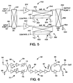
- FIG. 5 shows a schematic block diagram of a phase shifter and low-noise switch 10d of another SPDT switch according to another embodiment of the present invention that significantly parallels the structure of the switch 10 above.
- the output port 50d includes a load resistor 54d.
- State Table 5 below gives the output states at the output port 48d with respect to the input signals S1 and S2 at the input ports 14d and 16d, respectively. Particularly, if the gate terminal ports 32d and 44d are both biased, then the output signal at the output port 48d is the gain G times the input signal S2 at the phase angle ⁇ .
- the output signal at the output port 48d is the gain G times the input signal S2 at the phase angle ⁇ + 180°. If the port 32d is biased and the port 44d is unbiased, then the signal at the output port 48d is the gain G times the input signal S1 at the phase angle ⁇ . If the port 32d is unbiased and the port 44d is biased, then the output signal at the port 44d is the gain G times the input signal S1 at the phase angle ⁇ + 180°. In this embodiment, the input signals S1 and S2 can be selectively applied to the output port 48d depending on the bias of the control ports 32d and 44d.
- the switch 10a has application as a BSLNA at an input stage of a thermal imager well known to those skilled in the art.
- Thermal imagers generally act passively in that they sense radiation at particular wavelengths, such as infrared, without the imager emitting an excitation signal that is reflected off of objects in the scene.
- These types of systems incorporate antenna arrays having many antenna elements where each element is a pixel of the image. Each antenna element receives thermal radiation from the scene, which is selectively output to an imaging device typically on a pixel-by-pixel basis. Because this type of thermal imager acts passively, the radiation signal received by the antenna elements is fairly small relative to electronic noise in the system.
- the BSLNA 10a becomes useful in these types of devices where noise in the system is continuously applied to the output port 48a when the gate ports 32a and 44a are unbiased, and then noise of the system and the RF signal S1 at the input port 14a are applied to the output port 48a when the control gate port 32a is biased. In this manner, the subsequent processing circuitry can separate the noise of the system and provide a relatively more stable amplified RF signal S1.
- FIG 6 is a schematic block diagram of a balanced radiometer 62 (thermal imager) incorporating a BSLNA 64 of the same type as the switch 10a of Figure 3 above.
- the BSLNA 64 includes a hybrid coupler 66 that separates the BSLNA 64 into a first path 68 and a second path 70.
- the first path 68 includes two amplifiers 72 intended to represent the amplifier 22a
- the second path 70 includes two amplifiers 74 intended to represent the amplifier 34a.
- the first path 68 includes a phase shifter 76 intended to represent the phase shifter 24, and the second path 70 includes phase shifter 78 intended to represent the phase shifter 36a.
- a hybrid coupler 80 couples an output from the first path 68 and the second path 70 into a series of buffer amplifiers 82.
- the output of the BSLNA 64 can be selectively switched between an input signal from an antenna 84 or an impedance matched noise signal from an input load resistor 86.
- the amplified signal from the buffer amplifiers 82 is applied to an amplifier 88 including a coupler 90.
- the coupler 90 separates the signal into a first amplifier path including an amplifier 92 and a second amplifier path including an amplifier 94.
- the outputs from the amplifiers 92 and 94 are applied to another coupler 96 that couples the signal into a diode detector 98.
- the diode detector 98 converts the RF signals to comparable DC level signals for subsequent signal processing.
Landscapes
- Amplifiers (AREA)
- Electronic Switches (AREA)
- Variable-Direction Aerials And Aerial Arrays (AREA)
- Waveguide Switches, Polarizers, And Phase Shifters (AREA)
Applications Claiming Priority (2)
| Application Number | Priority Date | Filing Date | Title |
|---|---|---|---|
| US08/440,555 US5606283A (en) | 1995-05-12 | 1995-05-12 | Monolithic multi-function balanced switch and phase shifter |
| US440555 | 1995-05-12 |
Publications (2)
| Publication Number | Publication Date |
|---|---|
| EP0742602A2 true EP0742602A2 (de) | 1996-11-13 |
| EP0742602A3 EP0742602A3 (de) | 1998-03-11 |
Family
ID=23749226
Family Applications (1)
| Application Number | Title | Priority Date | Filing Date |
|---|---|---|---|
| EP96106374A Withdrawn EP0742602A3 (de) | 1995-05-12 | 1996-04-23 | Monolithischer multifunktioneller balancierter Schalter und Phasenschieber |
Country Status (4)
| Country | Link |
|---|---|
| US (1) | US5606283A (de) |
| EP (1) | EP0742602A3 (de) |
| JP (1) | JPH08335801A (de) |
| KR (1) | KR100189309B1 (de) |
Cited By (3)
| Publication number | Priority date | Publication date | Assignee | Title |
|---|---|---|---|---|
| EP0825452A2 (de) * | 1996-08-13 | 1998-02-25 | Trw Inc. | Monolithischer, rauscharmer, synchroner Empfänger mit "Direkt-Detektion" für passive radiometrische Abbildungssysteme im Mikro/Millimeter Wellenbereich |
| KR100515028B1 (ko) * | 2002-07-30 | 2005-09-15 | 국방과학연구소 | 멀티-폴드 랑게 커플러를 사용한 mmic 위상변위기 |
| WO2020016483A1 (en) * | 2018-07-18 | 2020-01-23 | Teknologian Tutkimuskeskus Vtt Oy | Active noise source design |
Families Citing this family (27)
| Publication number | Priority date | Publication date | Assignee | Title |
|---|---|---|---|---|
| US5778306A (en) * | 1996-11-08 | 1998-07-07 | Motorola Inc. | Low loss high frequency transmitting/receiving switching module |
| US6020848A (en) * | 1998-01-27 | 2000-02-01 | The Boeing Company | Monolithic microwave integrated circuits for use in low-cost dual polarization phased-array antennas |
| US6690238B2 (en) * | 2000-12-27 | 2004-02-10 | Emhiser Research, Inc. | Variable phase-shifting rf power amplifiers |
| US6747517B2 (en) | 2000-12-27 | 2004-06-08 | Emhiser Research, Inc. | Power-shifting rf amplifiers |
| GB0102384D0 (en) * | 2001-01-31 | 2001-03-14 | Secr Defence | Signal detection using a phased array antenna |
| EP1428289A1 (de) * | 2001-09-20 | 2004-06-16 | Paratek Microwave, Inc. | Abstimmbare filter mit variabler bandbreite und variabler verzögerung |
| US7034636B2 (en) * | 2001-09-20 | 2006-04-25 | Paratek Microwave Incorporated | Tunable filters having variable bandwidth and variable delay |
| US6636116B2 (en) * | 2001-10-05 | 2003-10-21 | Texas Instruments Incorporated | Fully differential current feedback amplifier |
| KR100536189B1 (ko) * | 2002-07-30 | 2005-12-14 | 국방과학연구소 | 광대역 180°-비트 위상변위기 |
| DE10308848A1 (de) * | 2003-02-27 | 2004-09-09 | Marconi Communications Gmbh | Integrierte Verstärkeranordnung |
| US7088086B2 (en) | 2003-09-18 | 2006-08-08 | Xytrans, Inc. | Multi-channel radiometer imaging system |
| US7254374B2 (en) * | 2004-07-21 | 2007-08-07 | Spx Corporation | Switchable multi-transmitter combiner and method |
| US7831222B1 (en) * | 2006-02-24 | 2010-11-09 | Clear Channel Management Services, Inc. | Method and apparatus for improving the isolation characteristics of HD radio combiners |
| US20080143456A1 (en) * | 2006-12-15 | 2008-06-19 | Isotek Electronics Limited | Band combining filter |
| US20080219246A1 (en) * | 2007-03-08 | 2008-09-11 | Northrop Grumman Space And Mission Systems Corp. | System and method for switching using coordinated phase shifters |
| US7791536B2 (en) * | 2007-06-24 | 2010-09-07 | Raytheon Company | High power phased array antenna system and method with low power switching |
| US8213672B2 (en) | 2007-08-08 | 2012-07-03 | Microsemi Corporation | Millimeter wave imaging method and system to detect concealed objects |
| JP4893654B2 (ja) * | 2008-02-19 | 2012-03-07 | 日本電気株式会社 | 電力合成方法、電力分配方法、電力合成分配器及び無線通信装置 |
| US8295212B2 (en) * | 2009-08-05 | 2012-10-23 | Alcatel Lucent | System and method for TDD/TMA with hybrid bypass switch of receiving amplifier |
| US8866079B2 (en) * | 2010-02-04 | 2014-10-21 | International Business Machines Corporation | Compact imaging receiver architecture |
| US8314654B2 (en) * | 2010-05-17 | 2012-11-20 | Alcatel Lucent | Multi-band high-efficiency Doherty amplifier |
| JP2013110638A (ja) * | 2011-11-22 | 2013-06-06 | Mitsubishi Electric Corp | マルチポートフィードフォワード増幅器 |
| US9143366B2 (en) * | 2012-09-07 | 2015-09-22 | The Aerospace Corporation | Galvanic isolation interface for high-speed data link for spacecraft electronics, and method of using same |
| TWI518993B (zh) | 2012-11-20 | 2016-01-21 | 財團法人工業技術研究院 | 具可調式相移陣列的多路徑切換系統 |
| JP5768087B2 (ja) * | 2013-05-16 | 2015-08-26 | 株式会社東芝 | 半導体電力増幅器 |
| US20150035619A1 (en) * | 2013-08-02 | 2015-02-05 | Electronics And Telecommunications Research Institute | Phase shifter and method of shifting phase of signal |
| KR102654491B1 (ko) * | 2016-06-16 | 2024-04-04 | 주식회사 유텔 | 마이크로파 멀티칩 패키지 장치 |
Family Cites Families (40)
| Publication number | Priority date | Publication date | Assignee | Title |
|---|---|---|---|---|
| US3346823A (en) * | 1964-12-18 | 1967-10-10 | John W Maurer | Passive device for obtaining independent amplitude and phase control of a uhf or microwave signal |
| US3571765A (en) * | 1969-09-15 | 1971-03-23 | Bell Telephone Labor Inc | Quantized phase shifter utilizing open-circuited or short-circuited 3db quadrature couplers |
| US3769610A (en) * | 1972-06-15 | 1973-10-30 | Philco Ford Corp | Voltage controlled variable power divider |
| US4016516A (en) * | 1974-05-28 | 1977-04-05 | American Nucleonics Corporation | Reflective signal controller |
| US3931599A (en) * | 1975-01-30 | 1976-01-06 | Edward Salzberg | Hybrid phase inverter |
| US4016503A (en) * | 1975-07-24 | 1977-04-05 | Westinghouse Electric Corporation | High-reliability power amplifier |
| GB1559974A (en) * | 1976-09-16 | 1980-01-30 | Marconi Co Ltd | Electrical transmission system |
| US4153886A (en) * | 1978-02-17 | 1979-05-08 | Bell Telephone Laboratories, Incorporated | Ninety degree phase stepper |
| US4254385A (en) * | 1978-08-31 | 1981-03-03 | Communications Satellite Corporation | Two-dimensional (planar) TDMA/broadcast microwave switch matrix for switched satellite application |
| US4352071A (en) * | 1979-06-22 | 1982-09-28 | Communications Satellite Corporation | Planar QPSK demodulator |
| DE3122084A1 (de) * | 1981-06-03 | 1983-01-05 | Siemens AG, 1000 Berlin und 8000 München | Frequenzweiche zur trennung eines signal- und eines versorgungsstromes |
| US4549152A (en) * | 1983-03-28 | 1985-10-22 | Rca Corporation | Broadband adjustable phase modulation circuit |
| US4602227A (en) * | 1984-07-30 | 1986-07-22 | Rca Corporation | Coaxial LC phase-shifter for phase-controlled television broadcast switching circuit |
| US4631493A (en) * | 1985-03-18 | 1986-12-23 | Eaton Corporation | Circuit for DC biasing |
| US4723307A (en) * | 1986-01-31 | 1988-02-02 | General Signal Corporation | Simplified phase-controlled television broadcast switching circuit and three-position coaxial LC phase shifter therefor |
| US5081706A (en) * | 1987-07-30 | 1992-01-14 | Texas Instruments Incorporated | Broadband merged switch |
| US4825177A (en) * | 1987-10-16 | 1989-04-25 | General Instrument Corporation | Microwave amplifier and other microwave components |
| US4978932A (en) * | 1988-07-07 | 1990-12-18 | Communications Satellite Corporation | Microwave digitally controlled solid-state attenuator having parallel switched paths |
| US4939485A (en) * | 1988-12-09 | 1990-07-03 | Varian Associates, Inc. | Microwave field effect switch |
| JP2665251B2 (ja) * | 1989-02-15 | 1997-10-22 | 富士通株式会社 | マイクロ波増幅器 |
| US5023494A (en) * | 1989-10-20 | 1991-06-11 | Raytheon Company | High isolation passive switch |
| US5027084A (en) * | 1989-11-30 | 1991-06-25 | Raytheon Company | Transceiver modules for phased array antenna |
| US5006811A (en) * | 1990-01-31 | 1991-04-09 | Triquint Semiconductor, Inc. | Dual quadrature frequency converter |
| US5061911A (en) * | 1990-04-03 | 1991-10-29 | Motorola, Inc. | Single fault/tolerant MMIC switches |
| US5119050A (en) * | 1990-04-26 | 1992-06-02 | Upshur John I | Low loss 360 degree x-band analog phase shifter |
| JPH0421201A (ja) * | 1990-05-16 | 1992-01-24 | Toyota Central Res & Dev Lab Inc | 移相器 |
| US5086329A (en) * | 1990-07-27 | 1992-02-04 | The United States Of America As Represented By The Secretary Of The Navy | Planar gallium arsenide NPNP microwave switch |
| US5053719A (en) * | 1990-08-13 | 1991-10-01 | Raytheon Company | Wide-band push-pull amplifier |
| US5122690A (en) * | 1990-10-16 | 1992-06-16 | General Electric Company | Interface circuits including driver circuits with switching noise reduction |
| US5222246A (en) * | 1990-11-02 | 1993-06-22 | General Electric Company | Parallel amplifiers with combining phase controlled from combiner difference port |
| US5101171A (en) * | 1990-11-23 | 1992-03-31 | Advanced Systems Research, Inc. | Extended bandwidth RF amplifier |
| US5105171A (en) * | 1991-04-29 | 1992-04-14 | Hughes Aircraft Company | Coplanar waveguide directional coupler and flip-clip microwave monolithic integrated circuit assembly incorporating the coupler |
| US5146177A (en) * | 1991-08-30 | 1992-09-08 | General Electric Co. | Balanced reflective nonlinear processor using FETs |
| US5289142A (en) * | 1992-03-31 | 1994-02-22 | Raytheon Company | Transmit/receive switch for phased array antenna |
| JP2758531B2 (ja) * | 1992-04-22 | 1998-05-28 | 三菱電機株式会社 | 半導体装置 |
| US5302958A (en) * | 1992-07-08 | 1994-04-12 | Ems Technologies, Inc. | Low loss, fast switching, tunable filter circuit |
| US5254492A (en) * | 1992-11-10 | 1993-10-19 | Texas Instruments Incorporated | Method of fabricating an integrated circuit for providing low-noise and high-power microwave operation |
| JPH06338702A (ja) * | 1993-05-31 | 1994-12-06 | Mitsubishi Electric Corp | 反射型移相器及び多ビット移相器 |
| US5375257A (en) * | 1993-12-06 | 1994-12-20 | Raytheon Company | Microwave switch |
| US5392009A (en) * | 1993-12-22 | 1995-02-21 | American Nucleonics Corporation | Low current vector modulator |
-
1995
- 1995-05-12 US US08/440,555 patent/US5606283A/en not_active Expired - Lifetime
-
1996
- 1996-04-23 EP EP96106374A patent/EP0742602A3/de not_active Withdrawn
- 1996-05-11 KR KR1019960016070A patent/KR100189309B1/ko not_active Expired - Fee Related
- 1996-05-13 JP JP8117354A patent/JPH08335801A/ja active Pending
Cited By (4)
| Publication number | Priority date | Publication date | Assignee | Title |
|---|---|---|---|---|
| EP0825452A2 (de) * | 1996-08-13 | 1998-02-25 | Trw Inc. | Monolithischer, rauscharmer, synchroner Empfänger mit "Direkt-Detektion" für passive radiometrische Abbildungssysteme im Mikro/Millimeter Wellenbereich |
| KR100515028B1 (ko) * | 2002-07-30 | 2005-09-15 | 국방과학연구소 | 멀티-폴드 랑게 커플러를 사용한 mmic 위상변위기 |
| WO2020016483A1 (en) * | 2018-07-18 | 2020-01-23 | Teknologian Tutkimuskeskus Vtt Oy | Active noise source design |
| US11953535B2 (en) | 2018-07-18 | 2024-04-09 | Teknologian Tutkimuskeskus Vtt Oy | Active noise source design |
Also Published As
| Publication number | Publication date |
|---|---|
| US5606283A (en) | 1997-02-25 |
| JPH08335801A (ja) | 1996-12-17 |
| KR960043346A (ko) | 1996-12-23 |
| EP0742602A3 (de) | 1998-03-11 |
| KR100189309B1 (ko) | 1999-06-01 |
Similar Documents
| Publication | Publication Date | Title |
|---|---|---|
| US5606283A (en) | Monolithic multi-function balanced switch and phase shifter | |
| US4959873A (en) | Transmission line switch | |
| US4637073A (en) | Transmit/receive switch | |
| US5446464A (en) | Transceiver module | |
| US5375257A (en) | Microwave switch | |
| US7239852B2 (en) | Asymmetric, optimized common-source bi-directional amplifier | |
| US6281762B1 (en) | SPST switch, SPDT switch, and communication apparatus using the SPDT switch | |
| US7936237B2 (en) | Multi-band transmit-receive switch for wireless transceiver | |
| US6020848A (en) | Monolithic microwave integrated circuits for use in low-cost dual polarization phased-array antennas | |
| EP0729670B1 (de) | Bidirektionaler verstaerker | |
| US4983865A (en) | High speed switch matrix | |
| US7079815B2 (en) | Monolithic microwave integrated circuit transceiver | |
| US20030220081A1 (en) | Transceiver circuit arrangement and method | |
| US6265953B1 (en) | Apparatus and method for enhancing the isolation of an MMIC cross-point switch | |
| US6657497B1 (en) | Asymmetric, voltage optimized, wideband common-gate bi-directional MMIC amplifier | |
| US12199578B2 (en) | Amplifiers suitable for mm-wave signal splitting and combining | |
| US5323064A (en) | Radio frequency signal frequency converter | |
| US8190099B2 (en) | Switch-less bidirectional amplifier | |
| Min et al. | SiGe T/R modules for Ka-band phased arrays | |
| EP1374395B1 (de) | Wanderwellenverstärker | |
| Zuefle et al. | Coplanar 4-bit HEMT phase shifters for 94 GHz phased array radar systems | |
| Shiba et al. | F-band bidirectional amplifier using 75-nm InP HEMTs | |
| HK123497A (en) | Combining technique for a multistage, parallel amplifier | |
| WO2001052426A2 (en) | Improved mmic transceiver | |
| Hyashi et al. | IF-band MMICs for high-speed wireless signal processing |
Legal Events
| Date | Code | Title | Description |
|---|---|---|---|
| PUAI | Public reference made under article 153(3) epc to a published international application that has entered the european phase |
Free format text: ORIGINAL CODE: 0009012 |
|
| AK | Designated contracting states |
Kind code of ref document: A2 Designated state(s): DE FR GB |
|
| PUAL | Search report despatched |
Free format text: ORIGINAL CODE: 0009013 |
|
| AK | Designated contracting states |
Kind code of ref document: A3 Designated state(s): DE FR GB |
|
| STAA | Information on the status of an ep patent application or granted ep patent |
Free format text: STATUS: THE APPLICATION HAS BEEN WITHDRAWN |
|
| 17P | Request for examination filed |
Effective date: 19980407 |
|
| 18W | Application withdrawn |
Withdrawal date: 19980423 |