EP0742623B1 - Dispositif optique à semi-conducteur, sa méthode de commande, l'utilisation du dispositif comme source de lumière et système de communication comportant une telle source - Google Patents
Dispositif optique à semi-conducteur, sa méthode de commande, l'utilisation du dispositif comme source de lumière et système de communication comportant une telle source Download PDFInfo
- Publication number
- EP0742623B1 EP0742623B1 EP96106666A EP96106666A EP0742623B1 EP 0742623 B1 EP0742623 B1 EP 0742623B1 EP 96106666 A EP96106666 A EP 96106666A EP 96106666 A EP96106666 A EP 96106666A EP 0742623 B1 EP0742623 B1 EP 0742623B1
- Authority
- EP
- European Patent Office
- Prior art keywords
- region
- semiconductor device
- lossy
- optical semiconductor
- gain
- Prior art date
- Legal status (The legal status is an assumption and is not a legal conclusion. Google has not performed a legal analysis and makes no representation as to the accuracy of the status listed.)
- Expired - Lifetime
Links
Images









Classifications
-
- B—PERFORMING OPERATIONS; TRANSPORTING
- B82—NANOTECHNOLOGY
- B82Y—SPECIFIC USES OR APPLICATIONS OF NANOSTRUCTURES; MEASUREMENT OR ANALYSIS OF NANOSTRUCTURES; MANUFACTURE OR TREATMENT OF NANOSTRUCTURES
- B82Y20/00—Nanooptics, e.g. quantum optics or photonic crystals
-
- H—ELECTRICITY
- H01—ELECTRIC ELEMENTS
- H01S—DEVICES USING THE PROCESS OF LIGHT AMPLIFICATION BY STIMULATED EMISSION OF RADIATION [LASER] TO AMPLIFY OR GENERATE LIGHT; DEVICES USING STIMULATED EMISSION OF ELECTROMAGNETIC RADIATION IN WAVE RANGES OTHER THAN OPTICAL
- H01S5/00—Semiconductor lasers
- H01S5/02—Structural details or components not essential to laser action
- H01S5/026—Monolithically integrated components, e.g. waveguides, monitoring photo-detectors, drivers
- H01S5/0265—Intensity modulators
-
- H—ELECTRICITY
- H01—ELECTRIC ELEMENTS
- H01S—DEVICES USING THE PROCESS OF LIGHT AMPLIFICATION BY STIMULATED EMISSION OF RADIATION [LASER] TO AMPLIFY OR GENERATE LIGHT; DEVICES USING STIMULATED EMISSION OF ELECTROMAGNETIC RADIATION IN WAVE RANGES OTHER THAN OPTICAL
- H01S5/00—Semiconductor lasers
- H01S5/06—Arrangements for controlling the laser output parameters, e.g. by operating on the active medium
- H01S5/062—Arrangements for controlling the laser output parameters, e.g. by operating on the active medium by varying the potential of the electrodes
- H01S5/0625—Arrangements for controlling the laser output parameters, e.g. by operating on the active medium by varying the potential of the electrodes in multi-section lasers
-
- H—ELECTRICITY
- H01—ELECTRIC ELEMENTS
- H01S—DEVICES USING THE PROCESS OF LIGHT AMPLIFICATION BY STIMULATED EMISSION OF RADIATION [LASER] TO AMPLIFY OR GENERATE LIGHT; DEVICES USING STIMULATED EMISSION OF ELECTROMAGNETIC RADIATION IN WAVE RANGES OTHER THAN OPTICAL
- H01S5/00—Semiconductor lasers
- H01S5/10—Construction or shape of the optical resonator, e.g. extended or external cavity, coupled cavities, bent-guide, varying width, thickness or composition of the active region
- H01S5/12—Construction or shape of the optical resonator, e.g. extended or external cavity, coupled cavities, bent-guide, varying width, thickness or composition of the active region the resonator having a periodic structure, e.g. in distributed feedback [DFB] lasers
-
- H—ELECTRICITY
- H01—ELECTRIC ELEMENTS
- H01S—DEVICES USING THE PROCESS OF LIGHT AMPLIFICATION BY STIMULATED EMISSION OF RADIATION [LASER] TO AMPLIFY OR GENERATE LIGHT; DEVICES USING STIMULATED EMISSION OF ELECTROMAGNETIC RADIATION IN WAVE RANGES OTHER THAN OPTICAL
- H01S5/00—Semiconductor lasers
- H01S5/50—Amplifier structures not provided for in groups H01S5/02 - H01S5/30
- H01S5/5036—Amplifier structures not provided for in groups H01S5/02 - H01S5/30 the arrangement being polarisation-selective
-
- H—ELECTRICITY
- H04—ELECTRIC COMMUNICATION TECHNIQUE
- H04B—TRANSMISSION
- H04B10/00—Transmission systems employing electromagnetic waves other than radio-waves, e.g. infrared, visible or ultraviolet light, or employing corpuscular radiation, e.g. quantum communication
- H04B10/50—Transmitters
- H04B10/516—Details of coding or modulation
- H04B10/532—Polarisation modulation
-
- H—ELECTRICITY
- H01—ELECTRIC ELEMENTS
- H01S—DEVICES USING THE PROCESS OF LIGHT AMPLIFICATION BY STIMULATED EMISSION OF RADIATION [LASER] TO AMPLIFY OR GENERATE LIGHT; DEVICES USING STIMULATED EMISSION OF ELECTROMAGNETIC RADIATION IN WAVE RANGES OTHER THAN OPTICAL
- H01S2301/00—Functional characteristics
- H01S2301/14—Semiconductor lasers with special structural design for lasing in a specific polarisation mode
-
- H—ELECTRICITY
- H01—ELECTRIC ELEMENTS
- H01S—DEVICES USING THE PROCESS OF LIGHT AMPLIFICATION BY STIMULATED EMISSION OF RADIATION [LASER] TO AMPLIFY OR GENERATE LIGHT; DEVICES USING STIMULATED EMISSION OF ELECTROMAGNETIC RADIATION IN WAVE RANGES OTHER THAN OPTICAL
- H01S5/00—Semiconductor lasers
- H01S5/06—Arrangements for controlling the laser output parameters, e.g. by operating on the active medium
-
- H—ELECTRICITY
- H01—ELECTRIC ELEMENTS
- H01S—DEVICES USING THE PROCESS OF LIGHT AMPLIFICATION BY STIMULATED EMISSION OF RADIATION [LASER] TO AMPLIFY OR GENERATE LIGHT; DEVICES USING STIMULATED EMISSION OF ELECTROMAGNETIC RADIATION IN WAVE RANGES OTHER THAN OPTICAL
- H01S5/00—Semiconductor lasers
- H01S5/06—Arrangements for controlling the laser output parameters, e.g. by operating on the active medium
- H01S5/0601—Arrangements for controlling the laser output parameters, e.g. by operating on the active medium comprising an absorbing region
-
- H—ELECTRICITY
- H01—ELECTRIC ELEMENTS
- H01S—DEVICES USING THE PROCESS OF LIGHT AMPLIFICATION BY STIMULATED EMISSION OF RADIATION [LASER] TO AMPLIFY OR GENERATE LIGHT; DEVICES USING STIMULATED EMISSION OF ELECTROMAGNETIC RADIATION IN WAVE RANGES OTHER THAN OPTICAL
- H01S5/00—Semiconductor lasers
- H01S5/06—Arrangements for controlling the laser output parameters, e.g. by operating on the active medium
- H01S5/062—Arrangements for controlling the laser output parameters, e.g. by operating on the active medium by varying the potential of the electrodes
- H01S5/06233—Controlling other output parameters than intensity or frequency
- H01S5/06236—Controlling other output parameters than intensity or frequency controlling the polarisation, e.g. TM/TE polarisation switching
-
- H—ELECTRICITY
- H01—ELECTRIC ELEMENTS
- H01S—DEVICES USING THE PROCESS OF LIGHT AMPLIFICATION BY STIMULATED EMISSION OF RADIATION [LASER] TO AMPLIFY OR GENERATE LIGHT; DEVICES USING STIMULATED EMISSION OF ELECTROMAGNETIC RADIATION IN WAVE RANGES OTHER THAN OPTICAL
- H01S5/00—Semiconductor lasers
- H01S5/06—Arrangements for controlling the laser output parameters, e.g. by operating on the active medium
- H01S5/062—Arrangements for controlling the laser output parameters, e.g. by operating on the active medium by varying the potential of the electrodes
- H01S5/0625—Arrangements for controlling the laser output parameters, e.g. by operating on the active medium by varying the potential of the electrodes in multi-section lasers
- H01S5/06255—Controlling the frequency of the radiation
- H01S5/06258—Controlling the frequency of the radiation with DFB-structure
-
- H—ELECTRICITY
- H01—ELECTRIC ELEMENTS
- H01S—DEVICES USING THE PROCESS OF LIGHT AMPLIFICATION BY STIMULATED EMISSION OF RADIATION [LASER] TO AMPLIFY OR GENERATE LIGHT; DEVICES USING STIMULATED EMISSION OF ELECTROMAGNETIC RADIATION IN WAVE RANGES OTHER THAN OPTICAL
- H01S5/00—Semiconductor lasers
- H01S5/30—Structure or shape of the active region; Materials used for the active region
- H01S5/34—Structure or shape of the active region; Materials used for the active region comprising quantum well or superlattice structures, e.g. single quantum well [SQW] lasers, multiple quantum well [MQW] lasers or graded index separate confinement heterostructure [GRINSCH] lasers
- H01S5/3403—Structure or shape of the active region; Materials used for the active region comprising quantum well or superlattice structures, e.g. single quantum well [SQW] lasers, multiple quantum well [MQW] lasers or graded index separate confinement heterostructure [GRINSCH] lasers having a strained layer structure in which the strain performs a special function, e.g. general strain effects, strain versus polarisation
- H01S5/3404—Structure or shape of the active region; Materials used for the active region comprising quantum well or superlattice structures, e.g. single quantum well [SQW] lasers, multiple quantum well [MQW] lasers or graded index separate confinement heterostructure [GRINSCH] lasers having a strained layer structure in which the strain performs a special function, e.g. general strain effects, strain versus polarisation influencing the polarisation
-
- H—ELECTRICITY
- H01—ELECTRIC ELEMENTS
- H01S—DEVICES USING THE PROCESS OF LIGHT AMPLIFICATION BY STIMULATED EMISSION OF RADIATION [LASER] TO AMPLIFY OR GENERATE LIGHT; DEVICES USING STIMULATED EMISSION OF ELECTROMAGNETIC RADIATION IN WAVE RANGES OTHER THAN OPTICAL
- H01S5/00—Semiconductor lasers
- H01S5/30—Structure or shape of the active region; Materials used for the active region
- H01S5/34—Structure or shape of the active region; Materials used for the active region comprising quantum well or superlattice structures, e.g. single quantum well [SQW] lasers, multiple quantum well [MQW] lasers or graded index separate confinement heterostructure [GRINSCH] lasers
- H01S5/3408—Structure or shape of the active region; Materials used for the active region comprising quantum well or superlattice structures, e.g. single quantum well [SQW] lasers, multiple quantum well [MQW] lasers or graded index separate confinement heterostructure [GRINSCH] lasers characterised by specially shaped wells, e.g. triangular
-
- H—ELECTRICITY
- H01—ELECTRIC ELEMENTS
- H01S—DEVICES USING THE PROCESS OF LIGHT AMPLIFICATION BY STIMULATED EMISSION OF RADIATION [LASER] TO AMPLIFY OR GENERATE LIGHT; DEVICES USING STIMULATED EMISSION OF ELECTROMAGNETIC RADIATION IN WAVE RANGES OTHER THAN OPTICAL
- H01S5/00—Semiconductor lasers
- H01S5/40—Arrangement of two or more semiconductor lasers, not provided for in groups H01S5/02 - H01S5/30
- H01S5/4025—Array arrangements, e.g. constituted by discrete laser diodes or laser bar
- H01S5/4031—Edge-emitting structures
- H01S5/4043—Edge-emitting structures with vertically stacked active layers
Definitions
- the present invention relates to optical semiconductor devices, such as an optical filter, a tunable semiconductor laser, and an oscillation polarization selective semiconductor laser whose mode state of polarization of oscillated light can be switched, which are suitable for a light source and the like used in optical communications, optical information processing, such as an optical memory, optical operations and optical computers, and so forth.
- the present invention further relates to a driving method for driving the optical semiconductor device and an optical communication system using the optical semiconductor device as a light source in a transmitter or the like.
- a semiconductor laser is continuously driven (CW driving) and the continuous light wave from the laser is intensity-modulated by an external modulator which uses a dielectric material, a semiconductor or the like.
- This method has drawbacks in that there are limitations to down-sizing and cost reduction of the device and in that flexibility of optical networks (capability of simultaneous transmission of signals whose speeds are greatly different, etc.) is not high.
- the oscillation polarization is changed from TM mode to TE mode at a given current point, and the threshold gain is selectively reached between TE mode and TM mode by a signal current with a constant current for simultaneous oscillation of TE and TM modes being injected as a bias point.
- the polarization-modulated light from the semiconductor laser is transmitted through a polarizer and only light polarized in a given direction is transmitted over a transmission line.
- carrier fluctuation accompanying the modulation can be notably decreased in the device since light density in the semiconductor laser remains unchanged during the modulation (i.e., a driving current is always almost constant and not "ON-OFFed").
- a driving current is always almost constant and not "ON-OFFed"
- optical semiconductor devices such as an oscillation polarization selective semiconductor laser in which chirping is greatly reduced and which can be readily fabricated, a tunable semiconductor laser with a reduced chirping and a tunable semiconductor filter whose transmission property is insensitive to polarization, a driving method for driving the optical semiconductor device, and an optical communication system and the like using the optical semiconductor device.
- gain spectrum and cavity loss spectrum can be independently controlled, so that characteristics of the device are improved and a degree of freedom in design is increased. Thus, fabrication yield is improved.
- relations (1)-(3) can be readily satisfied by controlling polarization dependencies of both of the gain region and the lossy region.
- an effective refractive index of the light waveguide can be changed by the tuning or wavelength control region, such as a tuning layer, formed independently from the gain control means and the loss control means, and the wavelength determined by relation (2) can be controlled by the tuning means independently from the the gain control means and the loss control means. This is in sharp contrast to a prior art device in which the gain control and the wavelength control are not independent from each other.
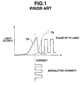
- Fig. 1 is a graph for explaining a prior art semiconductor laser whose oscillation polarization mode can be switched between TE and TM modes.
- Fig. 2 is a longitudinal cross-sectional view taken along a cavity direction showing the structure of a first embodiment of an oscillation polarization selective semiconductor laser according to the present invention.
- Fig. 3 is a diagram of the energy band structure of an active layer and layers adjacent thereto or a lossy layer and layers adjacent thereto formed in the first embodiment and other embodiments.
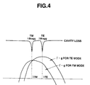
- Fig. 4 is a graph illustrating the relationship between gains (more accurately ⁇ g) for TE and TM modes and cavity losses ( ⁇ ⁇ ⁇ in + ⁇ M + ⁇ SC ) at the time when carriers are uniformly injected into a gain region or gain regions of the first embodiment and other embodiments.
- Fig. 5 is a graph illustrating the relationship between gains (more accurately ⁇ g) for TE and TM modes and cavity losses ( ⁇ ⁇ ⁇ in + ⁇ M + ⁇ SC ) at the time when carriers are unevenly injected into a gain region or gain regions of the first embodiment and other embodiments to change the correlation of gains for TE and TM modes and a reverse voltage is applied to a lossy region.
- Fig. 6 is a g-raph schematically illustrating the relationships between operation current and line width in the first embodiment and a prior art.
- Fig. 7 is a graph schematically illustrating a difference between the first embodiment and a prior art in a range in which. the oscillation polarization mode switching is possible, by using the relationship between operation current and light output.
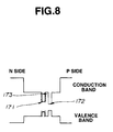
- Fig. 8 is a diagram of the energy band structure of an active layer and layers adjacent thereto formed in a second embodiment and other embodiments of the present invention.
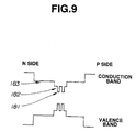
- Fig. 9 is a diagram of the energy band structure of a lossy layer and layers adjacent thereto formed in the second embodiment and other embodiments of the present invention.
- Fig. 10 is a graph illustrating the relationship between gains (more accurately ⁇ ⁇ g) for TE and TM modes and cavity losses ( ⁇ ⁇ ⁇ in + ⁇ M + ⁇ SC ) at the time when carriers are injected into a gain region or gain regions of the second embodiment and other embodiments and a voltage is applied to a lossy region of the second embodiment and other embodiments.
- Fig. 11 is a longitudinal cross-sectional view taken along a cavity direction showing the structure of a third embodiment of an oscillation polarization selective semiconductor laser according to the present invention.
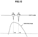
- Fig. 12 is a graph illustrating the relationship between gains (more accurately ⁇ ⁇ g) for TE and TM modes and cavity losses ( ⁇ ⁇ ⁇ in + ⁇ M + ⁇ SC ) at the time when carriers are independently injected into first and second gain regions of the third embodiment and a reverse voltage is applied to a lossy region of the third embodiment.
- Fig. 13 is a longitudinal cross-sectional view taken along a cavity direction showing the structure of a fourth embodiment of an optical semiconductor device according to the present invention.
- Fig. 14 is a transverse or lateral cross-sectional view taken along a lateral direction showing the structure of the fourth embodiment.
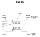
- Fig. 15 is a diagram of the energy band structure of a tuning layer and layers adjacent thereto formed in a sixth embodiment of the present invention.
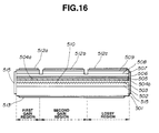
- Fig. 16 is a longitudinal cross-sectional view taken along a cavity direction showing the structure of a seventh embodiment of an optical semiconductor device according to the present invention.
- Fig. 17 is a transverse or lateral cross-sectional view taken along a lateral direction showing the structure of the seventh embodiment.
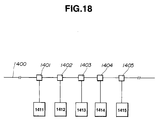
- Fig. 18 is a block diagram of a bus-type optical communication network according to the present invention.
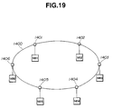
- Fig. 19 is a block diagram of a loop or ring-type optical communication network according to the present invention.
- the first embodiment is directed to an oscillation polarization selective semiconductor laser having a first gain region, a second gain region and a lossy region which are respectively arranged along a cavity or light propagation direction.
- the respective regions are electrically independent from each other, but optically coupled to each other through a common optical waveguide layer 103.
- the semiconductor laser of this embodiment includes an n-type InP substrate 101, an n-type InP cladding layer 102, the n-type InGaAsP lower optical waveguide layer 103, an undoped InGaAsP active layer 104a, an undoped InGaAsP lossy layer 104b, a p-type InP cladding layer 105, a p-type InGaAsP contact layer 106, positive or p-side electrodes 108a, 108b and 108c, and a negative or n-side electrode 109.
- a grating 107 is formed at a boundary between the n-type cladding layer 102 and the n-type optical waveguide layer 103.
- the grating 107 has a phase shift section (or some sections). Antireflection (AR) coatings 112 are provided on opposite end facets. The pitch of the grating 107 is set such that its Bragg wavelength for the TM mode is positioned at a gain peak wavelength.
- the active layer 104a in the first and second gain regions has the same structure as that of the lossy layer 104b in the lossy region.
- Each of the active layer 104a and the lossy layer 104b consists of five InGaAs well layers 121 (thickness: 10 nm and tensile strain: 1.0 %), InGaAsP barrier layers 122 (thickness: 10 nm and composition wavelength: 1.1 ⁇ m) and a pair of InGaAsP SCH (separate confinement heterostructure) layers 123 (thickness: 100 nm and composition wavelength: 1.2 ⁇ m).
- Energy band gap structures of the active layer 104a and the lossy layer 104b are illustrated in Fig. 3.
- Fig. 4 illustrates the relationship between gains (or more precisely, ⁇ ⁇ g) and cavity losses ( ⁇ ⁇ ⁇ in + ⁇ M + ⁇ SC ) for the TE mode and the TM mode at the time when carriers (about 10 18 cm -3 ) are uniformly injected into the first gain region and the second gain region.
- the abscissa indicates wavelength
- ⁇ TE / Bragg and ⁇ TM / Bragg respectively indicate Bragg wavelengths for the TE and TM modes
- ⁇ TE and ⁇ TM respectively indicate gain peak wavelengths for the TE and TM modes.
- Gain spectra or profiles for the TE and TM modes differ from each other because of the band structure of the strained quantum well active layer 104a.
- Fig. 5 illustrates the relationship between gains (or more precisely, ⁇ g) and cavity losses ( ⁇ ⁇ ⁇ in + ⁇ M + ⁇ SC ) for the TE mode and the TM mode at the time when carriers are unevenly injected into the first and second gain regions to change the gain correlation between the TE mode and the TM mode from that illustrated in Fig. 4 and a reverse voltage (e.g., about -5 V) is applied across the lossy region.
- a reverse voltage e.g., about -5 V
- oscillation polarization modulation can be performed by one of the following methods:
- Fig. 6 schematically illustrates relationships between operation current and line width of the first embodiment and a prior art device.
- a degree of difference between the first embodiment and the prior art device increases when the method (1) is used during the modulation.
- a range of operation current is wide while the line width varies within a narrow range at a low level in this embodiment.
- a range of operation current is narrow and the line width varies in a relatively wide range at a high level in the prior art device.
- Fig. 7 schematically illustrates relationships between operation current and light output intensity of the first embodiment and a prior art device to show a difference in polarization mode selective zones therebetween.
- a range of operation current is wide and the light output intensity can be varied over a wide range in this embodiment.
- a range of operation current is narrow and the light output intensity can be changed only in a narrow range in the prior art device.
- the polarization dependencies of both the gain region and the lossy region can be utilized and controlled, and hence, relations (1), (2) and (3) can be satisfied without any difficulty.
- an electric signal is superposed on a bias current or voltage in at least one of the gain regions and the lossy region and the oscillation polarization mode is switched as discussed above.
- the polarization dependency of wavelength dispersion can be speedily changed by QCSE.
- the total loss spectrum can have the polarization dependency and relations (1), (2) and (3) can be satisfied simultaneously.
- the loss can be speedily modulated by QCSE and one of the polarization modes can be selected. Further, gain or phase can be varied by changing the carrier density, and the polarization mode can be speedily switched between two polarization modes.
- the modulation efficiency is high when the light output intensity is the same, compared with a prior art device. Further, a range of light output intensity, in which oscillation polarization mode can be switched, is wide, as discussed above.
- FIG. 8 illustrates the band structure of an active layer of the second embodiment.
- Fig. 9 illustrates the band structure of a lossy layer of the second embodiment.
- the active layer of the second embodiment consists of an asymmetric strained dual quantum well structure including an InGaAs well layer 171, an InGaAsP well layer 172 and an InGaAsP barrier layer 173.
- a tensile strain of 1.0 % is introduced only into the InGaAs well layer 171 having a thickness of 10 nm, and no strain is introduced into either the InGaAsP well layer 172 (thickness: 10 nm, and energy gap wavelength: 1.65 ⁇ m) or the InGaAsP barrier layer 173 (thickness: 10 nm, and energy gap wavelength: 1.3 ⁇ m).
- the lossy layer of the second embodiment consists of two InGaAs well layers 181 (thickness: 10 nm, and tensile strain: 1.7 %), InGaAsP barrier layers 182 (thickness: 10 nm, and composition wavelength: 1.2 ⁇ m) and a pair of InGaAsP SCH layers 183 (thickness: 100 nm, and composition wavelength: 1.2 ⁇ m).
- the asymmetric quantum well structure has a larger freedom of variation in its bandgap than an ordinary quantum well structure, and further a strained asymmetric quantum well structure has a still larger freedom of variation in its bandgap than the asymmetric quantum well structure.
- bandgaps can be selectively or independently varied for different polarization modes (TE and TM modes). This means that gains generated in a common active layer by a common injection current density can be respectively set to threshold gains for different polarization modes (TE and TM modes).
- the threshold carrier density or injection current is set at a polarization modulation bias current point and a signal current is superimposed on the threshold injection current, for example, the oscillation polarization of output light can be switched between two polarization modes.
- the amplitude of the signal current superimposed on the bias current is small, so that the density of carriers in a laser cavity or resonator scarcely fluctuates. Therefore, the intensity of total output light scarcely varies during the polarization switching operation. Thus, chirping is substantially reduced.
- Fig. 10 illustrates the relationship between gains (accurately ⁇ ⁇ g) and cavity losses ( ⁇ ⁇ ⁇ in + ⁇ M + ⁇ SC ) for the TE mode and the TM mode at the time when carriers are injected into the first gain region and the second gain region and a voltage applied to the lossy region is controlled.
- the operation principle of I this embodiment is substantially the same as the first embodiment.
- the second embodiment differs from the first embodiment in that the structures of the gain regions and the lossy region are individually optimized as described above. As a result, the operation current can be further lowered, the modulation efficiency can be further enhanced, the line width can be further narrowed and the polarization mode selective zone can be further widened.
- FIG. 11 illustrates a cross-sectional view of the third embodiment taken along a cavity direction.
- a device of the third embodiment is divided into three portions along the cavity direction, i.e., a first gain region, a second gain region and a lossy region. Those regions are electrically independent from each other, but optically coupled to each other through a common optical waveguide layer 203, similar to the first embodiment.
- the semiconductor laser of this embodiment includes an n-type InP substrate 201, an n-type InP cladding layer 202, the n-type InGaAsP lower optical waveguide layer 203, an undoped InGaAsP active layer 204a, an undoped InGaAsP lossy layer 204b, a p-type InP cladding layer 205, a p-type InGaAsP contact layer 206, positive or p-side electrodes 208a, 208b and 208c, and a negative or n-side electrode 209.
- a grating 207 is formed at a boundary between the n-type cladding layer 202 and the n-type optical waveguide layer 203, and it has a phase shift section.
- Antireflection (AR) coatings 212 are provided on opposite end facets.
- the pitch of the grating 207 is set such that its Bragg wavelength for the TM mode is positioned at a gain peak wavelength.
- structures of the active layer 204a and the lossy layer 204b are the same (i.e., a bulk structure).
- the third embodiment is further different from the first embodiment in that the p-type cladding layer 205 in the lossy region is so thin that an electric field distribution of propagated light in the lossy region can extend to the electrode or loaded metal 208c. As a result, the lossy region only acts for propagated light wave in the TM mode.
- Fig. 12 illustrates the relationship between gains (more accurately ⁇ g) and cavity losses ( ⁇ in + ⁇ M + ⁇ SC ) for the TE mode and the TM mode at the time when carriers (about 10 18 cm -3 ) are uniformly injected into the first gain region and the second gain region to adjust the phase of DFB mode and a reverse bias voltage (about -5V) is applied to the lossy region.
- the abscissa indicates wavelength. Since the bulk active layer 204a is used, gain spectra for the TE mode and the TM mode are nearly the same. A peak value of the cavity loss spectrum for the TM mode is larger than that for the TE mode because of the loaded metal 208c which has a suppressing effect for the TM mode.
- relation (3) can be satisfied by adjusting the grating pitch such that gain at the Bragg wavelength for the TM mode is larger than that for the TE mode.
- the cavity loss profile can be controlled due to Franz-Keldysh (F-K) effect by applying a reverse voltage across the lossy region.
- the third embodiment features a polarization selective semiconductor laser that can be obtained by a simple fabrication method since the active layer and the lossy layer have the bulk structure.
- the operation principle of this embodiment is substantially the same as that of the first embodiment.
- loss can be imparted only to the TM mode by the loaded metal film on the waveguide surface of the lossy region.
- the oscillation polarization mode can be modulated, for example, by controlling the gain profile in the gain region.
- the F-K effect can speedily change the wavelength dispersion, and the total loss spectrum can have the polarization dependency by using a waveguide layer having the F-K effect in the lossy region.
- the oscillation polarization mode can also be modulated, for example, by controlling the loss profile in the lossy region.
- a fourth embodiment of the present invention will be described with reference to Figs. 3 through 5, 13 and 14.
- the fourth embodiment is directed to an optical semiconductor device having a gain region, a lossy region, a phase control region and a wavelength control region which are respectively arranged along a cavity or light propagation direction.
- the respective regions are electrically independent from each other, but optically coupled to each other through a common optical waveguide layer 303.
- the semiconductor device of this embodiment includes an n-type InP substrate 301, an n-type InP cladding layer 302, the n-type InGaAsP optical waveguide layer 303, an undoped InGaAsP active layer 304a, an undoped InGaAsP lossy layer 304b, an InGaAsP tuning layer 304c, a p-type InP upper cladding layer 305, a p-type InGaAsP contact or cap layer 306, positive or p-side electrodes 308a, 308b, 308c and 308d, and a negative or n-side electrode 309.
- a grating 307 is formed at a boundary between the n-type lower cladding layer 302 and the n-type optical waveguide layer 303 in the wavelength control region.
- the device of this embodiment is built as a distributed Bragg reflector type.
- reference numeral 311 is a ⁇ /2 coating provided on one end facet on the gain region side.
- a reference numeral 312 is an antireflection coating provided on the other end facet on the wavelength control region side.
- the pitch of the grating 307 is set such that its Bragg wavelength for the TM mode is positioned at a gain peak wavelength.
- the active layer 304a in the gain region has the same structure as the lossy layer 304b in the lossy region, similar to the first embodiment.
- reference numeral 310 designates a high-resistance InP burying layer.
- Each of the active layer 304a and the lossy layer 304b (or an absorptive layer) consists of five InGaAs well layers (thickness: 10 nm and tensile strain: 1.0 %), InGaAsP barrier layers (thickness: 10 nm and composition wavelength: 1.1 ⁇ m) and a pair of InGaAsP SCH layers (thickness: 100 nm and composition wavelength: 1.2 ⁇ m).
- Energy band gap structures of the active layer 304a and the lossy layer 304b are the same as that illustrated in Fig. 3.
- Fig. 4 also illustrates the relationship between gains (or more precisely, ⁇ g) and cavity losses ( ⁇ ⁇ ⁇ in + ⁇ M + ⁇ SC ) for the TE mode and the TM mode at the time when carriers (about 10 18 cm -3 ) are injected into the gain region through the electrode 308a and the electrode 309 of this embodiment.
- Fig. 5 also illustrates such relationship at the time when carriers are injected into the gain region and a reverse voltage (e.g., about -5 V) is applied across the electrode 308b and the electrode 309 in the lossy region to optimize the cavity spectra.
- a reverse voltage e.g., about -5 V
- the peak value of a cavity loss spectrum for the TM mode is smaller than that for the TE mode due to QCSE in the lossy layer 304b.
- relation (3) can be readily satisfied by controlling the cavity loss spectrum as well as the gain spectrum. Those are substantially the same as the first embodiment.
- oscillation polarization modulation can be performed by one of the following methods, similar to the first embodiment:
- ⁇ TE and ⁇ TM are respectively considered as TE and TM components of light incident on the tunable filter.
- the structure of the tunable optical filter is approximately the same as the semiconductor laser of this embodiment, with the exception that the ⁇ /2 coating 311 is replaced by an antireflection coating.
- the structure of a receiver can be the same as that of a transmitter, so that this example is advantageously suitable for integration.
- to narrow a line width is less important than to reduce the polarization dependency.
- the filter may be modified for that purpose.
- the modification of the filter may be to change the cavity length, to change a ratio between the gain region and the lossy region, to change the depth of a grating, to change the electric field distribution, or the like.
- two optical filters may be arranged in parallel, and a light signal may be divided into two and input into those filters.
- One filter receives a light component in the TE mode and the other filter receives a light component in the TM mode.
- polarization diversity can be readily attained.
- the first to third embodiments can also be used as an optical filter in a manner similar to the above-discussed manner.
- the electrode 308c in the wavelength control region may be omitted to form a non-tunable DBR type optical semiconductor device.
- the lossy region of the loaded metal in the third embodiment can be applied to the lossy region of the fourth embodiment.
- a fifth embodiment of the present invention will be described with reference to Figs. 8 through 10.
- structures of the gain region and the lossy region of the fourth embodiment are individually optimized to achieve a higher performance.
- the structure of the fifth embodiment is the same as the fourth embodiment, except for those of the active layer 304a and the lossy layer 304b.
- Fig. 8 also illustrates the band structure of the active layer of the fifth embodiment.
- Fig. 9 also illustrates the band structure of the lossy layer of the fifth embodiment.
- the active layer of the fifth embodiment consists of an asymmetric strained dual quantum well structure including an InGaAs well layer 171, an InGaAsP well layer 172 and an InGaAsP barrier layer 173.
- a tensile strain of 1.0 % is introduced only into the InGaAs well layer 171 having a thickness of 10 nm, and no strain is introduced into either the InGaAsP well layer 172 (thickness: 10 nm, and energy gap wavelength: 1.65 ⁇ m) or the InGaAsP barrier layer 173 (thickness: 10 nm, and energy gap wavelength: 1.3 ⁇ m).
- the lossy layer of the fifth embodiment consists of two InGaAs well layers 181 (thickness: 10 nm, and tensile strain: 1.7 %), InGaAsP barrier layers 182 (thickness: 10 nm, and composition wavelength: 1.2 ⁇ m) and a pair of InGaAsP SCH layers 183 (thickness: 100 nm, and composition wavelength: 1.2 ⁇ m). Those changes are the same as those in the second embodiment.
- Fig. 10 also illustrates the relationship between gains and cavity losses for the TE mode and the TM mode at the time when carriers are injected into the gain region and a voltage applied to the lossy region is controlled.
- the operation principle of this embodiment is substantially the same as the fourth embodiment.
- the fifth embodiment differs from the fourth embodiment in that the operation current can be further lowered, the modulation efficiency can be further enhanced (the polarization modulation can be performed by a still smaller change in a current or a voltage), the line width can be further narrowed and the polarization mode selective zone can be further widened (prior to the polarization modulation, a current injected into the gain region and a voltage applied to the lossy region need to be adjusted, and those adjustment range can be widened).
- the fifth embodiment is the same as the fourth embodiment.
- the operation of a tunable optical filter is also the same as the fourth embodiment.
- FIG. 15 illustrates the band structure of the tuning layer 404c of the sixth embodiment.
- the tuning layer 404c of the sixth embodiment consists of five InGaAs well layers 441.(thickness: 10 nm and tensile strain: 1.0 %), InGaAsP barrier layers 442 (thickness: 10 nm and composition wavelength: 1.2 ⁇ m) and a pair of InGaAsP SCH layers 443 (thickness: 100 nm and composition wavelength: 1.2 ⁇ m). Since a tensile strain is introduced, the electron density in the conduction band is increased and a change in the effective refractive index of the tuning layer 404c is enlarged. As a result, the tunable range becomes two times as large as that in the fourth embodiment. Also with respect to a tunable optical filter, the tunable range becomes about two times that of the fourth embodiment.
- a seventh embodiment of the present invention will be described with reference to Figs. 16 and 17.
- the seventh embodiment is directed to an optical semiconductor device of a distributed feedback (DFB) type having a first gain region, a second gain region and a lossy region which are respectively arranged along a cavity or light propagation direction as shown in Fig. 16.
- the respective regions are electrically independent from each other, but optically coupled to each other through a common optical waveguide layer 503 and a tuning layer 506.
- the semiconductor device of this embodiment includes a p-type InP substrate 501, an n-type InP cladding layer 502, the n-type InGaAsP optical waveguide layer 503, an undoped InGaAsP active layer 504a, an undoped InGaAsP lossy layer 504b, a p-type InP spacer layer 505, the InGaAsP tuning layer 506, a p-type InP cladding layer 507, a p-type burying layer 508, and a p-type InGaAsP contact layer 509. Further, as shown in Fig.
- reference numeral 516 designates an n-type InP lateral contact layer.
- Positive or p-side electrodes 512a, 512b, 512c and 513, and a negative or n-side electrode 514 are also deposited.
- a grating 510 is formed at a boundary between the n-type lower cladding layer 502 and the n-type optical waveguide layer 503.
- the grating 510 has a phase shift section (or some sections).
- Antireflection (AR) coatings 515 are provided on both opposite end facets.
- the pitch of the grating 510 is set such that its Bragg wavelength for the TM mode is positioned at a gain peak wavelength.
- the active layer 504a in the first and second gain regions has the same structure as that of the lossy layer 504b in the lossy region.
- Fig. 3 also illustrates band structures of those layers 504a and 504b.
- Fig. 4 also illustrates the relationship between gains and cavity losses ( ⁇ ⁇ ⁇ in + ⁇ M + ⁇ SC ) for the TE mode and the TM mode at the time when carriers (about 10 18 cm -3 ) are injected into the first and second gain regions through the electrode 513 and the electrode 514 of this embodiment.
- Fig. 5 also illustrates such relationship at the time when carriers are unevenly injected into the gain regions to optimize the gain spectra and a reverse voltage (e.g., about -5 V) is applied across the lossy region between the electrode 513 and the electrode 514.
- a reverse voltage e.g., about -5 V
- the peak value of the cavity loss spectrum for the TM mode is smaller than that for the TE mode due to the polarization dependency of cavity loss resulted from QCSE in the lossy region.
- relation (3) can be readily satisfied by controlling the cavity loss spectrum as well as the gain spectrum.
- the phase adjustment is also conducted by uneven carrier injection into the first and second gain regions.
- modulation can be performed by one of the following methods, similar to the fourth embodiment:
- the operation is also the same as described in the fourth embodiment.
- the seventh embodiment can also be modified as described in the fifth embodiment and the sixth embodiment.
- FIG. 18 An eighth embodiment will be described with reference to Figs. 18 and 19.
- This embodiment is directed to an optical communication network using the above-discussed optical semiconductor devices as a light source and an optical filter, and a polarizer.
- the polarizer is disposed in front of the light-emission end of the laser device described in one of the first to seventh embodiments, which is used as a light source. Thereby, only a predetermined polarized light can be taken out, and an amplitude-modulated signal can be transmitted over a transmission line.
- Networks illustrated in Figs. 18 and 19 are respectively bus-type and loop-type networks, and devices of the present invention are respectively arranged in optical nodes 1401-1406.
- reference numeral 1400 is an optical bus line and reference numerals 1411-1416 are terminals.
- an optical semiconductor filter of the present invention described above receives an incident light in a wavering polarization mode from the transmission line 1400, using the above-described wavelength tuning means. Aithough the polarization state of the incident light varies with time, light receiving can always be performed with a maximum efficiency by controlling the gain region and the lossy region in the optical filter.
- a light signal is divided into two and input into the respective filters, and one is received in the TE mode by one filter while the other is received in the TM mode by the other filter.
- the polarization diversity can be readily achieved.
- the line width is narrow and stable even during a high-speed modulation.
- the optical filter of the present invention its pass band is narrow and its tunable range is wide.
- semiconductor laser and optical semiconductor filter of the present invention have substantially the same structure as discussed above, integration of the node is readily achieved and its cost can be reduced.
- a network can have multiple performances using devices of the present invention.
- devices of the present invention can be used as a light source with a very simple structure for polarization diversity.
- light received on a receiver side is divided into two portions and the divided portions are received by respective tunable filters.
- the polarization sensitive characteristics of the two filters are set substantially perpendicular to each other and signals are received by the two filters.
- the different polarized light waves simultaneously transmitted from a transmitter side can be stably demodulated by appropriately processing outputs of the two filters, even if polarization directions of light signals fluctuate on the receiver side.
- a device for a 1.5 ⁇ m band is used, but materials of other wavelength bands and other series can be used in the present invention.
- ranges of current, light output, operation temperature, oscillation wavelength, extinction ratio and the like, in which the oscillation polarization mode can be stably switched are wide, as discussed above. Further, the degree of freedom in the device's design is high and the device's structure is relatively simple, so its fabrication yield is large. Moreover, operation current is small and the device's structure is relatively simple, so the device's life can be prolonged.
- operation stability of a line width of a device of the present invention is excellent, so when a device is combined with a wavelength filter having a narrow pass band, high-density wavelength division multiplexing communication networks can be realized, for example.
- a tunable semiconductor laser with a reduced chirping can be achieved.
- a tunable optical filter whose transmission characteristic -is insensitive to the polarization mode and which can be used in combination with the light source described above, can also be attained. Structures of semiconductor laser and semiconductor filter can be substantially the same, so that high performance and reduced cost can be obtained by the integration of devices, for example.
- An optical semiconductor device such as an optical flter and an oscillation polarization selective semiconductor device for switching oscillation polarization modes between two different polarization modes, includes at least one gain region, at least one lossy region, a first control unit (108a, 108b, 109; 208a, 208b, 209; 308a, 309; 513, 514) for controlling the gain region to control a gain spectrum of the device, and a second control unit (108c, 109; 208c, 209; 308b, 309; 513, 514) for controlling the lossy region to control a cavity loss spectrum of the device such that a polarization dependency with respect to the two different polarization modes is imparted to the cavity loss spectrum.
- the gain region includes a light waveguide with an active layer (104a, 204a, 304a, 504a) which allows the two different polarization modes.
- the lossy region includes a light waveguide which allows the two different polarization modes.
Landscapes
- Physics & Mathematics (AREA)
- Electromagnetism (AREA)
- Optics & Photonics (AREA)
- Condensed Matter Physics & Semiconductors (AREA)
- General Physics & Mathematics (AREA)
- Engineering & Computer Science (AREA)
- Chemical & Material Sciences (AREA)
- Nanotechnology (AREA)
- Computer Networks & Wireless Communication (AREA)
- Biophysics (AREA)
- Life Sciences & Earth Sciences (AREA)
- Crystallography & Structural Chemistry (AREA)
- Signal Processing (AREA)
- Semiconductor Lasers (AREA)
- Optical Communication System (AREA)
Claims (30)
- Dispositif optique à semiconducteur comportant :caractérisé en ce queun guide d'onde de lumière ;au moins une région à gain ayant une structure de puits quantiques multiples, ladite région à gain comprenant une partie dudit guide d'onde de lumière avec une couche active (104a, 204a, 304a, 504a) qui permet deux modes de polarisation différents ;au moins une région à perte, ladite région à perte comprenant une partie dudit guide d'onde de lumière qui permet les deux modes de polarisation différents ;des premiers moyens de commande (108a, 108b, 109 ; 208a, 208b, 209 ; 308a, 309 ; 513, 514) destinés à commander ladite région à gain pour commander un spectre de région à gain dudit dispositif de manière à communiquer une dépendance vis-à-vis de la polarisation au spectre de la région à gain pour les deux modes de polarisation différents ; etdes seconds moyens de commande (108c, 109 ; 208c, 209 ; 308b, 309 ; 513, 514) destinés à commander ladite région à pertes pour commander un spectre de perte de cavité dudit dispositif de manière à communiquer une dépendance vis-à-vis de la polarisation au spectre de perte de cavité pour les deux modes de polarisation différents,soit un réflecteur à rétro-action répartie (107, 207, 510), soit une région de réflecteur de Bragg réparti (307) est formé le long d'au moins une partie dudit guide d'onde de lumière, etladite couche active (104a, 304a) de ladite région à gain comprend une structure de puits quantiques multiples asymétrique qui comprend une pluralité d'ensembles de puits quantiques (171, 172) et de barrières (173), et la structure d'un ensemble dudit puits et de ladite barrière est différente de la structure de l'autre ensemble dans au moins l'une des épaisseurs de couche, des compositions et des déformations dudit puits et de ladite barrière.
- Dispositif optique à semiconducteur selon la revendication 1, dans lequel ladite région à gain et ladite région à perte sont indépendantes électriquement l'une de l'autre et couplées optiquement l'une à l'autre par l'intermédiaire d'une couche commune (103, 203, 303, 503) de guide d'onde optique constituant ledit guide d'onde de lumière.
- Dispositif optique à semiconducteur selon la revendication 1, dans lequel au moins une partie dudit guide d'onde de lumière dans ladite région à perte comprend une surstructure (121, 122, 123 ; 181, 182, 183) qui possède un effet Stark de confinement quantique (QCSE).
- Dispositif optique à semiconducteur selon la revendication 1, dans lequel ledit guide d'onde de lumière dans ladite région à perte comprend une couche à perte (104b, 304b, 504b), et ladite couche active (104a, 304a, 504a) et ladite couche à perte (104b, 304b, 504b) comprennent une structure de puits quantiques déformés commune (121, 122, 123).
- Dispositif optique à semiconducteur selon la revendication 1, dans lequel lesdits premiers moyens de commande (108a, 108b, 109 ; 208a, 208b, 209 ; 308a, 309 ; 513, 514) commandent une densité de porteurs injectés dans ladite couche active (104a, 204a, 304a, 504a) dans ladite région à gain.
- Dispositif optique à semiconducteur selon la revendication 1, dans lequel lesdits seconds moyens de commande (108c, 109 ; 208c, 209 ; 308b, 309 ; 513, 514) commandent une tension appliquée à travers ladite région à perte.
- Dispositif optique à semiconducteur selon la revendication 1, dans lequel au moins une partie dudit guide d'onde de lumière dans ladite région à perte comprend une structure qui présente un effet Franz-Keldysh.
- Dispositif optique à semiconducteur selon la revendication 1, dans lequel au moins une partie de ladite région à perte comprend un métal (208c) chargé sur cette partie.
- Dispositif optique à semiconducteur selon la revendication 8, dans lequel lesdits premiers moyens de commande (208a, 208b, 209) commandent une densité de porteurs injectés dans ladite couche active (204a) dans ladite région à gain.
- Dispositif optique à semiconducteur selon la revendication 1, dans lequel une tension inverse est appliquée à ladite région à perte.
- Dispositif optique à semiconducteur selon la revendication 1, dans lequel les deux modes de polarisation différents sont, respectivement, des modes transversaux électrique (TE) et magnétique (TM), et un pas dudit réflecteur réparti (107, 207, 307, 507, 510) est établi de façon qu'une longueur d'onde de Bragg pour le mode TM soit positionnée à une longueur d'onde d'un pic de gain du spectre de gain.
- Dispositif optique à semiconducteur selon la revendication 1, dans lequel ledit réflecteur réparti comprend un réseau de diffraction (107, 207, 307, 510) ayant une section de déphasage.
- Dispositif optique à semiconducteur selon la revendication 1, comportant en outre des revêtements antiréflexion (112, 212, 515) prévus sur des facettes extrêmes opposées dudit dispositif à semiconducteur.
- Dispositif optique à semiconducteur selon la revendication 1, comportant en outre un revêtement antiréflexion (312) prévu sur une facette extrême de ladite région de réflecteur de Bragg réparti.
- Dispositif optique à semiconducteur selon la revendication 1, comportant en outre des moyens d'accord (304c, 308d, 309 ; 506, 512a, 512b, 512c, 514) destinés à accorder une longueur d'onde, indépendamment desdits premiers moyens de commande et desdits seconds moyens de commande.
- Dispositif optique à semiconducteur selon la revendication 15, dans lequel lesdits moyens d'accord comprennent une région de commande de longueur d'onde agencée en série avec ladite région à gain et ladite région à perte, et ladite région de commande de longueur d'onde comprend une couche d'accord (304c) et un réflecteur de Bragg réparti (307).
- Dispositif optique à semiconducteur selon la revendication 15, dans lequel lesdits moyens d'accord comprennent une couche (506) d'accord de longueur d'onde formée en parallèle avec ladite région à gain et ladite région à perte, et comportent en outre un réflecteur à rétro-action répartie (510) formé le long d'une direction de cavité.
- Dispositif optique à semiconducteur selon la revendication 16 ou 17, dans lequel ladite couche d'accord de longueur d'onde (304c, 506) comprend une structure de puits quantiques multiples.
- Dispositif optique à semiconducteur selon la revendication 1, comportant en outre une région (304, 308c, 309) de commande de phase.
- Dispositif optique à semiconducteur selon l'une quelconque des revendications 1 à 19, dans lequel ledit dispositif est construit sous la forme d'un laser à semiconducteur destiné à commuter un mode de polarisation d'oscillation entre deux modes de polarisation différents.
- Dispositif optique à semiconducteur selon l'une quelconque des revendications 1 à 19, dans lequel ledit dispositif est construit sous la forme d'un filtre optique à semiconducteur.
- Appareil à source de lumière, comportant :un laser à semiconducteur sélectif d'une polarisation d'oscillation pour commuter un mode de polarisation d'oscillation entre deux modes de polarisation différents, ledit laser à semiconducteur étant selon la revendication 20 ; etun sélecteur de mode de polarisation disposé en avant d'une surface extrême d'émission de lumière dudit laser à semiconducteur pour sélectionner uniquement un signal ayant un mode de polarisation prédéterminé.
- Système de communication optique destiné à transmettre un signal depuis un côté d'émetteur à un côté de récepteur par une ligne de transmission (1400), ledit système de communication comportant :un laser à semiconducteur sélectif d'une polarisation d'oscillation destiné à commuter un mode de polarisation d'oscillation entre deux modes de polarisation différents, ledit laser à semiconducteur étant selon la revendication 20 ; etun sélecteur de mode de polarisation disposé en avant d'une surface extrême d'émission de lumière dudit laser à semiconducteur pour sélectionner uniquement un signal ayant un mode de polarisation prédéterminé et transmettre le signal par la ligne de transmission (1400).
- Système de communication optique destiné à transmettre un signal depuis un côté d'émetteur à un côté de récepteur par une ligne de transmission (1400), ledit système de communication comportant :un filtre optique à semiconducteur disposé dans le récepteur, ledit filtre à semiconducteur étant selon la revendication 21 ; etun photodétecteur disposé à l'arrière dudit filtre à semiconducteur pour détecter le signal transmis par la ligne de transmission (1400) et à travers ledit filtre.
- Système de communication optique destiné à transmettre un signal depuis un côté d'émetteur à un côté de récepteur par une ligne de transmission (1400), ledit système de communication comportant :un laser à semiconducteur sélectif d'une polarisation d'oscillation pour commuter un mode de polarisation d'oscillation entre deux modes de polarisation différents et transmettre simultanément deux types d'ondes lumineuses de signaux dont les modes de polarisation sont différents l'un de l'autre, ledit laser à semiconducteur étant selon la revendication 20 ; etun récepteur destiné à recevoir simultanément les deux types d'ondes lumineuses de signaux.
- Procédé de modulation destiné à attaquer un laser à semiconducteur sélectif d'une polarisation d'oscillation pour commuter un mode de polarisation d'oscillation entre deux modes de polarisation différents, le laser à semiconducteur étant selon la revendication 20, ledit procédé comprenant les étapes dans lesquelles :on règle un courant injecté dans la région ou les régions à gain du laser à semiconducteur et une tension appliquée à la région à perte du laser à semiconducteur de manière que des gains de seuil pour les deux modes de polarisation différents soient égaux entre eux dans un état stationnaire ;on exécute au moins l'une d'une commande d'une densité de porteurs injectés dans la couche active (104a, 204a, 304a, 504a) dans la région ou les régions à gain par les premiers moyens de commande (108a, 108b, 109 ; 208a, 208b, 209 ; 308a, 309 ; 513, 514) et d'une commande d'une tension appliquée à travers la région à perte par les seconds moyens de commande (108c, 109 ; 208c, 209 ; 308b, 309 ; 513, 514) ; eton commute le mode de polarisation d'oscillation par au moins l'une d'une superposition d'un signal sur le courant injecté dans la région à gain et d'une superposition d'un signal sur la tension appliquée à travers la région à perte.
- Procédé d'attaque destiné à attaquer un dispositif optique à semiconducteur selon la revendication 20 ou 21, ledit procédé comprenant les étapes dans lesquelles :on règle un courant injecté dans la région ou les régions à gain et une tension appliquée à la région à perte afin que des gains de seuil pour les deux modes de polarisation différents soient égaux entre eux dans un état stationnaire ; eton exécute au moins l'une d'une commande d'une densité de porteurs injectés dans la couche active (104a, 204a, 304a, 504a) dans la région ou les régions à gain par les premiers moyens de commande (108a, 108b, 109 ; 208a, 208b, 209 ; 308a, 309 ; 513, 514) et d'une commande d'une tension appliquée à travers la région à perte par les seconds moyens de commande (108c, 109 ; 208c, 209 ; 308b, 309 ; 513, 514).
- Procédé d'attaque destiné à attaquer un dispositif optique à semiconducteur selon la revendication 15, ledit procédé comprend les étapes dans lesquelles :on règle un courant injecté dans la région ou les régions à gain et une tension appliquée à la région à perte de manière que les gains de seuil pour les deux modes de polarisation différents soient égaux entre eux dans un état stationnaire ;on exécute au moins l'une d'une commande d'une densité de porteurs injectés dans la couche active (304a, 504a) dans la région ou les régions à gain par les premiers moyens de commande (308a, 309 ; 513, 514) et d'une commande d'une tension appliquée à travers la région à perte par les seconds moyens de commande (308b, 309 ; 513, 514) ; eton fait varier un indice de réfraction effectif du guide d'onde de lumière par au moins l'une d'une injection de courant dans le, et d'une application de tension au, guide d'onde de lumière par les moyens d'accord (304c, 308d, 309 ; 506, 512a, 512b, 512c, 514).
- Procédé d'attaque destiné à attaquer un dispositif optique à semiconducteur selon la revendication 16, ledit procédé comprend les étapes dans lesquelles :on règle un courant injecté dans la région ou les régions à gain et une tension appliquée à la région à perte de façon que les gains de seuil pour les deux modes de polarisation différents soient égaux entre eux dans un état stationnaire ;on exécute au moins l'une d'une commande d'une densité de porteurs injectés dans la couche active (304a) dans la région ou les régions à gain par les premiers moyens de commande (308a, 309) et d'une commande d'une tension appliquée à travers la région à perte par les seconds moyens de commande (308b ; 309) ; eton fait varier un indice de réfraction effectif de la couche d'accord (304c) par au moins l'une d'une injection de courant dans, et d'une application de tension à, la couche d'accord par les moyens d'accord (304c, 308d, 309).
- Procédé d'attaque destiné à attaquer un dispositif optique à semiconducteur selon la revendication 17, ledit procédé comprenant les étapes dans lesquelles :on règle un courant injecté dans la région ou les régions à gain et une tension appliquée à la région à perte de manière que les gains de seuil pour les deux modes de polarisation différents soient égaux entre eux dans un état stationnaire ;on exécute au moins l'une d'une commande d'une densité de porteurs injectés dans la couche active (504a) dans la région ou les régions à gain par les premiers moyens de commande (513, 514) et d'une commande d'une tension appliquée à travers la région à perte par les seconds moyens de commande (513, 514) ; eton fait varier un indice de réfraction effectif de la couche d'accord (506) par au moins l'une d'une injection de courant dans, et d'une application de tension à, la couche d'accord par les moyens d'accord (506, 512a, 512b, 512c, 514).
Applications Claiming Priority (6)
| Application Number | Priority Date | Filing Date | Title |
|---|---|---|---|
| JP12716195 | 1995-04-27 | ||
| JP127161/95 | 1995-04-27 | ||
| JP12716195A JP3397511B2 (ja) | 1995-04-27 | 1995-04-27 | 偏波変調可能な半導体レーザ |
| JP25810395 | 1995-09-11 | ||
| JP25810395A JP3420407B2 (ja) | 1995-09-11 | 1995-09-11 | 偏波制御および波長制御可能な半導体光デバイスおよびそれを用いた光ネットワーク |
| JP258103/95 | 1995-09-11 |
Publications (3)
| Publication Number | Publication Date |
|---|---|
| EP0742623A2 EP0742623A2 (fr) | 1996-11-13 |
| EP0742623A3 EP0742623A3 (fr) | 1997-07-30 |
| EP0742623B1 true EP0742623B1 (fr) | 2001-08-22 |
Family
ID=26463177
Family Applications (1)
| Application Number | Title | Priority Date | Filing Date |
|---|---|---|---|
| EP96106666A Expired - Lifetime EP0742623B1 (fr) | 1995-04-27 | 1996-04-26 | Dispositif optique à semi-conducteur, sa méthode de commande, l'utilisation du dispositif comme source de lumière et système de communication comportant une telle source |
Country Status (3)
| Country | Link |
|---|---|
| US (1) | US5757832A (fr) |
| EP (1) | EP0742623B1 (fr) |
| DE (1) | DE69614602T2 (fr) |
Families Citing this family (24)
| Publication number | Priority date | Publication date | Assignee | Title |
|---|---|---|---|---|
| US6075799A (en) * | 1996-08-28 | 2000-06-13 | Canon Kabushiki Kaisha | Polarization selective semiconductor laser, optical transmitter using the same, optical communication system using the same and fabrication method of the same |
| JP2937148B2 (ja) * | 1996-11-06 | 1999-08-23 | 日本電気株式会社 | 半導体集積型偏波モード変換器 |
| US6687461B1 (en) * | 1998-11-04 | 2004-02-03 | Board Of Regents, The University Of Texas System | Active optical lattice filters |
| EP1074054A2 (fr) * | 1998-12-17 | 2001-02-07 | Seiko Epson Corporation | Dispositif electroluminescent |
| JP2000250083A (ja) * | 1999-03-03 | 2000-09-14 | Fuji Photo Film Co Ltd | 光波長変換モジュール及び画像記録方法 |
| US6693689B1 (en) * | 1999-03-31 | 2004-02-17 | Lg Philips Lcd Co., Ltd. | Reflective liquid crystal display device |
| US7061943B2 (en) * | 2000-06-29 | 2006-06-13 | Agility Communications, Inc. | Controller calibration for small form factor sampled grating distributed Bragg reflector laser |
| US6697542B2 (en) * | 2000-12-29 | 2004-02-24 | Lucent Technologies Inc. | Integrated optical switches using nonlinear optical media |
| US6678444B2 (en) * | 2001-01-15 | 2004-01-13 | Coretek, Inc. | Low power fiberoptic relay for radio communications |
| US6954476B2 (en) * | 2001-05-15 | 2005-10-11 | Agility Communications, Inc. | Sampled grating distributed Bragg reflector laser controller |
| US6580740B2 (en) * | 2001-07-18 | 2003-06-17 | The Furukawa Electric Co., Ltd. | Semiconductor laser device having selective absorption qualities |
| US20040081386A1 (en) * | 2002-10-25 | 2004-04-29 | Morse Michael T. | Method and apparatus for modulating an optical beam with a ring resonator having a charge modulated region |
| DE10260378A1 (de) * | 2002-12-16 | 2004-07-08 | Infineon Technologies Ag | Optoelektronisches Bauelement mit einer Pulserzeugungseinrichtung |
| US7339964B2 (en) * | 2003-02-24 | 2008-03-04 | Quintessence Photonics Corp. | Laser diode with phase matching grating |
| US7042657B2 (en) * | 2003-08-28 | 2006-05-09 | Board Of Regents The University Of Texas System | Filter for selectively processing optical and other signals |
| KR100584412B1 (ko) * | 2003-10-10 | 2006-05-26 | 삼성전자주식회사 | 이득 고정된 반도체 광증폭기 |
| US7483466B2 (en) * | 2005-04-28 | 2009-01-27 | Canon Kabushiki Kaisha | Vertical cavity surface emitting laser device |
| EP2146410A1 (fr) * | 2008-07-18 | 2010-01-20 | Alcatel, Lucent | Procédé et dispositif photonique pour supprimer ou réduire sensiblement la sensibilité pour la polarisation d'un signal optique injecté et procédé de fabrication d'un tel dispositif photonique |
| CN102742099B (zh) * | 2011-12-20 | 2013-12-18 | 华为技术有限公司 | 激光器、无源光网络系统、装置以及波长控制方法 |
| JP2013168500A (ja) | 2012-02-15 | 2013-08-29 | Mitsubishi Electric Corp | 光半導体装置 |
| US10109762B2 (en) | 2012-09-28 | 2018-10-23 | Canon Kabushiki Kaisha | Light source and optical coherence tomography apparatus including the light source |
| WO2017220144A1 (fr) * | 2016-06-22 | 2017-12-28 | Tty-Säätiö Sr | Structure laser à semi-conducteur comportant un réseau de diffraction et de multiples déphasages |
| WO2018052441A1 (fr) * | 2016-09-16 | 2018-03-22 | Halliburton Energy Services, Inc. | Systèmes et procédés de modulation térahertzienne dans la télémétrie |
| JP7288425B2 (ja) * | 2018-02-16 | 2023-06-07 | 古河電気工業株式会社 | 光半導体装置 |
Family Cites Families (13)
| Publication number | Priority date | Publication date | Assignee | Title |
|---|---|---|---|---|
| JPS6242593A (ja) * | 1985-08-20 | 1987-02-24 | Fujitsu Ltd | 半導体発光装置 |
| JPS62144426A (ja) * | 1985-12-19 | 1987-06-27 | Matsushita Electric Ind Co Ltd | 光伝送装置 |
| JPH02159781A (ja) * | 1988-12-14 | 1990-06-19 | Toshiba Corp | 光通信装置 |
| DE58904573D1 (de) * | 1989-02-15 | 1993-07-08 | Siemens Ag | Abstimmbarer halbleiterlaser. |
| US5023878A (en) * | 1989-09-15 | 1991-06-11 | At&T Bell Laboratories | Apparatus comprising a quantum well device and method of operating the apparatus |
| US5007063A (en) * | 1990-02-12 | 1991-04-09 | Eastman Kodak Company | Laser diode |
| US5117469A (en) * | 1991-02-01 | 1992-05-26 | Bell Communications Research, Inc. | Polarization-dependent and polarization-diversified opto-electronic devices using a strained quantum well |
| JP3104798B2 (ja) * | 1991-03-12 | 2000-10-30 | キヤノン株式会社 | 集積型光カップラ及びその製造方法 |
| US5497390A (en) * | 1992-01-31 | 1996-03-05 | Nippon Telegraph And Telephone Corporation | Polarization mode switching semiconductor laser apparatus |
| US5396508A (en) * | 1992-09-22 | 1995-03-07 | Xerox Corporation | Polarization switchable quantum well laser |
| JP3226067B2 (ja) * | 1992-10-03 | 2001-11-05 | キヤノン株式会社 | 光通信方法及び光通信システム |
| JP3210159B2 (ja) * | 1993-12-10 | 2001-09-17 | キヤノン株式会社 | 半導体レーザ、光源装置、光通信システム及び光通信方法 |
| US5511083A (en) * | 1995-03-02 | 1996-04-23 | United Technologies Corporation | Polarized fiber laser source |
-
1996
- 1996-04-25 US US08/637,453 patent/US5757832A/en not_active Expired - Fee Related
- 1996-04-26 EP EP96106666A patent/EP0742623B1/fr not_active Expired - Lifetime
- 1996-04-26 DE DE69614602T patent/DE69614602T2/de not_active Expired - Fee Related
Also Published As
| Publication number | Publication date |
|---|---|
| DE69614602T2 (de) | 2002-07-04 |
| EP0742623A3 (fr) | 1997-07-30 |
| DE69614602D1 (de) | 2001-09-27 |
| US5757832A (en) | 1998-05-26 |
| EP0742623A2 (fr) | 1996-11-13 |
Similar Documents
| Publication | Publication Date | Title |
|---|---|---|
| EP0742623B1 (fr) | Dispositif optique à semi-conducteur, sa méthode de commande, l'utilisation du dispositif comme source de lumière et système de communication comportant une telle source | |
| EP0674372B1 (fr) | Laser à semi-conducteur sélectif à la polarisation de l'émission et système optique de communication utilisant ce laser | |
| US5757828A (en) | Semiconductor laser device, method for driving the same, and optical communication system using the same | |
| US5764670A (en) | Semiconductor laser apparatus requiring no external modulator, method of driving semiconductor laser device, and optical communication system using the semiconductor laser apparatus | |
| EP0721240B1 (fr) | Laser à semi-conducteur à sélectivité du mode de polarisation, méthode de modulation, et système de communication optique utilisant ce laser | |
| US6031860A (en) | Optical device capable of switching output intensity of light of predetermined polarized wave, optical transmitter using the device, network using the transmitter, and method of driving optical device | |
| EP0735635B1 (fr) | Appareil optique semi-conducteur, sa méthode de commande, appareil source lumineuse et système de communication optique utilisant celui-ci | |
| EP0668641B1 (fr) | Laser à semi-conducteur avec sélectivité du mode de polarisation, transmetteur de lumière et système optique de communication utilisant ce laser | |
| US5841799A (en) | Semiconductor laser, modulation method therefor and optical communication system using the same | |
| EP0834972B1 (fr) | Laser à semi-conducteur avec couche active du type à puit quantique, procédé d'utilisation, source de lumière et système optique de communication l'utilisant | |
| US6252895B1 (en) | Distributed feedback semiconductor laser in which light intensity distributions differ in different polarization modes, and driving method therefor | |
| US5926497A (en) | Diffraction grating with alternately-arranged different regions, optical semiconductor device with the diffraction grating, and apparatus and optical communication system using the same | |
| EP0668642B1 (fr) | Laser à semi-conducteur avec selectivité du mode de polarisation, transmetteur de lumière et système optique de communication utilisant ce laser | |
| US6337868B1 (en) | Distributed feedback semiconductor laser and a driving method therefor | |
| US5757840A (en) | Semiconductor laser modulation method therefor and optical communication system using the same | |
| US6807201B1 (en) | Laser with phase controlling region and method for driving the same | |
| JP3246703B2 (ja) | 偏波変調可能な半導体レーザおよびこれを用いた光通信方式 | |
| JP3397511B2 (ja) | 偏波変調可能な半導体レーザ | |
| JP3420407B2 (ja) | 偏波制御および波長制御可能な半導体光デバイスおよびそれを用いた光ネットワーク | |
| JPH08172243A (ja) | 光伝送装置及びその変調方式 | |
| JP3287443B2 (ja) | 偏波変調可能な半導体レーザおよびこれを用いた光通信方式 | |
| JP3387722B2 (ja) | 半導体レーザ装置及びそれを用いた光通信システム | |
| JPH08172234A (ja) | 光伝送装置およびその変調方式 | |
| JP3303653B2 (ja) | 半導体レーザ装置、その駆動方法及びそれを用いた光通信システム | |
| JPH09186409A (ja) | 光源装置、その駆動方法及びそれを用いた光通信方式、光通信システム |
Legal Events
| Date | Code | Title | Description |
|---|---|---|---|
| PUAI | Public reference made under article 153(3) epc to a published international application that has entered the european phase |
Free format text: ORIGINAL CODE: 0009012 |
|
| AK | Designated contracting states |
Kind code of ref document: A2 Designated state(s): DE FR GB |
|
| PUAL | Search report despatched |
Free format text: ORIGINAL CODE: 0009013 |
|
| AK | Designated contracting states |
Kind code of ref document: A3 Designated state(s): DE FR GB |
|
| 17P | Request for examination filed |
Effective date: 19971216 |
|
| 17Q | First examination report despatched |
Effective date: 19980724 |
|
| RIC1 | Information provided on ipc code assigned before grant |
Free format text: 7H 01S 5/34 A, 7H 01S 5/0625 B, 7H 01S 5/12 B, 7H 01S 5/40 B, 7H 04B 10/135 B |
|
| GRAG | Despatch of communication of intention to grant |
Free format text: ORIGINAL CODE: EPIDOS AGRA |
|
| GRAG | Despatch of communication of intention to grant |
Free format text: ORIGINAL CODE: EPIDOS AGRA |
|
| GRAH | Despatch of communication of intention to grant a patent |
Free format text: ORIGINAL CODE: EPIDOS IGRA |
|
| GRAH | Despatch of communication of intention to grant a patent |
Free format text: ORIGINAL CODE: EPIDOS IGRA |
|
| GRAA | (expected) grant |
Free format text: ORIGINAL CODE: 0009210 |
|
| AK | Designated contracting states |
Kind code of ref document: B1 Designated state(s): DE FR GB |
|
| PG25 | Lapsed in a contracting state [announced via postgrant information from national office to epo] |
Ref country code: FR Free format text: LAPSE BECAUSE OF FAILURE TO SUBMIT A TRANSLATION OF THE DESCRIPTION OR TO PAY THE FEE WITHIN THE PRESCRIBED TIME-LIMIT Effective date: 20010822 |
|
| REF | Corresponds to: |
Ref document number: 69614602 Country of ref document: DE Date of ref document: 20010927 |
|
| REG | Reference to a national code |
Ref country code: GB Ref legal event code: IF02 |
|
| EN | Fr: translation not filed | ||
| PLBE | No opposition filed within time limit |
Free format text: ORIGINAL CODE: 0009261 |
|
| STAA | Information on the status of an ep patent application or granted ep patent |
Free format text: STATUS: NO OPPOSITION FILED WITHIN TIME LIMIT |
|
| 26N | No opposition filed | ||
| PGFP | Annual fee paid to national office [announced via postgrant information from national office to epo] |
Ref country code: GB Payment date: 20050420 Year of fee payment: 10 |
|
| PGFP | Annual fee paid to national office [announced via postgrant information from national office to epo] |
Ref country code: DE Payment date: 20050421 Year of fee payment: 10 |
|
| PG25 | Lapsed in a contracting state [announced via postgrant information from national office to epo] |
Ref country code: GB Free format text: LAPSE BECAUSE OF NON-PAYMENT OF DUE FEES Effective date: 20060426 |
|
| PG25 | Lapsed in a contracting state [announced via postgrant information from national office to epo] |
Ref country code: DE Free format text: LAPSE BECAUSE OF NON-PAYMENT OF DUE FEES Effective date: 20061101 |
|
| GBPC | Gb: european patent ceased through non-payment of renewal fee |
Effective date: 20060426 |