EP0742645A2 - Mehrkanal-Sigma-Delta-Analog-Digital-Wandler mit hohem Durchsatz - Google Patents
Mehrkanal-Sigma-Delta-Analog-Digital-Wandler mit hohem Durchsatz Download PDFInfo
- Publication number
- EP0742645A2 EP0742645A2 EP96106368A EP96106368A EP0742645A2 EP 0742645 A2 EP0742645 A2 EP 0742645A2 EP 96106368 A EP96106368 A EP 96106368A EP 96106368 A EP96106368 A EP 96106368A EP 0742645 A2 EP0742645 A2 EP 0742645A2
- Authority
- EP
- European Patent Office
- Prior art keywords
- channels
- time slots
- channel
- throughput
- external
- Prior art date
- Legal status (The legal status is an assumption and is not a legal conclusion. Google has not performed a legal analysis and makes no representation as to the accuracy of the status listed.)
- Withdrawn
Links
Images


Classifications
-
- H—ELECTRICITY
- H03—ELECTRONIC CIRCUITRY
- H03M—CODING; DECODING; CODE CONVERSION IN GENERAL
- H03M3/00—Conversion of analogue values to or from differential modulation
- H03M3/30—Delta-sigma modulation
- H03M3/458—Analogue/digital converters using delta-sigma modulation as an intermediate step
- H03M3/466—Multiplexed conversion systems
- H03M3/472—Shared, i.e. using a single converter for multiple channels
- H03M3/474—Shared, i.e. using a single converter for multiple channels using time-division multiplexing
Definitions
- This invention relates to analog to digital (A/D) converters with multiplexed inputs, and, in particular, to sigma-delta A/D converters, with multiplexed inputs.
- Prior art high precision and high resolution sigma-delta A/D converters have multiplexers for receiving a number of external signals.
- a typical example of one such A/D converter is shown in the specification of U.S. Patent No. 5,345,236 which describes a multiplexed sigma-delta A/D converter which uses averaging in order to reject line noise and improve converter throughput. So, the A/D converter separates the filtering of high frequency noise from low frequency (50/60 Hz) line noise and the high frequency noise is separately removed by a digital low pass filter. The 50/60 Hz line noise is removed by averaging each of the input channels. The averaging takes place over the typical 50/60 Hz line noise cycle.
- the invention provides a method and apparatus for increasing the conversion throughput of a sigma-delta A/D converter.
- the conversion throughput is increased by providing a number of internal time slot conversion channels that are selectively connectable to the external channels.
- a conversion scan is one complete conversion of all internal time slots. It is a feature of the invention that all of the internal time slot channels are used and converted during a conversion scan but less than all of the external channels are used. So, two or more internal time slot conversion channels are coupled to the same external channel.
- the present invention includes a method for increasing the throughput of conversion of input channels of an analog to digital converter having a first number of internal time slots conversion channels selectively connectable to a first number of external channels comprising the steps of selecting an integral number of sets of internal time slot conversion channels less than said first number of internal time slot conversion channels; and sampling each set at least once during a quarter mains cycle.
- the throughput of the A/D converter in the context of line noise rejection is, in effect, limited by the number of external channels that can be converted during each quarter mains period. For example, if there are eight external channels and eight internal time slot channels with each internal time slot channel connected to a different external channel, then during a given 60 Hz cycle, all of the eight external channels are converted four times. However, if the first four internal time slot channels are connected to the first four external channels and the second set of four internal time slot channels are also connected to the same four external channels, then each external channel will be sampled by two internal time slot channels during a given conversion scan. Accordingly, the four external channels will be sampled at twice their normal throughput.
- the throughput will increase by a factor of two. If only two of the external channels are sampled by all eight internal time slots, the throughput is increased by a factor of four. Finally, if only one of the external channels is sampled by all of the internal channels, then the throughput is increased by a factor of eight.
- An object and advantage of the present invention is that the throughput of the multiple external channels is increased by whole integral factors by selecting less than all of the external channels for conversion, but still converting on all of the internal channels. This feature is often desireable because many A/D applications do not require all eight external channels to be converted.
- prior art devices have an internal time slot coupled to each of the external channels.
- the invention provides for a programmable connection between the internal time slots and the external channels.
- the invention also includes a sigma delta analog to digital converter comprising eight input channels, eight time slots for sampling an analog signal during said time slot and for converting the sampled signal into a digital signal, means for programmably coupling one or more time slots to selected input channels to create sets of time slots, each set having the same number of internal time slots as any other set and each set coupled to one of said input channels, preferably with the time slots being equally spaced during a quarter mains cycle.
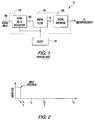
- Figure 1 illustrates a sigma delta converter 10, to which an analog signal 100 is fed into the device.
- the signal is compared in the modulator 110 to a referenced level that converges on the analog signal 100 in a closed feedback loop to produce a one-bit data stream 120 representing the analog amplitude.
- the one-bit data stream 120 then goes into a digital filter 130 to remove quantization noise and other internally generated noise.
- proper selection of a clock 140 will also allow the notch of the digital filter 130 to be at the line noise frequency (50 or 60 Hz) and allow suppression of common AC line noise picked up through inductive and capacitive coupling.
- the digital filter takes the 1-bit input data stream at a high sampling rate and decimates it to an N-bit data stream at a lower sampling rate.
- a digital interface 150 then provides the output of the digital filter 130 to a microprocessor or microcontroller.
- the theory of operation of a sigma delta converter 10 is well known.
- an input signal is sampled at a frequency many times higher than the highest input frequency of interest using a simple 1-bit comparator in a feedback loop.
- the quantization noise is broadband white noise in nature, however, it is shaped by the integration performed in the modulator so that the noise floor is much lower at lower frequencies and greater at higher frequencies out of the range of interest.
- the digital filter 130 then filters out this higher frequency noise allowing greater signal resolution at the low frequencies that are of interest.
- the actual signal-to-noise ratio and distortion specifications are a function of both the oversampling rate and the order of the integration in the modulator.
- the resolution of the converter can be increased by greater oversampling since the resultant quantization noise is spread over a wider bandwidth, and, even without the effect of noise shaping, each doubling of the sample rate theoretically yields a 3 dB dynamic range improvement.
- Modulator noise shaping depends upon the order of the modulator. For a second order modulator one would expect a theoretical dynamic range improvement of 15 dB for every doubling of the sample rate.
- the typical frequency spectrum of existing sigma delta converters for low frequency measurement applications is shown in FIG. 2 with a modulator sampling rate of fm, the usable bandwidth of the 1-bit sigma delta comparator is fm/2 based on the Nyquist Sampling theorem.
- the effective sampling rate, fs represents that frequency that provides the desired resolution for the maximum input signal of interest if the signal were sampled with more conventional means, such as a common successive approximation register (SAR) converter.
- the input signal bandwidth, fb defines the usable range of the converter over which there must be minimal signal attenuation from the filter (fb is commonly taken as the - 3 dB down point).
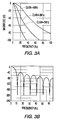
- FIG. 3A a finite impulse response (FIR) filter is shown with a sharp rolloff characteristic.
- This filter is used in the Crystal Semiconductor CS5501 sigma delta A/D converter, and fb is approximately 10 Hz when the clock crystal is 4.096 MHz. With this clock rate, the CS5501 filter provides approximately 55 dB rejection at 60 Hz to signals coming in to either the data input or reference voltage pins. With fb at 5 Hz, 60 Hz rejection increases to more than 90 dB.
- FIG. 3B the filter characteristics of the Analog Devices AD7712 are shown.
- the AD7712 uses a (sin x/x) 3 or sinc 3 comb filter to achieve acceptable fb and 60 Hz noise rejection with a simple implementation.
- the rejection of AC line noise can be very high. See U.S. Patent No. 5,349,352.
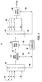
- FIG. 4 shows a preferred embodiment sigma delta converter 20 with input signals 200 fed into a multiplexer 205 for selection.
- the modulator 210 provides a one-bit digital data stream 220 representing the amplitude of the selected signal to the digital filter 230.
- the digital filter 230 in this architecture is designed to only filter out quantization and other relatively higher frequency (100 Hz or more) internally generated noise.
- the output of the digital filter 230 is then put into multiplexer 240 to feed a bank of data channel registers 250 where the data from the last 4N conversions of individual channels is accumulated. Data for each channel is averaged to remove AC line noise on a per channel basis, and the final digital signal, thus filtered for both external and internal noise, is made available to a microprocessor through the digital interface 260.
- the controller 280 outputs a control signal onto control bus 281 for input to the multiplexer 205 via multiplexer input control line 282.
- the control signal on control line 282 will indicate which of the external channels X1-XN are to be selected for conversion.
- the number of selected external channels will be less than the number of internal channels. Referring to Table 1, depending on the number of external channels selected, the external channel may be selected for conversion one or more times during a given quarter mains cycle. So, if N set is selected to be 6, then each selected external channel will be converted twice during each quarter mains cycle to provide moving average of 8 samples and a throughput of 480 Hz.
- each channel must be converted twice during a quarter mains cycle.
- seven (7) time slots are allocated to one external channel.
- the external channel will be sampled 7 times during each quarter mains cycle, there are four quarter mains cycles so the moving average is 28 and the throughput is 1,680 Hz.
- the number of time slots can be selected as well as the number of external channels.
- FIG. 5 shows a second preferred embodiment of an 8-channel multiplexed sigma delta converter 800 in simplified block form. Elements common to converters 20 and 800 have the same reference numerals as elements of FIG. 4; note that multiplexer 240 of FIG. 4 appears in calibration and averaging processor 241 of FIG. 5.
- the converter of FIG.5 sequentially samples each of the 8 inputs for durations of about 625 microseconds for 50 Hz line noise or 520 microseconds for 60 Hz line noise. This yields 500 or more samples per channel to compute each one of the outputs of filter 230 to average in processor 241 when the sampling frequency of modulator 210 is 1 MHz.
- filter 230 has decimated the sampling rate by a factor of 500 (from 1 MHz to 2000 Hz) because filter 230 only provides one output for every 500 data sample inputs.
- the multibit output may be conveniently offset and scaled prior to output. For example, with positive and negative inputs, two's complement output format may be convenient.
- Such calibration is programmed through interface 260 to load calibration values in registers 270.
- Processor 241 uses the calibration values in registers 270 to calibrate in addition to computing the averages.
- the electronics and fabrication are substantially simplified, compared to Converter 20 of Fig. 4, by manufacturing the A/D converter 800 with a fixed or predetermined number of time slots and a selectable or programmable number of external channels. So, turning to FIG. 5, there are eight (8) time slots, each formed by a first-in-first-out register in a register stack 250. During a conversion scan any selected number of the eight time slots may be converted. So, in order to control the throughput, the timing and control device 300 selects a binary integral number of external channels X1-X8. In other words, the timing control device 300 will select 8, 4, 2, or 1 external channels. Conversion will be accomplished in accordance with Tables 2-5.
- each external channel will be converted during a conversion scan and its conversion results will be stored as a digital value in one of the FIFO registers in stack 250.
- the four (4) channels will be sampled twice during a conversion scan.
- the results for one channel will be stored in FIFO register 1 and 5
- the results for a second channel will be stored in FIFO register 2 and 6, etc.
- Corresponding samplings and storings for two selected channels and one selected channel will be made as shown, respectively, in Tables 4 and 5.
- a user selects the number of input channels for conversion and enters the selection via the synchronous serial interface port 260 or other suitable input means.
- the selected input channels are converted from analog values to digital values during the eight respective time slots.
- the converted digital values are stored in the FIFO registers on register stack 250.
- the sequence in which the selected input channels are converted is also programmable.
- FIG. 6 schematically shows a second order modulator 210 and filter 230 for use in the converter of FIG. 5.
- the second order modulator 210 and filter 230 were derived from the specificaiton of U.S. Patent No. 5,345,236 Note that the clock and reset circuitry has been omitted from FIG. 6 for clarity.
- Modulator 210 in FIG. 6 operates as follows. At each clock period analog summing junction 611 adds input signal Vin to the negative of the output of digital-to-analog converter (DAC) 612. DAC 612 is a 1-bit converter and outputs either + Vref or - Vref.
- Analog integrator 613 adds the output of summing junction 611 to its current sum and outputs the new sum to summing junction 614.
- Summing junction 614 adds the sum from integrator 613 to the negative of the output of DAC 615 which duplicates the output of DAC 612.
- Analog integrator 616 adds the output of junction 614 to its current sum and outputs its new sum to comparator 617.
- Comparator 617 compares the sum to analog 0.0 and outputs a digital + 1 if the sum is nonnegative and outputs a digital - 1 if the sum is negative. (Comparator 617 could output + 1 and 0 and processor 241 will provide the compensation for the average being 1/2 rather than 0.)
- the output of comparator 617 feeds back to drive DAC 612 and DAC 615. This negative feedback keeps the magnitudes of the analog sums in integrators 613 and 616 to less than 2 Vref. Note that only analog integrators and digital accumulators are used, and the filter has no multiplications and no stored coefficients to be read from memory.
- the output of comparator 617 is filtered by digital filter 230 which includes inverter 621 feeding digital accumulator 622 and digital summing junction 623 combining the output of accumulator 622 and comparator 617 to be accumulated by output digital accumulator 624.
- the sum in accumulator 622 lies in the range of - M to + M after M clock periods from a reset, and thus the output to summing junction 623 is multi-bit.
- the sum in accumulator 624 lies in the range of - M(M - 1)/2 and + M(M - 1)/2 alter M clock periods from a reset.
- integrators 613 and 616 may have their gains scaled for convenience, and in this case the accumulators 622 and 624 should have corresponding scaling.
- a gain of 1/2 for each of integrators 613 and 616 is convenient.
- the magnitude of Vin is taken to be in the range - Vref/2 to + Vref/2 with Vref a reference voltage.
- the two digital accumulators of filter 230 correspond to the two analog integrators in modulator 210, and filter 230 runs "in parallel" with modulator 210.
- Vin is essentially constant during the M clock periods if the total integrating and accumulating time is small, for example 500 microseconds, because Vin is slowly varying but with 60 Hz noise.
- Vin(k) factors out of the summations, and the sum in integrator 616 then can be expressed in terms of the sum in accumulator 624 as VinM(M - 1)/2 + D(M)Vref
- the sum in integrator 616 has a magnitude of at most 2 Vref due to the negative feedback, and M(M - 1)/2 is growing as M 2 , thus D(M) is also growing as M 2 and Vin is approximated by - D(M)Vref/[M(M - 1)/2] .
- the sum in integrator 616 essentially is the approximation error, which is just the quantization noise.
- the approximation error has relative magnitude decreasing like M -2 .
- This means 16-bit resolution requires M to be roughly 2 8 - 2 9 which implies 256-512 samples; of course, including the integrator gain factors will change this somewhat.
- the 256-512 samples can be taken in 100 microseconds. This permits generation of 20 filtered output samples from each of the 8 channels during one period of the 60 Hz line frequency.
- processor 241 could insure rejection of 60 Hz line noise plus several higher harmonics by averaging 20 filter outputs.
- more channels or higher resolution could be used with an averaging of only 4 samples by processor 241.
- higher order modulators and filters such as three analog integrators in series in modulator 210 plus three corresponding digital accumulators in filter 230, can provide higher resolution. And the same analysis applies for a 50 Hz power line frequency.
- A/D 20 or 800 with eight input channels each coupled to a separate time slot one can achieve an increase in throughput of 4x the line frequency since 4 samples/channel are taken for each cycle of the line frequency i.e. one channel sample is taken during each quarter mains cycle (see FIG. 7).
- This invention provides a way of improving throughput so that more samples/channel can be taken while maintaining line rejection.
- One method converts the channels sequentially with the first channel of the set synchronized to the start of each quarter mains cycle (see FIG. 9). Note that the number of channels in the set (N set ) may be less than the maximum number of channels that can fit within one quarter mains cycle. This method works but limits each channel throughput to be 4x mains frequency independent of the number of channels used (N ch ).
- This invention increases the channel throughput by reducing N set and synchronizing the first channel of the set with respect to the start of an integral fraction of quarter mains cycle. For example, to increase the throughput of each channel by Nx, then the first channel in the set must be synchronized to the start of 1/N of quarter mains cycle. The moving average of the last 4N samples constitutes the output with line noise rejection.
- N set decreases because the number of channels that can fit within 1/N of quarter mains cycle decreases (see FIG. 10).
- Note that synchronization is required to maintain uniform time sampling. In a hardware implementation this can be quite involved as there is a need to keep track of N and N set and adjust the channel sample timing and moving average divisor accordingly.
- the general implementation of the invention is simplified by noting that there is no real need to take the moving average of the last 4N samples in high throughput mode.
- most A/D applications do not require use of all input channels and further noting that most A/D converters (including converters 20, 800) have eight input channels. From the time relationship of the samples one may continue to use an average of the last 4 corresponding samples (see FIG. 11). These corresponding channel samples are obtained by skipping the next (N-1) channel samples. In this case the converter will produce a stream of high throughput line rejected channel samples and the user picks the appropriate output samples corresponding to each channel.
- the advantage of this implementation is that the same hardware and timing is used independent of the throughput increase mode. This is illustrated in the following tables. Note that one does not connect the external channels to multiple internal channels as the internal channel differences will cause inaccuracies.
- the tables basically indicate how the internal channel time slots are utilized and if channel 1 is allotted to slots 1 and 5 (as in Table 3) then the same channel 1 connection is used.
- a sigma delta convertor 20 has a number of time slots that are programmable connectable to the input channels 200 via a multiplexer 205. Conversion throughput of any one input channel is increased by connecting two or more time slots to the input channel. For an eight input channel embodiment 800 the throughput of conversion of one input can be increased 2x, 4x or 8x by connecting, respectively, 2, 4 or all 8 time slots to the selected input channel.
Landscapes
- Engineering & Computer Science (AREA)
- Theoretical Computer Science (AREA)
- Compression, Expansion, Code Conversion, And Decoders (AREA)
- Analogue/Digital Conversion (AREA)
Applications Claiming Priority (2)
| Application Number | Priority Date | Filing Date | Title |
|---|---|---|---|
| US08/438,251 US5617090A (en) | 1995-05-10 | 1995-05-10 | Multi-channel sigma-delta A/D converters with improved throughput |
| US438251 | 1995-05-10 |
Publications (2)
| Publication Number | Publication Date |
|---|---|
| EP0742645A2 true EP0742645A2 (de) | 1996-11-13 |
| EP0742645A3 EP0742645A3 (de) | 1998-04-01 |
Family
ID=23739879
Family Applications (1)
| Application Number | Title | Priority Date | Filing Date |
|---|---|---|---|
| EP96106368A Withdrawn EP0742645A3 (de) | 1995-05-10 | 1996-04-23 | Mehrkanal-Sigma-Delta-Analog-Digital-Wandler mit hohem Durchsatz |
Country Status (4)
| Country | Link |
|---|---|
| US (1) | US5617090A (de) |
| EP (1) | EP0742645A3 (de) |
| JP (1) | JPH08330969A (de) |
| KR (1) | KR960043545A (de) |
Cited By (2)
| Publication number | Priority date | Publication date | Assignee | Title |
|---|---|---|---|---|
| WO2004030222A1 (en) * | 2002-09-27 | 2004-04-08 | Freescale Semiconductor, Inc. | Method and apparatus for shared processing a plurality of signals |
| WO2007144827A3 (en) * | 2006-06-15 | 2008-04-24 | Koninkl Philips Electronics Nv | A method of digitizing a periodic analogue signal. |
Families Citing this family (30)
| Publication number | Priority date | Publication date | Assignee | Title |
|---|---|---|---|---|
| JPH09297658A (ja) * | 1996-05-08 | 1997-11-18 | Mitsubishi Electric Corp | A/d変換装置 |
| WO2000013319A1 (en) * | 1998-08-26 | 2000-03-09 | The Johns Hopkins University | Remote input/output (rio) smart sensor analog-digital chip |
| US6177893B1 (en) * | 1998-09-15 | 2001-01-23 | Scott R. Velazquez | Parallel processing analog and digital converter |
| JP2002540710A (ja) * | 1999-03-26 | 2002-11-26 | コーニンクレッカ フィリップス エレクトロニクス エヌ ヴィ | 変換器 |
| EP1052800B1 (de) * | 1999-05-11 | 2006-09-20 | Koninklijke Philips Electronics N.V. | Übertragungssystem und Empfänger mit Vorrichtung zur Dezimation |
| US6791404B1 (en) | 1999-07-01 | 2004-09-14 | Broadcom Corporation | Method and apparatus for efficient mixed signal processing in a digital amplifier |
| US6466615B1 (en) * | 1999-12-30 | 2002-10-15 | Intel Corporation | Delay locked loop based circuit for data communication |
| US6426713B1 (en) * | 2000-07-05 | 2002-07-30 | Cirrus Logic, Inc. | Independent control of calibration registers in a multi channel A-D converter |
| US6593865B2 (en) | 2001-08-15 | 2003-07-15 | Analog Devices, Inc. | Rapid multiplexing analog to digital converter |
| US20030076250A1 (en) * | 2001-10-19 | 2003-04-24 | Enochson Mark P. | Method and apparatus for flexible analog-to-digital conversion |
| EP1504530A4 (de) * | 2002-04-10 | 2008-11-05 | Systel Dev And Ind Ltd | System auf einem chip zur digitalen steuerung elektronischer leistungseinrichtungen |
| US6768441B2 (en) * | 2002-08-20 | 2004-07-27 | Telefonaktiebolaget L.M. Ericsson | Methods of receiving communications signals including a plurality of digital filters having different bandwidths and related receivers |
| US6924755B1 (en) * | 2002-12-02 | 2005-08-02 | Analog Devices, Inc. | Multi-channel analog to digital converter which facilitates calibration of the analog to digital converter and respective input channels to the analog to digital converter, and a method for calibrating the analog to digital converter |
| WO2004054113A1 (en) * | 2002-12-09 | 2004-06-24 | Analog Devices Inc. | An integraded circuit comprising a dac with provision for setting the dac to a clear condition, and a method for setting a dac to a clear condition |
| US7340230B2 (en) * | 2003-04-14 | 2008-03-04 | Silicon Laboratories Inc. | Receiver architectures utilizing coarse analog tuning and associated methods |
| US20040205827A1 (en) * | 2003-04-14 | 2004-10-14 | Krone Andrew W. | Multi-stage channel select filter and associated method |
| US6819274B2 (en) * | 2003-04-14 | 2004-11-16 | Silicon Laboratories Inc. | Method for tuning a bandpass analog-to-digital converter and associated architecture |
| US7049987B2 (en) * | 2003-08-12 | 2006-05-23 | Siemens Building Technologies Ag | Arrangement for generating a clock signal for a sigma-delta analog-to-digital converter |
| US6950044B1 (en) * | 2004-03-31 | 2005-09-27 | Silicon Labs Cp, Inc. | Mixed signal processor with noise management |
| JP2005333258A (ja) * | 2004-05-18 | 2005-12-02 | Fujitsu Ltd | アナログ/デジタル変換装置 |
| US7413342B2 (en) * | 2005-02-22 | 2008-08-19 | Micron Technology, Inc. | DRAM temperature measurement system |
| US7738951B2 (en) * | 2006-07-28 | 2010-06-15 | Medtronic, Inc. | Prioritized multicomplexor sensing circuit |
| FI124317B (fi) * | 2007-02-12 | 2014-06-30 | Abb Oy | Sähkömoottorikäyttö |
| US7504977B2 (en) * | 2007-04-23 | 2009-03-17 | Texas Instruments Incorporated | Hybrid delta-sigma/SAR analog to digital converter and methods for using such |
| WO2009042137A2 (en) * | 2007-09-25 | 2009-04-02 | Lam Research Corporation | Temperature control modules for showerhead electrode assemblies for plasma processing apparatuses |
| US8237598B2 (en) * | 2010-07-30 | 2012-08-07 | National Instruments Corporation | Sampling of multiple data channels using a successive approximation register converter |
| FR3016056B1 (fr) | 2013-12-31 | 2017-05-05 | Commissariat Energie Atomique | Systeme d'acquisition d'images par holographie numerique heterodyne |
| JP6769453B2 (ja) * | 2018-03-22 | 2020-10-14 | カシオ計算機株式会社 | A/d変換装置、a/d変換方法及びプログラム |
| FR3097337B1 (fr) * | 2019-06-13 | 2021-07-23 | Commissariat Energie Atomique | Système d’imagerie acousto-optique |
| US11496133B1 (en) * | 2021-07-29 | 2022-11-08 | United States Of America As Represented By The Administrator Of Nasa | Radiation hardened housekeeping slave node (RH-HKSN) application specific integrated circuit (ASIC) element |
Family Cites Families (7)
| Publication number | Priority date | Publication date | Assignee | Title |
|---|---|---|---|---|
| US4564831A (en) * | 1982-07-02 | 1986-01-14 | Transamerica Delaval Inc. | Analog to digital converters for converting a plurality of different input signals |
| US5043911A (en) * | 1989-12-22 | 1991-08-27 | Sundstrand Corporation | Multiplexing A/D converter for a generator control unit |
| IE901815A1 (en) * | 1990-05-21 | 1991-12-04 | Univ Cork | An analog to digital converter |
| JP2553753B2 (ja) * | 1990-10-17 | 1996-11-13 | 三菱電機株式会社 | Ad変換装置 |
| US5248971A (en) * | 1992-05-19 | 1993-09-28 | Mandl William J | Method and apparatus for multiplexed oversampled analog to digital modulation |
| US5345236A (en) * | 1992-12-21 | 1994-09-06 | Harris Corporation | Improved sigma-delta type analog-to-digital converter and method |
| US5349352A (en) * | 1992-12-21 | 1994-09-20 | Harris Corporation | Analog-to-digital converter having high AC line noise rejection and insensitive to AC line frequency variations |
-
1995
- 1995-05-10 US US08/438,251 patent/US5617090A/en not_active Expired - Lifetime
-
1996
- 1996-04-23 EP EP96106368A patent/EP0742645A3/de not_active Withdrawn
- 1996-05-04 KR KR1019960014587A patent/KR960043545A/ko not_active Ceased
- 1996-05-09 JP JP8115039A patent/JPH08330969A/ja not_active Withdrawn
Cited By (3)
| Publication number | Priority date | Publication date | Assignee | Title |
|---|---|---|---|---|
| WO2004030222A1 (en) * | 2002-09-27 | 2004-04-08 | Freescale Semiconductor, Inc. | Method and apparatus for shared processing a plurality of signals |
| US7142606B2 (en) | 2002-09-27 | 2006-11-28 | Freescale Semiconductor, Inc. | Method and apparatus for shared processing a plurality of signals |
| WO2007144827A3 (en) * | 2006-06-15 | 2008-04-24 | Koninkl Philips Electronics Nv | A method of digitizing a periodic analogue signal. |
Also Published As
| Publication number | Publication date |
|---|---|
| JPH08330969A (ja) | 1996-12-13 |
| KR960043545A (ko) | 1996-12-23 |
| EP0742645A3 (de) | 1998-04-01 |
| US5617090A (en) | 1997-04-01 |
Similar Documents
| Publication | Publication Date | Title |
|---|---|---|
| EP0742645A2 (de) | Mehrkanal-Sigma-Delta-Analog-Digital-Wandler mit hohem Durchsatz | |
| US5345236A (en) | Improved sigma-delta type analog-to-digital converter and method | |
| US5124705A (en) | Analog-to-digital signal converter comprising a multiple sigma-delta modulator | |
| US5134401A (en) | Delta sigma modulator having programmable gain/attenuation | |
| Carley et al. | A 16-bit 4'th order noise-shaping D/A converter | |
| US5627536A (en) | Multiplexed delta-sigma modulator | |
| US6035320A (en) | Fir filter architecture | |
| US5055843A (en) | Sigma delta modulator with distributed prefiltering and feedback | |
| EP0586021B1 (de) | Digitale Rauschformerschaltung | |
| US6346898B1 (en) | Multilevel analog to digital data converter having dynamic element matching in a reference data path | |
| US5412387A (en) | Error reduction in switched capacitor digital-to-analog converter systems by balanced sampling | |
| US6922161B2 (en) | Delta-Sigma modulator for reducing quantization noise and oversampling ratio (OSR) | |
| US7450046B2 (en) | Delta-sigma modulator and A/D converter | |
| US5561660A (en) | Offset and phase correction for delta-sigma modulators | |
| EP0643488A1 (de) | Sigma-Delta Analog-Digital Konverter mit einem Filter mit definierter Nullstellen-Pol-Verteilung und Gerät dafür | |
| TWI496421B (zh) | 類比/數位轉換器 | |
| JP2000509927A (ja) | スイッチ電流デルタ・シグマ変調器 | |
| GB2080059A (en) | Digital-to-analogue converter | |
| EP0790708A2 (de) | Interpolierende Digital-Analog-Wandler-Architektur zur verbesserten Störsignalunterdrückung | |
| WO2004049561A1 (en) | Pulse width-modulated noise shaper | |
| US20020175671A1 (en) | Apparatus and system for electrical power metering using digital integration | |
| EP0778676A2 (de) | Vielfach-Abtastraten-Digitalfilter und Verfahren für einen sigma-delta Konversionsprozess | |
| KR100338971B1 (ko) | 선택가능한데시메이션비율을제공하기위해영충전회로를이용한필터 | |
| EP0229764B1 (de) | Interpolierender analog-digital-wandler | |
| US5446917A (en) | Programmable length decimation filter as for sigma-delta modulators |
Legal Events
| Date | Code | Title | Description |
|---|---|---|---|
| PUAI | Public reference made under article 153(3) epc to a published international application that has entered the european phase |
Free format text: ORIGINAL CODE: 0009012 |
|
| AK | Designated contracting states |
Kind code of ref document: A2 Designated state(s): DE FR GB IT SE |
|
| PUAL | Search report despatched |
Free format text: ORIGINAL CODE: 0009013 |
|
| AK | Designated contracting states |
Kind code of ref document: A3 Designated state(s): DE FR GB IT SE |
|
| 17P | Request for examination filed |
Effective date: 19980916 |
|
| 17Q | First examination report despatched |
Effective date: 20010921 |
|
| GRAH | Despatch of communication of intention to grant a patent |
Free format text: ORIGINAL CODE: EPIDOS IGRA |
|
| STAA | Information on the status of an ep patent application or granted ep patent |
Free format text: STATUS: THE APPLICATION IS DEEMED TO BE WITHDRAWN |
|
| 18D | Application deemed to be withdrawn |
Effective date: 20030905 |