EP0743686A2 - Vorprodukt für Halbleiterdünnschichten und Verfahren zur Herstellung von Halbleiterdünnschichten - Google Patents
Vorprodukt für Halbleiterdünnschichten und Verfahren zur Herstellung von Halbleiterdünnschichten Download PDFInfo
- Publication number
- EP0743686A2 EP0743686A2 EP96107692A EP96107692A EP0743686A2 EP 0743686 A2 EP0743686 A2 EP 0743686A2 EP 96107692 A EP96107692 A EP 96107692A EP 96107692 A EP96107692 A EP 96107692A EP 0743686 A2 EP0743686 A2 EP 0743686A2
- Authority
- EP
- European Patent Office
- Prior art keywords
- thin film
- film
- semiconductor thin
- manufacturing
- precursor
- Prior art date
- Legal status (The legal status is an assumption and is not a legal conclusion. Google has not performed a legal analysis and makes no representation as to the accuracy of the status listed.)
- Withdrawn
Links
Images


Classifications
-
- C—CHEMISTRY; METALLURGY
- C23—COATING METALLIC MATERIAL; COATING MATERIAL WITH METALLIC MATERIAL; CHEMICAL SURFACE TREATMENT; DIFFUSION TREATMENT OF METALLIC MATERIAL; COATING BY VACUUM EVAPORATION, BY SPUTTERING, BY ION IMPLANTATION OR BY CHEMICAL VAPOUR DEPOSITION, IN GENERAL; INHIBITING CORROSION OF METALLIC MATERIAL OR INCRUSTATION IN GENERAL
- C23C—COATING METALLIC MATERIAL; COATING MATERIAL WITH METALLIC MATERIAL; SURFACE TREATMENT OF METALLIC MATERIAL BY DIFFUSION INTO THE SURFACE, BY CHEMICAL CONVERSION OR SUBSTITUTION; COATING BY VACUUM EVAPORATION, BY SPUTTERING, BY ION IMPLANTATION OR BY CHEMICAL VAPOUR DEPOSITION, IN GENERAL
- C23C14/00—Coating by vacuum evaporation, by sputtering or by ion implantation of the coating forming material
- C23C14/58—After-treatment
- C23C14/5846—Reactive treatment
- C23C14/5866—Treatment with sulfur, selenium or tellurium
-
- C—CHEMISTRY; METALLURGY
- C23—COATING METALLIC MATERIAL; COATING MATERIAL WITH METALLIC MATERIAL; CHEMICAL SURFACE TREATMENT; DIFFUSION TREATMENT OF METALLIC MATERIAL; COATING BY VACUUM EVAPORATION, BY SPUTTERING, BY ION IMPLANTATION OR BY CHEMICAL VAPOUR DEPOSITION, IN GENERAL; INHIBITING CORROSION OF METALLIC MATERIAL OR INCRUSTATION IN GENERAL
- C23C—COATING METALLIC MATERIAL; COATING MATERIAL WITH METALLIC MATERIAL; SURFACE TREATMENT OF METALLIC MATERIAL BY DIFFUSION INTO THE SURFACE, BY CHEMICAL CONVERSION OR SUBSTITUTION; COATING BY VACUUM EVAPORATION, BY SPUTTERING, BY ION IMPLANTATION OR BY CHEMICAL VAPOUR DEPOSITION, IN GENERAL
- C23C14/00—Coating by vacuum evaporation, by sputtering or by ion implantation of the coating forming material
- C23C14/06—Coating by vacuum evaporation, by sputtering or by ion implantation of the coating forming material characterised by the coating material
- C23C14/0623—Sulfides, selenides or tellurides
-
- C—CHEMISTRY; METALLURGY
- C23—COATING METALLIC MATERIAL; COATING MATERIAL WITH METALLIC MATERIAL; CHEMICAL SURFACE TREATMENT; DIFFUSION TREATMENT OF METALLIC MATERIAL; COATING BY VACUUM EVAPORATION, BY SPUTTERING, BY ION IMPLANTATION OR BY CHEMICAL VAPOUR DEPOSITION, IN GENERAL; INHIBITING CORROSION OF METALLIC MATERIAL OR INCRUSTATION IN GENERAL
- C23C—COATING METALLIC MATERIAL; COATING MATERIAL WITH METALLIC MATERIAL; SURFACE TREATMENT OF METALLIC MATERIAL BY DIFFUSION INTO THE SURFACE, BY CHEMICAL CONVERSION OR SUBSTITUTION; COATING BY VACUUM EVAPORATION, BY SPUTTERING, BY ION IMPLANTATION OR BY CHEMICAL VAPOUR DEPOSITION, IN GENERAL
- C23C14/00—Coating by vacuum evaporation, by sputtering or by ion implantation of the coating forming material
- C23C14/06—Coating by vacuum evaporation, by sputtering or by ion implantation of the coating forming material characterised by the coating material
- C23C14/08—Oxides
-
- H—ELECTRICITY
- H10—SEMICONDUCTOR DEVICES; ELECTRIC SOLID-STATE DEVICES NOT OTHERWISE PROVIDED FOR
- H10F—INORGANIC SEMICONDUCTOR DEVICES SENSITIVE TO INFRARED RADIATION, LIGHT, ELECTROMAGNETIC RADIATION OF SHORTER WAVELENGTH OR CORPUSCULAR RADIATION
- H10F10/00—Individual photovoltaic cells, e.g. solar cells
- H10F10/10—Individual photovoltaic cells, e.g. solar cells having potential barriers
- H10F10/16—Photovoltaic cells having only PN heterojunction potential barriers
- H10F10/167—Photovoltaic cells having only PN heterojunction potential barriers comprising Group I-III-VI materials, e.g. CdS/CuInSe2 [CIS] heterojunction photovoltaic cells
-
- H—ELECTRICITY
- H10—SEMICONDUCTOR DEVICES; ELECTRIC SOLID-STATE DEVICES NOT OTHERWISE PROVIDED FOR
- H10F—INORGANIC SEMICONDUCTOR DEVICES SENSITIVE TO INFRARED RADIATION, LIGHT, ELECTROMAGNETIC RADIATION OF SHORTER WAVELENGTH OR CORPUSCULAR RADIATION
- H10F77/00—Constructional details of devices covered by this subclass
- H10F77/10—Semiconductor bodies
- H10F77/12—Active materials
- H10F77/126—Active materials comprising only Group I-III-VI chalcopyrite materials, e.g. CuInSe2, CuGaSe2 or CuInGaSe2 [CIGS]
- H10F77/1265—Active materials comprising only Group I-III-VI chalcopyrite materials, e.g. CuInSe2, CuGaSe2 or CuInGaSe2 [CIGS] characterised by the dopants
-
- Y—GENERAL TAGGING OF NEW TECHNOLOGICAL DEVELOPMENTS; GENERAL TAGGING OF CROSS-SECTIONAL TECHNOLOGIES SPANNING OVER SEVERAL SECTIONS OF THE IPC; TECHNICAL SUBJECTS COVERED BY FORMER USPC CROSS-REFERENCE ART COLLECTIONS [XRACs] AND DIGESTS
- Y02—TECHNOLOGIES OR APPLICATIONS FOR MITIGATION OR ADAPTATION AGAINST CLIMATE CHANGE
- Y02E—REDUCTION OF GREENHOUSE GAS [GHG] EMISSIONS, RELATED TO ENERGY GENERATION, TRANSMISSION OR DISTRIBUTION
- Y02E10/00—Energy generation through renewable energy sources
- Y02E10/50—Photovoltaic [PV] energy
- Y02E10/541—CuInSe2 material PV cells
-
- Y—GENERAL TAGGING OF NEW TECHNOLOGICAL DEVELOPMENTS; GENERAL TAGGING OF CROSS-SECTIONAL TECHNOLOGIES SPANNING OVER SEVERAL SECTIONS OF THE IPC; TECHNICAL SUBJECTS COVERED BY FORMER USPC CROSS-REFERENCE ART COLLECTIONS [XRACs] AND DIGESTS
- Y02—TECHNOLOGIES OR APPLICATIONS FOR MITIGATION OR ADAPTATION AGAINST CLIMATE CHANGE
- Y02P—CLIMATE CHANGE MITIGATION TECHNOLOGIES IN THE PRODUCTION OR PROCESSING OF GOODS
- Y02P70/00—Climate change mitigation technologies in the production process for final industrial or consumer products
- Y02P70/50—Manufacturing or production processes characterised by the final manufactured product
-
- Y—GENERAL TAGGING OF NEW TECHNOLOGICAL DEVELOPMENTS; GENERAL TAGGING OF CROSS-SECTIONAL TECHNOLOGIES SPANNING OVER SEVERAL SECTIONS OF THE IPC; TECHNICAL SUBJECTS COVERED BY FORMER USPC CROSS-REFERENCE ART COLLECTIONS [XRACs] AND DIGESTS
- Y10—TECHNICAL SUBJECTS COVERED BY FORMER USPC
- Y10S—TECHNICAL SUBJECTS COVERED BY FORMER USPC CROSS-REFERENCE ART COLLECTIONS [XRACs] AND DIGESTS
- Y10S438/00—Semiconductor device manufacturing: process
- Y10S438/93—Ternary or quaternary semiconductor comprised of elements from three different groups, e.g. I-III-V
-
- Y—GENERAL TAGGING OF NEW TECHNOLOGICAL DEVELOPMENTS; GENERAL TAGGING OF CROSS-SECTIONAL TECHNOLOGIES SPANNING OVER SEVERAL SECTIONS OF THE IPC; TECHNICAL SUBJECTS COVERED BY FORMER USPC CROSS-REFERENCE ART COLLECTIONS [XRACs] AND DIGESTS
- Y10—TECHNICAL SUBJECTS COVERED BY FORMER USPC
- Y10T—TECHNICAL SUBJECTS COVERED BY FORMER US CLASSIFICATION
- Y10T428/00—Stock material or miscellaneous articles
- Y10T428/12—All metal or with adjacent metals
- Y10T428/12493—Composite; i.e., plural, adjacent, spatially distinct metal components [e.g., layers, joint, etc.]
- Y10T428/12528—Semiconductor component
-
- Y—GENERAL TAGGING OF NEW TECHNOLOGICAL DEVELOPMENTS; GENERAL TAGGING OF CROSS-SECTIONAL TECHNOLOGIES SPANNING OVER SEVERAL SECTIONS OF THE IPC; TECHNICAL SUBJECTS COVERED BY FORMER USPC CROSS-REFERENCE ART COLLECTIONS [XRACs] AND DIGESTS
- Y10—TECHNICAL SUBJECTS COVERED BY FORMER USPC
- Y10T—TECHNICAL SUBJECTS COVERED BY FORMER US CLASSIFICATION
- Y10T428/00—Stock material or miscellaneous articles
- Y10T428/12—All metal or with adjacent metals
- Y10T428/12493—Composite; i.e., plural, adjacent, spatially distinct metal components [e.g., layers, joint, etc.]
- Y10T428/12535—Composite; i.e., plural, adjacent, spatially distinct metal components [e.g., layers, joint, etc.] with additional, spatially distinct nonmetal component
- Y10T428/12611—Oxide-containing component
-
- Y—GENERAL TAGGING OF NEW TECHNOLOGICAL DEVELOPMENTS; GENERAL TAGGING OF CROSS-SECTIONAL TECHNOLOGIES SPANNING OVER SEVERAL SECTIONS OF THE IPC; TECHNICAL SUBJECTS COVERED BY FORMER USPC CROSS-REFERENCE ART COLLECTIONS [XRACs] AND DIGESTS
- Y10—TECHNICAL SUBJECTS COVERED BY FORMER USPC
- Y10T—TECHNICAL SUBJECTS COVERED BY FORMER US CLASSIFICATION
- Y10T428/00—Stock material or miscellaneous articles
- Y10T428/12—All metal or with adjacent metals
- Y10T428/12493—Composite; i.e., plural, adjacent, spatially distinct metal components [e.g., layers, joint, etc.]
- Y10T428/12681—Ga-, In-, Tl- or Group VA metal-base component
-
- Y—GENERAL TAGGING OF NEW TECHNOLOGICAL DEVELOPMENTS; GENERAL TAGGING OF CROSS-SECTIONAL TECHNOLOGIES SPANNING OVER SEVERAL SECTIONS OF THE IPC; TECHNICAL SUBJECTS COVERED BY FORMER USPC CROSS-REFERENCE ART COLLECTIONS [XRACs] AND DIGESTS
- Y10—TECHNICAL SUBJECTS COVERED BY FORMER USPC
- Y10T—TECHNICAL SUBJECTS COVERED BY FORMER US CLASSIFICATION
- Y10T428/00—Stock material or miscellaneous articles
- Y10T428/12—All metal or with adjacent metals
- Y10T428/12493—Composite; i.e., plural, adjacent, spatially distinct metal components [e.g., layers, joint, etc.]
- Y10T428/12771—Transition metal-base component
- Y10T428/12861—Group VIII or IB metal-base component
- Y10T428/12903—Cu-base component
Definitions
- This invention relates to a precursor for forming semiconductor thin films and a method for manufacturing semiconductor thin films using the precursor, and more particularly to a precursor for forming semiconductor thin films and a method for manufacturing semiconductor thin films suitable for a solar cell having a high energy conversion efficiency.
- a thin film solar cell using, for a photoabsorptive layer, a compound semiconductor thin film (a semiconductor thin film having a chalcopyrite structure) that comprises Ib-, IIIa- and VIa-group elements such as CuInSe 2 has high energy conversion efficiency and does not suffer from efficiency deterioration due to light irradiation or the like.
- a selenization method has been disclosed as a method for manufacturing a comparatively uniform CuInSe 2 thin film to fabricate a large area solar cell to be used as an energy source. According to the selenization method, a laminated thin film of Cu and In formed on a metallic film is sintered in an atmosphere containing H 2 Se and Se vapor so that the large area solar cell is fabricated.
- a method for doping a IIb-group element such as Zn or Cd has been known as a method for setting a semiconductor having a chalcopyrite structure including Ib-, IIIa- and VIa-group elements as an n type.
- Se which is the VIa-group element
- Cl which is a VIIa-group element
- An example of a parameter for determining the performance of the solar cell is a carrier concentration. If the carrier concentration is high, the diffusion potential of the pn junction becomes high so that an open circuit voltage (Voc) is increased. However, the width of a depletion layer whose carriers can be collected with few recombination thereof is reduced. Consequently, a short-circuit photocurrent is decreased. If the carrier concentration is low, the depletion layer width is increased. Consequently, the short circuit photocurrent is increased. However, since the diffusion potential is lowered, the open circuit voltage is reduced. Accordingly, there is a carrier concentration which is necessary for converting light to electrical energy most effectively. Furthermore, when the carrier concentration varies over the thickness of the film, an internal electric field is generated over the film.
- a forbidden band gap is about 1.0 eV, which is smaller than the forbidden band gap of the absorber layer having the highest conversion efficiency obtained from the matching with sunlight spectrum, i.e., about 1.4 eV.
- a solar cell using a Cu(In,Ga)Se 2 thin film having a forbidden band gap increased by forming a solid solution with Ga (a IIIa-group element) has been developed actively. As a method for enhancing the efficiency of the solar cell, the forbidden band gap of the absorber layer is gradually changed.
- the forbidden band gap is changed, an electric field is generated in the absorber layer so that the photo-excited carriers can be collected efficiently. Accordingly, a photocurrent is increased.
- a graded type Cu(In,Ga)Se 2 film has been studied.
- the composition ratio of Ga is varied in the direction of a film thickness of the absorber layer.
- elements Cu, In and Ga are mixed or stacked in the state of a metallic element with the desired composition. However, it is hard to control a diffusion speed in the metallic state.
- the objective composition is hard to obtain so that a layer having a composition ratio changed in the direction of a thickness thereof cannot be obtained with an objective composition ratio.
- the composition ratio is hard to control in case of mass production. Consequently, a constant quality cannot be obtained.
- the CuInS 2 and CuInSe 2 films which are made from Cu-In-O as a precursor by the sulfurization or selenization method have a little adhesion to a metallic film on the surface that is used as an electrode. Accordingly, it is preferred that the adhesion is increased to fabricate a solar cell having a stable conversion efficiency.
- the present invention provides a precursor for manufacturing a semiconductor thin film in which an oxide thin film comprising at least one element as a dopant selected from the group which consists of Ia-, IIa-, IIb-, Va- and Vb-group elements, and Ib- and IIIa-group elements as main components is deposited on a substrate.
- the oxide thin film comprising the dopant and Ib- and IIIa-group elements deposited on the substrate has the distribution in which the composition ratio with respect to the dopant is not constant from the substrate to the film surface in the direction of film thickness.
- the present invention provides a second precursor for manufacturing a semiconductor thin film in which at least two oxide thin films comprising an element as a dopant and Ib- and IIIa-group elements are deposited on a substrate, the oxide thin films having two or more layers in which the composition ratios with respect to the element as the dopant are different.
- the present invention provides a third precursor for manufacturing a semiconductor thin film, wherein at least one oxide thin film comprising Ib- and IIIa-group elements and at least one oxide thin film comprising an element as a dopant are alternately deposited on a substrate.
- an oxide thin film comprising the element as the dopant is deposited on the substrate and an oxide thin film comprising Ib- and IIIa-group elements is then deposited.
- the element as a dopant is the Ia-, Va- or Vb-group element and the substrate is a metal body or metal film
- the element as a dopant is the IIa- or IIb-group element and the substrate is a transparency conductive film
- the above embodiment is preferred.
- an oxide thin film comprising Ib- and IIIa-group elements is deposited on the substrate and an oxide thin film comprising an element as a dopant is then deposited.
- the element as a dopant is the Ia-, Va- or Vb-group element and the substrate comprises a transparent conductive film
- the above embodiment is preferred.
- the element as a dopant is the IIa- or IIb-group element and the substrate is a metal body or metal film
- the present embodiment is preferred.
- an oxide thin film comprising a first element as a dopant, an oxide thin film comprising Ib- and IIIa- group elements, and an oxide thin film comprising a second element as a dopant are sequentially deposited.
- oxide thin films comprising two kinds of dopants that supply holes and electrons are used.
- the present embodiment is effective for forming a pn homo-junction.
- the substrate is a transparent conductive film or a two-layered film comprising a transparent conductive film and a transparent insulating film
- the first element which acts as a dopant is at least one element selected from the group which consists of IIa- and IIb-group elements
- the second element which acts as a dopant is at least one element selected from the group which consists of Ia-, Va- and Vb-group elements.
- the present invention provides a precursor for manufacturing a semiconductor thin film in which an oxide thin film comprising Ib- and IIIa-group elements is deposited on a substrate, wherein the composition of at least one of the Ib- and IIIa-group elements is varied in the direction of film thickness.
- the oxide thin film comprising the Ib- and IIIa-group elements deposited on the substrate contains a Ib-group element and at least two kinds of IIIa-group elements, and the composition ratio of the IIIa-group elements is continuously varied from the substrate to the deposited oxide thin film surface in the direction of film thickness.
- the substrate is a metal substrate or an insulating substrate coated with a metal thin film.
- the heat treatment is performed in an atmosphere further containing at least one of hydrogen and carbon monoxide.
- the heat treatment is performed at a temperature of 200 to 1000°C .
- the semiconductor thin film is used for an absorber of a solar cell.
- Figs. 1 (a) and (b) show a part of a step of manufacturing a semiconductor thin film according to an embodiment of the present invention.
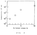
- Fig. 3 is a chart showing the change of the conductivity of a CuInSe 2 :Na film with change in the content of Na.
- Fig. 4 is a sectional view schematically showing a sputtering device for manufacturing an oxide precursor for the formation of a semiconductor thin film according to the embodiment of the present invention.
- Fig. 5 is a sectional view showing the structure of the precursor for producing a semiconductor thin film according to the embodiment of the present invention.
- Fig. 6 is a sectional view showing the structure of a precursor for producing a semiconductor thin film according to another embodiment of the present invention.
- Fig. 8 is a sectional view showing the structure of the precursor for producing a semiconductor thin film according to the embodiment of the present invention.
- Fig. 9 is a chart showing the voltage-current characteristic of the CuInS 2 film in which Mg and P are doped.
- Fig. 10 is a chart showing the X-ray diffraction pattern of the oxide precursor obtained according to an embodiment of the present invention.
- Fig. 11 is a chart showing the X-ray diffraction pattern of a Cu(In,Ga)Se 2 film obtained according to an embodiment of the present invention.
- Fig. 12 is a graph showing the composition distribution in the direction of the thickness of an oxide precursor film obtained according to one of the embodiments of the present invention.
- Fig. 13 is a graph showing the composition distribution in the direction of the thickness of the Cu(In,Ga)Se 2 film obtained according to one of the embodiments of the present invention.
- Fig. 14 is a schematically sectional view showing another sputtering device used for the manufacture of an oxide precursor film according to the embodiment of the present invention.
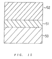
- Fig. 15 is a sectional view showing the structure of an oxide precursor film obtained according to another embodiment of the present invention.
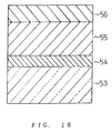
- Fig. 16 is a sectional view showing the structure of an oxide precursor film obtained according to still another embodiment of the present invention.
- Fig. 17 is a graph showing the composition distribution in the direction of the thickness of the oxide precursor film according to one of the embodiments of the present invention.
- Fig. 18 is a graph showing the composition distribution in the direction of the thickness of the Cu(In,Ga)Se 2 film obtained according to one of the embodiments of the present invention.
- a small amount of a Ia-, Va- or Vb-group element which acts as a p type dopant is added to, or an oxide film which comprises any of these elements is laminated on, an oxide thin film which comprises Ib- and IIIa group elements so that a precursor is formed. Then, the precursor is heat treated in an atmosphere which contains a VIa-group element. Thus, a semiconductor thin film having a chalcopyrite structure which comprises the Ib-, IIIa- and VIa-group elements is produced. At the step where the semiconductor thin film is formed, the element which acts as a dopant is incorporated into the semiconductor thin film. Consequently, it is possible to obtain a film, having very few defects and impurity phases that are different from the semiconductor, as a main product.
- doping can be performed on the semiconductor film effectively. It is effective to give the ununiform distribution of a carrier concentration to the semiconductor film in the thickness direction in order to enhance the efficiency of a solar cell.
- a pn junction in which an n type semiconductor film is formed on a p type semiconductor film having a chalcopyrite structure where the carrier concentration is increased in the vicinity of a metal that acts as an electrode and gradually decreased toward the film surface, an electric field is generated by the diffusion potential in a depletion layer area on a pn junction portion and an internal electric field is generated in the film due to a difference in carrier concentration.
- a small number of photo-excited carriers are moved by the internal electric field, collected on a pn junction face and fetched to the outside.
- a surface or back face an interface between a thin film and a substrate
- a surface or back face an interface between a thin film and a substrate
- the pn homo-junction can be formed.
- the Ia-, Va- or Vb-group element which acts as a p type dopant is combined, it is possible to form a pn junction in which the diffusion potential or depletion layer width is controlled.
- a precursor for manufacturing a semiconductor thin film and a method for manufacturing a semiconductor thin film according to the present invention wherein the distribution of a forbidden band gap is controlled will be described below.
- an oxide which comprises the Ib- and IIIa-group elements deposited on a substrate is an oxide thin film which contains the Ib-group element and at least two or more IIIa-group elements.
- the composition ratio of at least two or more IIIa-group elements is varied in the direction of film thickness, i.e., from the substrate to the deposited oxide thin film surface, so as to be continuously varied.
- a solar cell is fabricated by using the Cu(In,Ga)Se 2 film as a semiconductor thin film for an absorber, the carriers that are photo-excited in the vicinity of the electrode comprising a substrate are moved to the pn junction face by the internal electric field generated by the change of the forbidden band gap. Accordingly, the carriers can be taken out to the outside efficiently so that a photocurrent is increased. Also the precursor comprising multiple stacked oxide films which contain specific IIIa-group elements at different composition ratios described in a second embodiment of the present invention allows the change of the forbidden band gap to be implemented.
- the content rate of the Ib-group element is the same as that of the IIIa-group element in each layer, i.e., the ratio of numbers of atoms is 1 : 1 on each layer.
- the content rate of In as the specific IIIa-group element is 0.8 on a first layer and 1 on a second layer.
- each layer may include two or more kinds of IIIa-group elements.
- the content rate of the Ib-group element is the same as that of the IIIa-group element on each layer, i.e., the ratio of numbers of atoms is 1 : 1 on each layer.
- the content rate of In as the specific IIIa-group element is 0.6 on a first layer and 0.8 on a second layer. Such a case is included in the second embodiment.
- the composition ratio of the Ib-group element and the IIIa-group element of each oxide thin film is kept so that the forbidden band gap can be changed by a multi-layered film.
- the IIIa-group element includes at least Ga in the deposited oxide thin film comprising Ib- and IIIa-group elements that is in contact with the substrate side since a material such as CuGaSe 2 or CuGaS 2 has better adhesion than CuInSe 2 or CuInS 2 when a metal body or a metal film is used as a substrate. Accordingly, when a film that contains at least Ga, for example a Cu-Ga-O film or a Cu-In-Ga-O film is deposited on the substrate and sintered, a semiconductor thin film having a chalcopyrite structure which has excellent adhesion to the substrate can be obtained.
- the metal body substrate or metal thin film can be used as an electrode when forming a solar cell.
- the precursor according to the present embodiment can be used for a so-called substrate type solar cell which is used by irradiating light on the semiconductor thin film.
- a semiconductor thin film having a chalcopyrite structure is formed.
- the semiconductor thin film can be applied effectively to a superstrate type solar cell which develops electromotive force by irradiating sunlight on the transparent insulator face that is not coated with the transparent conductive film.
- a pn junction layer is formed in the vicinity of the substrate surface. Consequently, Ga is gradually increased from the substrate to the semiconductor thin film surface, conversely to the above-mentioned embodiment, so that an internal electric field which moves the photocarriers to the pn junction layer can be generated.
- a precursor for manufacturing the semiconductor thin film described above is heat treated in an atmosphere containing a VIa-group element so that a semiconductor thin film having a chalcopyrite structure which comprises Ib-, IIIa- and VIa-group elements is formed.
- the change of composition (composition distribution) of the IIIa-group element in the direction of the film thickness can be set to a desired composition ratio by using the oxide thin film precursor.
- the degree of interdiffusion of the IIIa-group elements contained in the oxide thin film is small. Accordingly, if the composition ratio for the IIIa-group elements in the direction of film thickness is set to a desired composition ratio in the oxide thin film of the precursor, the distribution of the IIIa-group element is closely maintained in the semiconductor thin film having a chalcopyrite structure after sintering. Consequently, when the distribution of the IIIa-group element of the precursor is controlled, the distribution of the composition ratio of the semiconductor having a chalcopyrite structure can be set to the desired distribution. Thus, the forbidden band gap can be changed in the thickness direction of the semiconductor thin film.
- heat treatment is performed in the presence of at least one of hydrogen and carbon monoxide.
- the reaction in which the oxide thin film is heat treated in the atmosphere containing the VIa-group element to produce the semiconductor thin film having a chalcopyrite structure mainly comprises the reducing reaction in which an oxide is reduced.
- the hydrogen or carbon monoxide has the reduction function so that the conversion of the oxide to the semiconductor thin film can be promoted.
- heat treatment is performed at a temperature of 200°C to 1000°C. Consequently, the reducing reaction is promoted well at a temperature of 200°C to 1000°C and a product is rarely decomposed.
- the semiconductor thin film using the precursor according to the present invention By employing, as an absorber, the semiconductor thin film using the precursor according to the present invention, a solar cell having a high and uniform energy conversion efficiency over a large area and excellent productivity can be provided.
- the present invention provides a precursor for manufacturing a semiconductor thin film and a method for manufacturing a semiconductor thin film suitable for a solar cell having high energy conversion efficiency and excellent productivity.
- Examples of the Ib-group element used for the present invention are Cu and Ag. In particular, Cu is more preferable in terms of cost.
- Examples of the IIIa-group element are Ga, In and Al. Ga and In are more preferable.
- Examples of an element which acts as a p type dopant are Li, Na, K, Rb, Cs, Fr and the like.
- Examples of the Va-group element are N, P, As, Sb and Bi.
- Examples of the Vb-group element are V, Nb and Ta.
- the crystalline quality of the semiconductor thin film having a chalcopyrite structure which has been sintered, safety of handling, and activation as a dopant Li, Na and K of the Ia-group element, P of the Va-group element, and Nb and Ta of the Vb-group element are more preferable.
- an element which acts as an n type dopant are as follows.
- the IIa-group element are Be, Mg, Ca, Sr, Ba, Ra and the like.
- the IIb-group element are Zn, Cd and Hg.
- Mg, Ca, Sr and Ba of the IIa-group element and Zn of the IIb-group element are more preferable.
- S, Se and Te are used as the VIa-group element. In particular, S and Se are more preferable because they provide a forbidden band gap suitable for the absorption of sunlight.
- a substance which contains the VIa-group element can be used, for example, the simple substance of the VIa-group element, a hydride such as H 2 Se or H 2 S, a carbide such as CS 2 , and an organometallic compound such as (CH 3 ) 2 Se or (C 2 H 5 ) 2 Se.
- the hydride of the VIa-group element is more preferable.
- Figs. 1 (a) and (b) are sectional views showing the typical steps of manufacturing a semiconductor thin film having a chalcopyrite structure according to an example of the present invention.
- a glass substrate coated with a Mo film is used as a substrate 1.
- Mo can be preferably used as an ohmic electrode.
- the glass substrate was coated with Mo in advance.
- a Cu-In-O : Na 2 O 2 film was sputter-deposited, as an oxide thin film precursor 2 comprising Ia-, Ib- and IIIa-group elements, on the Mo film.
- the Cu-In-O : Na 2 O 2 film means an oxide film of Cu and In containing Na 2 O 2 (Na oxide) as a dopant.
- Sputter deposition was performed in the Ar atmosphere containing 5 vol% of O 2 at a vacuum of 8 x 10 -3 Torr by the high frequency magnetron sputtering method using, as a target, a sintered body that contains Na 2 O 2 in Cu 2 In 2 O 5 .
- the thickness of the Cu-In-O : Na 2 O 2 film thus formed is 1.0 ⁇ m.
- Four kinds of oxide precursors having Na contents of about 1 atomic% to 10 atomic% were formed.
- the substrate coated with the oxide thin film was put in a silica tube and heat treated for 1 hr.
- CuInSe 2 Na thin film as a semiconductor thin film having a chalcopyrite structure comprising Ib-, IIIa- and VIa-group elements (wherein " : Na" means that Na is contained as a dopant).
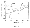
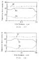
- a curve 21a of Fig. 2 shows the result obtained by measuring the Na distribution in the thickness direction of the CuInSe 2 : Na thin film having a Na content of 5 atomic% by secondary ion mass spectroscopy (SIMS).
- An axis of abscissa indicates a film thickness, wherein a film thickness of 0 represents the surface of the formed film. It is apparent that Na is uniformly distributed in the direction of the film thickness.
- Fig. 3 shows the change of the conductivity of the CuInSe 2 : Na thin film with Na content. It is apparent that the conductivity rises as the Na content is increased. If the Na content is less than 5 atomic%, the conductivity rises rectilinearly. When the Na content reaches 10 atomic%, the rising rate is decreased. The reason is that Na contained in the film functions as a dopant effectively with the Na content of 5 atomic% or less to increase a carrier concentration and that the rate at which Na contained in the film functions as the dopant is decreased with the Na content of 10 atomic%. In some cases, a large amount of dopant greatly changes the properties of a semiconductor. It is apparent that the Na content is preferably 5 atomic% or less in the present example.
- the carrier concentration of the semiconductor thin film having a chalcopyrite structure which is finally obtained can be controlled by the amount of the element added as a dopant.
- the carrier distribution becomes uniform.
- an oxide precursor in which the amount of Na is distributed in the thickness direction of the film can be formed.
- a sintered body of Cu 2 In 2 O 5 Na 2 O 2 having Na content of 10 atomic% is used as a target 3 shown in Fig. 4, and a sintered body of Cu 2 In 2 O 5 which does not contain Na is used as a target 4 shown in Fig. 4.
- These targets are simultaneously sputtered in the Ar atmosphere containing 5 vol% of O 2 at a vacuum of 8 x 10 -3 Torr.
- the reference numeral 30 designates a gas inlet, and the reference numeral 31 designates a gas outlet.
- shielding plates 5 and 6 were opened, and particles flying from the sputtered targets were deposited on a substrate 8 during rotation of a substrate holding table 7 in order to obtain a uniform composition across the film surface direction.
- the applied power of high voltage power supplies 10 and 11 of the targets By adjusting the applied power of high voltage power supplies 10 and 11 of the targets, the speed at which Cu-In-O : Na 2 O 2 and Cu-In-O are deposited can be controlled. Accordingly, the power applied to the targets is changed so that the Cu-In-O : Na 2 O 2 film in which the amount of Na is distributed in the direction of a film thickness can be deposited on the substrate.
- a curve 21b of Fig. 2 shows the result obtained by measuring the Na distribution of the CuInSe 2 : Na thin film, which is reduced by heat treating the Cu-In-O : Na 2 O 2 film under the above conditions, by secondary ion mass spectroscopy (SIMS). It is apparent that the amount of Na is increased from the film surface side to the film substrate side in the direction of a thickness.
- SIMS secondary ion mass spectroscopy
- the Na distribution of the precursor is essentially maintained in the semiconductor thin film having a chalcopyrite structure.
- the element which acts as the dopant of the precursor is distributed in the thickness direction so that the distribution of a carrier concentration described above can be formed in the direction of the thickness of the semiconductor thin film. Consequently, the efficiency of the solar cell can be enhanced.
- Na of the Ia-group element was used as the dopant in the present example. Also in the case where P of the Va-group element and Nb and Ta of the Vb-group element were used, the same results were obtained. In particular, when using Nb and Ta, the distribution of the dopant element of the precursor was maintained in the final CuInSe 2 film almost completely.
- Fig. 5 is a sectional view showing the structure of a precursor formed of an oxide thin film according to an embodiment of the present invention.
- a stainless steel substrate coated with Mo was used as a substrate 12.
- a Cu-In-Ga-O : K 2 O 2 film 13 having a K content of 2 atomic%, a Cu-In-Ga-O : K 2 O 2 film 14 having a K content of 1 atomic%, and a Cu-In-Ga-O : K 2 O 2 film 15 having a K content of 5 atomic% were sequentially deposited on the substrate 12. Deposition was performed by sputtering under the same conditions as in Example 1.
- Each film was produced by using a target in which K 2 O 2 is contained in Cu 2 In 2 O 5 in such a manner that the K content has the above ratio.
- a curve 22 shows the result obtained by measuring the K distribution in the thickness direction of the Cu(In, Ga)S 2 : K thin film by SIMS. Although slight diffusion is caused by heat treatment, the K distribution shown in Fig. 2 almost corresponded to the K distribution obtained when manufacturing the precursor.
- the present invention is effective in optionally distributing the elements as dopants in the oxide thin film with great precision.
- Fig. 6 is a sectional view showing the structure of a precursor formed of an oxide thin film according to another embodiment of the present invention.
- a glass substrate coated with a Mo film was used as a substrate 16.
- An Ia-group oxide thin film 17, i.e. Li 2 O 2 was deposited on the substrate 16.
- the Li 2 O 2 film was produced by high-frequency sputtering a Li 2 O 2 target at 1 KW in an Ar atmosphere containing about 5 vol% of O 2 at a vacuum of 8 x 10 -3 Torr.
- the Cu-In-O film was produced by the sputtering method in the Ar atmosphere containing 5 vol% of O 2 at a vacuum of 8 x 10 -3 Torr by means of a sintered body of Cu 2 In 2 O 5 as a target.
- Five kinds of films were produced, in which the thickness of the Li 2 O 2 film as a first layer is varied within 10 to 100 nm.
- the thickness of the Cu-In-O film was constant, i.e., 0.8 ⁇ m.
- the obtained oxide precursors were put in a silica tube and heat treated for 1 hr. at a temperature of 550°C in the mixed CS 2 and CO atmosphere in which H 2 gas was flowed as a carrier gas.
- CuInS 2 Li films were produced.
- the Cu-In-O film was produced by the sputtering method under the same conditions as in Example 3.
- the MgO film was produced in the Ar atmosphere containing 10 vol% of O 2 at a vacuum of 8 x 10 -3 Torr by the high frequency magnetron sputtering method in which a MgO sintered body acts as a target. MgO thus produced had a thickness of 50 nm.
- the obtained oxide precursor was put in a silica tube and heat treated for 1 hr. at a temperature of 550°C in the mixed H 2 and H 2 S atmosphere.
- the CuInS 2 film in which P and Mg are partially doped was produced.
Landscapes
- Chemical & Material Sciences (AREA)
- Chemical Kinetics & Catalysis (AREA)
- Engineering & Computer Science (AREA)
- Materials Engineering (AREA)
- Mechanical Engineering (AREA)
- Metallurgy (AREA)
- Organic Chemistry (AREA)
- Photovoltaic Devices (AREA)
- Physical Deposition Of Substances That Are Components Of Semiconductor Devices (AREA)
Applications Claiming Priority (4)
| Application Number | Priority Date | Filing Date | Title |
|---|---|---|---|
| JP11616495A JP3484259B2 (ja) | 1995-05-15 | 1995-05-15 | 半導体薄膜形成用前駆体及び半導体薄膜の製造方法 |
| JP116164/95 | 1995-05-15 | ||
| JP14199995 | 1995-06-08 | ||
| JP141999/95 | 1995-06-08 |
Publications (2)
| Publication Number | Publication Date |
|---|---|
| EP0743686A2 true EP0743686A2 (de) | 1996-11-20 |
| EP0743686A3 EP0743686A3 (de) | 1998-12-02 |
Family
ID=26454541
Family Applications (1)
| Application Number | Title | Priority Date | Filing Date |
|---|---|---|---|
| EP96107692A Withdrawn EP0743686A3 (de) | 1995-05-15 | 1996-05-14 | Vorprodukt für Halbleiterdünnschichten und Verfahren zur Herstellung von Halbleiterdünnschichten |
Country Status (2)
| Country | Link |
|---|---|
| US (1) | US5728231A (de) |
| EP (1) | EP0743686A3 (de) |
Cited By (11)
| Publication number | Priority date | Publication date | Assignee | Title |
|---|---|---|---|---|
| WO1999017889A3 (en) * | 1997-10-02 | 1999-11-11 | Chris Eberspacher | Method for forming solar cell materials from particulates |
| US6153895A (en) * | 1997-01-24 | 2000-11-28 | Asahi Kasei Kogyo Kabushiki Kaisha | p-type semiconductor, method for manufacturing the p-type semiconductor, semiconductor device, photovoltaic element, and method for manufacturing semiconductor device |
| EP0978882A3 (de) * | 1998-07-02 | 2003-08-20 | International Solar Electric Technology, Inc. | Verfahren auf Oxyd-Basis zur Herstellung von dünnen Schichten von Verbindungshalbleitern und von entsprechenden elektronischen Vorrichtungen |
| WO2013090131A3 (en) * | 2011-12-15 | 2013-09-26 | Dow Global Technologies Llc | Method of forming optoelectronic device having a stabilized metal oxide layer |
| CN105659390A (zh) * | 2013-06-05 | 2016-06-08 | 索尔伏打电流公司 | 太阳能电池结构及其制造方法 |
| US9786807B2 (en) | 2011-04-19 | 2017-10-10 | Empa | Thin-film photovoltaic device and fabrication method |
| US9837565B2 (en) | 2012-12-21 | 2017-12-05 | Flison Ag | Fabricating thin-film optoelectronic devices with added potassium |
| US10109761B2 (en) | 2014-05-23 | 2018-10-23 | Flisom Ag | Fabricating thin-film optoelectronic devices with modified surface |
| US10396218B2 (en) | 2014-09-18 | 2019-08-27 | Flisom Ag | Self-assembly pattering for fabricating thin-film devices |
| US10651324B2 (en) | 2016-02-11 | 2020-05-12 | Flisom Ag | Self-assembly patterning for fabricating thin-film devices |
| US10658532B2 (en) | 2016-02-11 | 2020-05-19 | Flisom Ag | Fabricating thin-film optoelectronic devices with added rubidium and/or cesium |
Families Citing this family (67)
| Publication number | Priority date | Publication date | Assignee | Title |
|---|---|---|---|---|
| US6323417B1 (en) | 1998-09-29 | 2001-11-27 | Lockheed Martin Corporation | Method of making I-III-VI semiconductor materials for use in photovoltaic cells |
| WO2001037324A1 (en) | 1999-11-16 | 2001-05-25 | Midwest Research Institute | A NOVEL PROCESSING APPROACH TOWARDS THE FORMATION OF THIN-FILM Cu(In,Ga)Se¿2? |
| US6815736B2 (en) | 2001-02-09 | 2004-11-09 | Midwest Research Institute | Isoelectronic co-doping |
| US6743488B2 (en) | 2001-05-09 | 2004-06-01 | Cpfilms Inc. | Transparent conductive stratiform coating of indium tin oxide |
| US7053294B2 (en) * | 2001-07-13 | 2006-05-30 | Midwest Research Institute | Thin-film solar cell fabricated on a flexible metallic substrate |
| EP1556902A4 (de) * | 2002-09-30 | 2009-07-29 | Miasole | Herstellungsvorrichtung und verfahren zur produktion von dünnfilmsolarzellen in grossem massstab |
| US20060057766A1 (en) * | 2003-07-08 | 2006-03-16 | Quanxi Jia | Method for preparation of semiconductive films |
| JP4386747B2 (ja) * | 2004-01-28 | 2009-12-16 | 三洋電機株式会社 | p型ZnO半導体膜及びその製造方法 |
| US8329501B1 (en) | 2004-02-19 | 2012-12-11 | Nanosolar, Inc. | High-throughput printing of semiconductor precursor layer from inter-metallic microflake particles |
| US20060060237A1 (en) * | 2004-09-18 | 2006-03-23 | Nanosolar, Inc. | Formation of solar cells on foil substrates |
| US7604843B1 (en) | 2005-03-16 | 2009-10-20 | Nanosolar, Inc. | Metallic dispersion |
| US8642455B2 (en) * | 2004-02-19 | 2014-02-04 | Matthew R. Robinson | High-throughput printing of semiconductor precursor layer from nanoflake particles |
| US20070163642A1 (en) * | 2004-02-19 | 2007-07-19 | Nanosolar, Inc. | High-throughput printing of semiconductor precursor layer from inter-metallic microflake articles |
| US7306823B2 (en) * | 2004-09-18 | 2007-12-11 | Nanosolar, Inc. | Coated nanoparticles and quantum dots for solution-based fabrication of photovoltaic cells |
| US20070169812A1 (en) * | 2004-02-19 | 2007-07-26 | Nanosolar, Inc. | High-throughput printing of semiconductor precursor layer from nanoflake particles |
| US20070169811A1 (en) * | 2004-02-19 | 2007-07-26 | Nanosolar, Inc. | High-throughput printing of semiconductor precursor layer by use of thermal and chemical gradients |
| US20070169813A1 (en) * | 2004-02-19 | 2007-07-26 | Nanosolar, Inc. | High-throughput printing of semiconductor precursor layer from microflake particles |
| US8372734B2 (en) * | 2004-02-19 | 2013-02-12 | Nanosolar, Inc | High-throughput printing of semiconductor precursor layer from chalcogenide nanoflake particles |
| US8309163B2 (en) * | 2004-02-19 | 2012-11-13 | Nanosolar, Inc. | High-throughput printing of semiconductor precursor layer by use of chalcogen-containing vapor and inter-metallic material |
| US20070163641A1 (en) * | 2004-02-19 | 2007-07-19 | Nanosolar, Inc. | High-throughput printing of semiconductor precursor layer from inter-metallic nanoflake particles |
| US7700464B2 (en) * | 2004-02-19 | 2010-04-20 | Nanosolar, Inc. | High-throughput printing of semiconductor precursor layer from nanoflake particles |
| US7605328B2 (en) * | 2004-02-19 | 2009-10-20 | Nanosolar, Inc. | Photovoltaic thin-film cell produced from metallic blend using high-temperature printing |
| US8048477B2 (en) * | 2004-02-19 | 2011-11-01 | Nanosolar, Inc. | Chalcogenide solar cells |
| US20070169809A1 (en) * | 2004-02-19 | 2007-07-26 | Nanosolar, Inc. | High-throughput printing of semiconductor precursor layer by use of low-melting chalcogenides |
| US7663057B2 (en) * | 2004-02-19 | 2010-02-16 | Nanosolar, Inc. | Solution-based fabrication of photovoltaic cell |
| US8846141B1 (en) * | 2004-02-19 | 2014-09-30 | Aeris Capital Sustainable Ip Ltd. | High-throughput printing of semiconductor precursor layer from microflake particles |
| US20070166453A1 (en) * | 2004-02-19 | 2007-07-19 | Nanosolar, Inc. | High-throughput printing of chalcogen layer |
| US8623448B2 (en) * | 2004-02-19 | 2014-01-07 | Nanosolar, Inc. | High-throughput printing of semiconductor precursor layer from chalcogenide microflake particles |
| US20070163639A1 (en) * | 2004-02-19 | 2007-07-19 | Nanosolar, Inc. | High-throughput printing of semiconductor precursor layer from microflake particles |
| SE0400631D0 (sv) * | 2004-03-11 | 2004-03-11 | Forskarpatent I Uppsala Ab | Thin film solar cell and manufacturing method |
| US8828479B2 (en) * | 2004-04-09 | 2014-09-09 | Honda Motor Co., Ltd. | Process for producing light absorbing layer for chalcopyrite type thin-film solar cell |
| US20050257824A1 (en) * | 2004-05-24 | 2005-11-24 | Maltby Michael G | Photovoltaic cell including capping layer |
| US20090032108A1 (en) * | 2007-03-30 | 2009-02-05 | Craig Leidholm | Formation of photovoltaic absorber layers on foil substrates |
| US8541048B1 (en) | 2004-09-18 | 2013-09-24 | Nanosolar, Inc. | Formation of photovoltaic absorber layers on foil substrates |
| CN101443929A (zh) * | 2004-11-10 | 2009-05-27 | 德斯塔尔科技公司 | 使用含碱层的过程和光电装置 |
| US20060219288A1 (en) * | 2004-11-10 | 2006-10-05 | Daystar Technologies, Inc. | Process and photovoltaic device using an akali-containing layer |
| US8927315B1 (en) | 2005-01-20 | 2015-01-06 | Aeris Capital Sustainable Ip Ltd. | High-throughput assembly of series interconnected solar cells |
| JP2009528680A (ja) * | 2006-02-23 | 2009-08-06 | デューレン、イェルーン カー.イェー. ファン | カルコゲン層の高スループット印刷および金属間化合物材料の使用 |
| EP1997150A2 (de) * | 2006-02-23 | 2008-12-03 | Van Duren, Jeroen K.J. | Mit hohem durchsatz erfolgende bestückung einer halbleiter-vorläuferschicht aus intermetallischen nanosplittern |
| CN101454486B (zh) * | 2006-04-04 | 2013-03-13 | 索罗能源公司 | 用于卷绕处理光电薄膜的组分控制 |
| US20070227633A1 (en) * | 2006-04-04 | 2007-10-04 | Basol Bulent M | Composition control for roll-to-roll processed photovoltaic films |
| US20080057203A1 (en) * | 2006-06-12 | 2008-03-06 | Robinson Matthew R | Solid group iiia particles formed via quenching |
| US7854963B2 (en) * | 2006-10-13 | 2010-12-21 | Solopower, Inc. | Method and apparatus for controlling composition profile of copper indium gallium chalcogenide layers |
| US8197703B2 (en) * | 2007-04-25 | 2012-06-12 | Solopower, Inc. | Method and apparatus for affecting surface composition of CIGS absorbers formed by two-stage process |
| WO2009046178A1 (en) * | 2007-10-02 | 2009-04-09 | University Of Delaware | I-iii-vi2 photovoltaic absorber layers |
| US8258001B2 (en) * | 2007-10-26 | 2012-09-04 | Solopower, Inc. | Method and apparatus for forming copper indium gallium chalcogenide layers |
| US8613973B2 (en) * | 2007-12-06 | 2013-12-24 | International Business Machines Corporation | Photovoltaic device with solution-processed chalcogenide absorber layer |
| US8802977B2 (en) * | 2008-05-09 | 2014-08-12 | International Business Machines Corporation | Techniques for enhancing performance of photovoltaic devices |
| ES2581378T3 (es) * | 2008-06-20 | 2016-09-05 | Volker Probst | Dispositivo de procesamiento y procedimiento para procesar productos de procesamiento apilados |
| KR20110097908A (ko) * | 2008-11-28 | 2011-08-31 | 볼커 프로브스트 | 반도체 층 또는 원소 셀레늄 및/또는 황으로 처리된 코팅 기판, 특히 평면 기판의 제조 방법 |
| US7897020B2 (en) * | 2009-04-13 | 2011-03-01 | Miasole | Method for alkali doping of thin film photovoltaic materials |
| US20110067998A1 (en) * | 2009-09-20 | 2011-03-24 | Miasole | Method of making an electrically conductive cadmium sulfide sputtering target for photovoltaic manufacturing |
| US8440498B2 (en) | 2009-10-28 | 2013-05-14 | Nanosolar, Inc. | Thin-film devices formed from solid particles |
| US20120286219A1 (en) * | 2010-01-07 | 2012-11-15 | Jx Nippon Mining & Metals Corporation | Sputtering target, semiconducting compound film, solar cell comprising semiconducting compound film, and method of producing semiconducting compound film |
| WO2011112612A1 (en) | 2010-03-08 | 2011-09-15 | Alliance For Sustainable Energy, Llc | Boron, bismuth co-doping of gallium arsenide and other compounds for photonic and heterojunction bipolar transistor devices |
| US9169548B1 (en) | 2010-10-19 | 2015-10-27 | Apollo Precision Fujian Limited | Photovoltaic cell with copper poor CIGS absorber layer and method of making thereof |
| US8048707B1 (en) | 2010-10-19 | 2011-11-01 | Miasole | Sulfur salt containing CIG targets, methods of making and methods of use thereof |
| US7935558B1 (en) | 2010-10-19 | 2011-05-03 | Miasole | Sodium salt containing CIG targets, methods of making and methods of use thereof |
| US8119513B1 (en) | 2010-11-22 | 2012-02-21 | General Electric Company | Method for making cadmium sulfide layer |
| US20120305059A1 (en) * | 2011-06-06 | 2012-12-06 | Alta Devices, Inc. | Photon recycling in an optoelectronic device |
| US20130174900A1 (en) * | 2011-07-07 | 2013-07-11 | Stion Corporation | Nanowire enhanced transparent conductive oxide for thin film photovoltaic devices |
| US8841742B2 (en) | 2011-09-27 | 2014-09-23 | Soitec | Low temperature layer transfer process using donor structure with material in recesses in transfer layer, semiconductor structures fabricated using such methods |
| US8673733B2 (en) * | 2011-09-27 | 2014-03-18 | Soitec | Methods of transferring layers of material in 3D integration processes and related structures and devices |
| US10043921B1 (en) | 2011-12-21 | 2018-08-07 | Beijing Apollo Ding Rong Solar Technology Co., Ltd. | Photovoltaic cell with high efficiency cigs absorber layer with low minority carrier lifetime and method of making thereof |
| US9082619B2 (en) | 2012-07-09 | 2015-07-14 | International Solar Electric Technology, Inc. | Methods and apparatuses for forming semiconductor films |
| JP6317877B2 (ja) | 2012-10-16 | 2018-04-25 | ローム株式会社 | 光電変換装置および光電変換装置の製造方法 |
| ES2686620T3 (es) | 2012-12-20 | 2018-10-18 | Saint-Gobain Glass France | Procedimiento para la fabricación de un semiconductor compuesto así como célula solar de capas delgadas |
Family Cites Families (5)
| Publication number | Priority date | Publication date | Assignee | Title |
|---|---|---|---|---|
| JPH0717477B2 (ja) * | 1989-03-15 | 1995-03-01 | シャープ株式会社 | 化合物半導体のエピタキシャル成長方法 |
| JPH05262504A (ja) * | 1991-09-27 | 1993-10-12 | Matsushita Electric Ind Co Ltd | 化合物半導体、その薄膜製造方法及びそれを用いた半導体装置 |
| EP0574716B1 (de) * | 1992-05-19 | 1996-08-21 | Matsushita Electric Industrial Co., Ltd. | Methode zur Herstellung einer Zusammensetzung des Typs Chalkopyrit |
| JP3064701B2 (ja) * | 1992-10-30 | 2000-07-12 | 松下電器産業株式会社 | カルコパイライト型化合物薄膜の製造方法 |
| JP3337255B2 (ja) * | 1993-02-15 | 2002-10-21 | 松下電器産業株式会社 | カルコパイライト構造半導体薄膜とその製造方法、薄膜太陽電池の製造方法、および発光装置の製造方法 |
-
1996
- 1996-05-14 EP EP96107692A patent/EP0743686A3/de not_active Withdrawn
- 1996-05-15 US US08/648,497 patent/US5728231A/en not_active Expired - Lifetime
Cited By (18)
| Publication number | Priority date | Publication date | Assignee | Title |
|---|---|---|---|---|
| US6153895A (en) * | 1997-01-24 | 2000-11-28 | Asahi Kasei Kogyo Kabushiki Kaisha | p-type semiconductor, method for manufacturing the p-type semiconductor, semiconductor device, photovoltaic element, and method for manufacturing semiconductor device |
| WO1999017889A3 (en) * | 1997-10-02 | 1999-11-11 | Chris Eberspacher | Method for forming solar cell materials from particulates |
| EP0978882A3 (de) * | 1998-07-02 | 2003-08-20 | International Solar Electric Technology, Inc. | Verfahren auf Oxyd-Basis zur Herstellung von dünnen Schichten von Verbindungshalbleitern und von entsprechenden elektronischen Vorrichtungen |
| EP1870943A3 (de) * | 1998-07-02 | 2008-03-12 | International Solar Electric Technology, Inc. | Oxidbasiertes Verfahren zur Herstellung von Verbundhalbleiterfilmen und Herstellung zugehöriger elektronischer Vorrichtungen |
| US9786807B2 (en) | 2011-04-19 | 2017-10-10 | Empa | Thin-film photovoltaic device and fabrication method |
| WO2013090131A3 (en) * | 2011-12-15 | 2013-09-26 | Dow Global Technologies Llc | Method of forming optoelectronic device having a stabilized metal oxide layer |
| US9837565B2 (en) | 2012-12-21 | 2017-12-05 | Flison Ag | Fabricating thin-film optoelectronic devices with added potassium |
| US10153387B2 (en) | 2012-12-21 | 2018-12-11 | Flisom Ag | Fabricating thin-film optoelectronic devices with added potassium |
| CN105659390B (zh) * | 2013-06-05 | 2017-11-14 | 索尔伏打电流公司 | 太阳能电池结构及其制造方法 |
| CN105659390A (zh) * | 2013-06-05 | 2016-06-08 | 索尔伏打电流公司 | 太阳能电池结构及其制造方法 |
| US10109761B2 (en) | 2014-05-23 | 2018-10-23 | Flisom Ag | Fabricating thin-film optoelectronic devices with modified surface |
| US10431709B2 (en) | 2014-05-23 | 2019-10-01 | Flisom Ag | Fabricating thin-film optoelectronic devices with modified surface |
| US10672941B2 (en) | 2014-05-23 | 2020-06-02 | Flisom Ag | Fabricating thin-film optoelectronic devices with modified surface |
| US10396218B2 (en) | 2014-09-18 | 2019-08-27 | Flisom Ag | Self-assembly pattering for fabricating thin-film devices |
| US10651324B2 (en) | 2016-02-11 | 2020-05-12 | Flisom Ag | Self-assembly patterning for fabricating thin-film devices |
| US10658532B2 (en) | 2016-02-11 | 2020-05-19 | Flisom Ag | Fabricating thin-film optoelectronic devices with added rubidium and/or cesium |
| US10971640B2 (en) | 2016-02-11 | 2021-04-06 | Flisom Ag | Self-assembly patterning for fabricating thin-film devices |
| US11257966B2 (en) | 2016-02-11 | 2022-02-22 | Flisom Ag | Fabricating thin-film optoelectronic devices with added rubidium and/or cesium |
Also Published As
| Publication number | Publication date |
|---|---|
| US5728231A (en) | 1998-03-17 |
| EP0743686A3 (de) | 1998-12-02 |
Similar Documents
| Publication | Publication Date | Title |
|---|---|---|
| US5728231A (en) | Precursor for semiconductor thin films and method for producing semiconductor thin films | |
| EP0881695B9 (de) | Verfahren zur Herstellung von dünnen Schichten aus Gruppe IB-IIIA-VIA Verbindungshalbleitern und Verfahren zur Herstellung eines photovoltäischen Bauelements | |
| US8691618B2 (en) | Metal species surface treatment of thin film photovoltaic cell and manufacturing method | |
| EP0978882B1 (de) | Verfahren auf Oxyd-Basis zur Herstellung von dünnen Schichten von Verbindungshalbleitern und von entsprechenden elektronischen Vorrichtungen | |
| US4523051A (en) | Thin films of mixed metal compounds | |
| EP0067860B1 (de) | Verfahren und vorrichtung zum herstellen von dünnschichtsolarzellen mit heteroübergängen aus i-iii-vi2-chalcopyritverbindungen und nach diesem verfahren hergestellte solarzellen | |
| US5141564A (en) | Mixed ternary heterojunction solar cell | |
| AU622617B2 (en) | Photovoltaic element with a semiconductor layer comprising non-single crystal material containing at least Zn, Se and in an amount of 1 to 40 atomic per cent | |
| US8431430B2 (en) | Method for forming a compound semi-conductor thin-film | |
| EP0306297B1 (de) | Photovoltaisches PIN-Bauelement mit einer I-Halbleiterschicht aus ZnSe oder ZnSeTe die Wasserstoff in einer Menge von 1 bis 4 Atom-% enthält | |
| EP2309548A2 (de) | Photoelektrische Umwandlungsvorrichtung, Herstellungsverfahren dafür und Solarbatterie | |
| US20080023336A1 (en) | Technique for doping compound layers used in solar cell fabrication | |
| WO2001037324A1 (en) | A NOVEL PROCESSING APPROACH TOWARDS THE FORMATION OF THIN-FILM Cu(In,Ga)Se¿2? | |
| US20120180870A1 (en) | Photoelectric conversion device, method for producing the same, and solar battery | |
| EP1517378A2 (de) | Halbleiterschicht und Herstellungsverfahren, Solarzelle mit dieser Halbleiterschicht und Herstellungsverfahren | |
| JP3484259B2 (ja) | 半導体薄膜形成用前駆体及び半導体薄膜の製造方法 | |
| JP3311873B2 (ja) | 半導体薄膜の製造方法 | |
| JP3519543B2 (ja) | 半導体薄膜形成用前駆体及び半導体薄膜の製造方法 | |
| EP2702615B1 (de) | Herstellungsverfahren für eine solarzelle | |
| JPH09213977A (ja) | 半導体薄膜の製造方法 | |
| Pisarkiewicz et al. | Fabrication of thin film polycrystalline CIS photovoltaic heterostructure | |
| Basol et al. | Preparation of Cd (Zn) Te and CuInSe2 films and devices by a two-stage process | |
| US8236597B1 (en) | Bulk metal species treatment of thin film photovoltaic cell and manufacturing method | |
| WO2025012117A1 (en) | Thin film solar cell and corresponding production method | |
| Waters | Physical vapor deposition of novel thin-film solar absorbers |
Legal Events
| Date | Code | Title | Description |
|---|---|---|---|
| PUAI | Public reference made under article 153(3) epc to a published international application that has entered the european phase |
Free format text: ORIGINAL CODE: 0009012 |
|
| AK | Designated contracting states |
Kind code of ref document: A2 Designated state(s): DE FR GB |
|
| PUAL | Search report despatched |
Free format text: ORIGINAL CODE: 0009013 |
|
| AK | Designated contracting states |
Kind code of ref document: A3 Designated state(s): DE FR GB |
|
| 17P | Request for examination filed |
Effective date: 19990304 |
|
| 17Q | First examination report despatched |
Effective date: 20000211 |
|
| STAA | Information on the status of an ep patent application or granted ep patent |
Free format text: STATUS: THE APPLICATION IS DEEMED TO BE WITHDRAWN |
|
| 18D | Application deemed to be withdrawn |
Effective date: 20010619 |