EP0744766A2 - Verfahren zur Oberflächenplanarisierung mit einem zweistufigen mechanisch-chemischen Poliervorgang - Google Patents
Verfahren zur Oberflächenplanarisierung mit einem zweistufigen mechanisch-chemischen Poliervorgang Download PDFInfo
- Publication number
- EP0744766A2 EP0744766A2 EP96480032A EP96480032A EP0744766A2 EP 0744766 A2 EP0744766 A2 EP 0744766A2 EP 96480032 A EP96480032 A EP 96480032A EP 96480032 A EP96480032 A EP 96480032A EP 0744766 A2 EP0744766 A2 EP 0744766A2
- Authority
- EP
- European Patent Office
- Prior art keywords
- polish stop
- dielectric coating
- polishing
- slurry
- dielectric
- Prior art date
- Legal status (The legal status is an assumption and is not a legal conclusion. Google has not performed a legal analysis and makes no representation as to the accuracy of the status listed.)
- Withdrawn
Links
Images
Classifications
-
- H—ELECTRICITY
- H10—SEMICONDUCTOR DEVICES; ELECTRIC SOLID-STATE DEVICES NOT OTHERWISE PROVIDED FOR
- H10P—GENERIC PROCESSES OR APPARATUS FOR THE MANUFACTURE OR TREATMENT OF DEVICES COVERED BY CLASS H10
- H10P95/00—Generic processes or apparatus for manufacture or treatments not covered by the other groups of this subclass
- H10P95/06—Planarisation of inorganic insulating materials
- H10P95/062—Planarisation of inorganic insulating materials involving a dielectric removal step
Definitions
- the present invention generally relates to the manufacture of semiconductor devices and, more particularly, to an improved planarization technique for integrated circuit wafers which produces improved planarity in the wafers in a shorter polish time.
- CMP chemical mechanical polishing
- planarization remains a critical issue.
- Combinations of reactive ion etching (RIE) with CMP have also been tried but still do not achieve the desired level of planarization.
- RIE reactive ion etching
- the combination of RIE and CMP is expensive and complex, requiring many steps and a mask. What is needed is a simpler, less expensive planarization process, preferably not requiring a mask and provides better control of the planarization process.
- the underlying layer is characterized as having elevated areas and recessed areas.
- the wafer is first prepared by applying a first polish stop on the elevated areas, then depositing a layer of dielectric over at least the recessed areas, and finally depositing a second polish stop over the resulting dielectric coating.
- the first step in the two-step CMP is polishing the second polish stop using a slurry that attacks the second polish stop until the second polish stop is substantially removed.
- the second step is polishing the dielectric coating that remains using a second slurry that attacks the dielectric at a faster rate than it attacks either the second or first polish stop until the first polish stop is exposed. In this process, the second polish stop protects the recessed areas.
- Another object of this invention is to provide a process whereby there is no first polish stop material.
- the dielectric material is deposited directly over the topographical structures with no polish stop material protecting them.
- a polish stop material is then deposited over at least the recessed areas. The objective of this polish is to planarize the dielectric but not to expose the underlying structures. Therefore, a stated amount of dielectric remains over the once elevated areas.
- This example starts with a silicon wafer which has been patterned with trenches, thus having elevated and recessed areas.
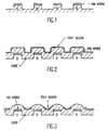
- a film of silicon nitride is formed on the elevated surface areas, to provide the structure shown in the cross-section of Figure 1. This is referred to as the pad nitride.
- this first polish stop is not required.
- a thick film of material such as oxide, is deposited to a sufficient thickness to cover the recessed areas.
- a blanket layer of polysilicon, or other appropriate material is deposited over the entire wafer to produce the structure shown in the cross-section of Figure 2.
- the first CMP step is performed using a polysilicon slurry that is highly selective to oxide. Alternatively, a slurry having either similar of reverse polish rates for oxide and polysilicon may be used.
- the end point of the first CMP step can be determined by time, visible inspection, and/or step height measurement. The goal of this first step is to remove the polysilicon from the elevated areas and leave polysilicon in the recessed areas as shown in Figure 3.
- the process continues with the second CMP step using a ceria slurry, or any slurry with sufficient selectivity between polysilicon and oxide. Since the polishing rate of oxide in ceria is much faster than that for the polysilicon, the recessed areas still covered with polysilicon are protected during the polish. In this manner, planarization can be achieved.
- End point detection can be monitored by time and/or measurement of the pad nitride thickness.
- Another approach to end point detection involves changes in friction that occur during polishing of different materials, in this case, oxide to nitride. This can be done by monitoring changes in the motor currents for the platter and carrier.
- Yet another approach for end point detection is monitoring and detecting frequency changes.
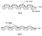
- Figure 4 is a cross-sectional view of a gate contact (GC), showing the elevated areas as the gate structure.
- GC gate contact
- a colloidal silica slurry is used in the first CMP step to produce the structure shown in Figure 5.
- This is followed by the second CMP step with a ceria, or other high selectivity, slurry. Therefore, the technique according to the invention is adaptable for both types of polish; one which incorporates two polish stops (over elevated and recessed areas) and the other which requires only one polish stop (over recessed areas only).
Landscapes
- Mechanical Treatment Of Semiconductor (AREA)
- Internal Circuitry In Semiconductor Integrated Circuit Devices (AREA)
- Crystals, And After-Treatments Of Crystals (AREA)
- Element Separation (AREA)
Applications Claiming Priority (2)
| Application Number | Priority Date | Filing Date | Title |
|---|---|---|---|
| US08/430,972 US6069081A (en) | 1995-04-28 | 1995-04-28 | Two-step chemical mechanical polish surface planarization technique |
| US430972 | 1995-04-28 |
Publications (2)
| Publication Number | Publication Date |
|---|---|
| EP0744766A2 true EP0744766A2 (de) | 1996-11-27 |
| EP0744766A3 EP0744766A3 (de) | 1996-12-27 |
Family
ID=23709888
Family Applications (1)
| Application Number | Title | Priority Date | Filing Date |
|---|---|---|---|
| EP96480032A Withdrawn EP0744766A3 (de) | 1995-04-28 | 1996-03-19 | Verfahren zur Oberflächenplanarisierung mit einem zweistufigen mechanisch-chemischen Poliervorgang |
Country Status (5)
| Country | Link |
|---|---|
| US (1) | US6069081A (de) |
| EP (1) | EP0744766A3 (de) |
| JP (1) | JP3213235B2 (de) |
| KR (1) | KR960037216A (de) |
| TW (1) | TW293145B (de) |
Cited By (6)
| Publication number | Priority date | Publication date | Assignee | Title |
|---|---|---|---|---|
| EP0813239A1 (de) * | 1996-02-21 | 1997-12-17 | Texas Instruments Incorporated | Verbesserungen bezüglich Halbleitervorrichtungen |
| EP0848416A1 (de) * | 1996-12-12 | 1998-06-17 | Texas Instruments Incorporated | Ein Ätzprozess |
| EP0916452A3 (de) * | 1997-11-12 | 2001-01-31 | LAM Research Corporation | Verfahren und Vorrichtung zum Polieren von Halbleiterscheiben |
| EP1353369A3 (de) * | 2002-03-29 | 2004-05-06 | Sharp Kabushiki Kaisha | Verfahren zur Herstellung eines Halbleiterbauelements |
| EP1608008A3 (de) * | 2004-06-18 | 2008-02-20 | Sharp Kabushiki Kaisha | Herstellungsverfahren einer Halbleitervorrichtung |
| CN111430231A (zh) * | 2020-05-21 | 2020-07-17 | 中国科学院微电子研究所 | 一种平坦化方法及半导体器件 |
Families Citing this family (15)
| Publication number | Priority date | Publication date | Assignee | Title |
|---|---|---|---|---|
| US6787471B2 (en) * | 1998-08-26 | 2004-09-07 | Renesas Technology Corp. | Method of manufacturing a semiconductor device |
| TW417236B (en) * | 1998-09-01 | 2001-01-01 | Mosel Vitelic Inc | A global planarization process |
| KR100560291B1 (ko) * | 1998-12-30 | 2006-06-19 | 주식회사 하이닉스반도체 | 반도체 소자의 콘택 플러그 형성 방법 |
| US6203404B1 (en) * | 1999-06-03 | 2001-03-20 | Micron Technology, Inc. | Chemical mechanical polishing methods |
| US6391792B1 (en) * | 2000-05-18 | 2002-05-21 | Taiwan Semiconductor Manufacturing Co., Ltd | Multi-step chemical mechanical polish (CMP) planarizing method for forming patterned planarized aperture fill layer |
| US6593240B1 (en) | 2000-06-28 | 2003-07-15 | Infineon Technologies, North America Corp | Two step chemical mechanical polishing process |
| KR100421037B1 (ko) * | 2001-03-14 | 2004-03-03 | 삼성전자주식회사 | 반도체소자의 제조방법 |
| US6485355B1 (en) | 2001-06-22 | 2002-11-26 | International Business Machines Corporation | Method to increase removal rate of oxide using fixed-abrasive |
| US6723655B2 (en) | 2001-06-29 | 2004-04-20 | Hynix Semiconductor Inc. | Methods for fabricating a semiconductor device |
| US6638866B1 (en) * | 2001-10-18 | 2003-10-28 | Taiwan Semiconductor Manufacturing Company | Chemical-mechanical polishing (CMP) process for shallow trench isolation |
| US6999668B2 (en) * | 2002-01-09 | 2006-02-14 | Matsushita Electric Industrial Co., Ltd. | Method for manufacturing optical waveguide device, optical waveguide device, and coherent light source and optical apparatus using the optical waveguide device |
| KR100532427B1 (ko) * | 2003-03-27 | 2005-11-30 | 삼성전자주식회사 | 강유전체 메모리 소자의 제조 방법 |
| CN100559553C (zh) * | 2004-03-17 | 2009-11-11 | 中芯国际集成电路制造(上海)有限公司 | 集成电路器件的化学机械抛光的终点检测方法 |
| US7125321B2 (en) * | 2004-12-17 | 2006-10-24 | Intel Corporation | Multi-platen multi-slurry chemical mechanical polishing process |
| DE102005017372A1 (de) * | 2005-04-14 | 2006-10-19 | Degussa Ag | Wässrige Ceroxiddispersion |
Family Cites Families (16)
| Publication number | Priority date | Publication date | Assignee | Title |
|---|---|---|---|---|
| US4671851A (en) * | 1985-10-28 | 1987-06-09 | International Business Machines Corporation | Method for removing protuberances at the surface of a semiconductor wafer using a chem-mech polishing technique |
| US4735679A (en) * | 1987-03-30 | 1988-04-05 | International Business Machines Corporation | Method of improving silicon-on-insulator uniformity |
| JP2541214B2 (ja) * | 1987-04-02 | 1996-10-09 | ソニー株式会社 | 半導体装置の製造方法 |
| US5514616A (en) * | 1991-08-26 | 1996-05-07 | Lsi Logic Corporation | Depositing and densifying glass to planarize layers in semi-conductor devices based on CMOS structures |
| US5244534A (en) * | 1992-01-24 | 1993-09-14 | Micron Technology, Inc. | Two-step chemical mechanical polishing process for producing flush and protruding tungsten plugs |
| US5334281A (en) * | 1992-04-30 | 1994-08-02 | International Business Machines Corporation | Method of forming thin silicon mesas having uniform thickness |
| US5445996A (en) * | 1992-05-26 | 1995-08-29 | Kabushiki Kaisha Toshiba | Method for planarizing a semiconductor device having a amorphous layer |
| JP2914860B2 (ja) * | 1992-10-20 | 1999-07-05 | 株式会社東芝 | 半導体装置とその製造方法および研磨方法ならびに研磨装置および研磨装置の研磨面の再生方法 |
| JPH07111962B2 (ja) * | 1992-11-27 | 1995-11-29 | 日本電気株式会社 | 選択平坦化ポリッシング方法 |
| US5356513A (en) * | 1993-04-22 | 1994-10-18 | International Business Machines Corporation | Polishstop planarization method and structure |
| US5362669A (en) * | 1993-06-24 | 1994-11-08 | Northern Telecom Limited | Method of making integrated circuits |
| US5395801A (en) * | 1993-09-29 | 1995-03-07 | Micron Semiconductor, Inc. | Chemical-mechanical polishing processes of planarizing insulating layers |
| US5340370A (en) * | 1993-11-03 | 1994-08-23 | Intel Corporation | Slurries for chemical mechanical polishing |
| US5385866A (en) * | 1994-06-22 | 1995-01-31 | International Business Machines Corporation | Polish planarizing using oxidized boron nitride as a polish stop |
| US5459096A (en) * | 1994-07-05 | 1995-10-17 | Motorola Inc. | Process for fabricating a semiconductor device using dual planarization layers |
| US5483568A (en) * | 1994-11-03 | 1996-01-09 | Kabushiki Kaisha Toshiba | Pad condition and polishing rate monitor using fluorescence |
-
1995
- 1995-04-28 US US08/430,972 patent/US6069081A/en not_active Expired - Lifetime
-
1996
- 1996-03-19 EP EP96480032A patent/EP0744766A3/de not_active Withdrawn
- 1996-03-21 TW TW085103521A patent/TW293145B/zh active
- 1996-04-24 JP JP10218396A patent/JP3213235B2/ja not_active Expired - Fee Related
- 1996-04-25 KR KR1019960012816A patent/KR960037216A/ko not_active Abandoned
Cited By (10)
| Publication number | Priority date | Publication date | Assignee | Title |
|---|---|---|---|---|
| EP0813239A1 (de) * | 1996-02-21 | 1997-12-17 | Texas Instruments Incorporated | Verbesserungen bezüglich Halbleitervorrichtungen |
| US5909628A (en) * | 1996-02-21 | 1999-06-01 | Texas Instruments Incorporated | Reducing non-uniformity in a refill layer thickness for a semiconductor device |
| EP0848416A1 (de) * | 1996-12-12 | 1998-06-17 | Texas Instruments Incorporated | Ein Ätzprozess |
| EP0916452A3 (de) * | 1997-11-12 | 2001-01-31 | LAM Research Corporation | Verfahren und Vorrichtung zum Polieren von Halbleiterscheiben |
| US6336845B1 (en) | 1997-11-12 | 2002-01-08 | Lam Research Corporation | Method and apparatus for polishing semiconductor wafers |
| US6416385B2 (en) | 1997-11-12 | 2002-07-09 | Lam Research Corporation | Method and apparatus for polishing semiconductor wafers |
| US6517418B2 (en) | 1997-11-12 | 2003-02-11 | Lam Research Corporation | Method of transporting a semiconductor wafer in a wafer polishing system |
| EP1353369A3 (de) * | 2002-03-29 | 2004-05-06 | Sharp Kabushiki Kaisha | Verfahren zur Herstellung eines Halbleiterbauelements |
| EP1608008A3 (de) * | 2004-06-18 | 2008-02-20 | Sharp Kabushiki Kaisha | Herstellungsverfahren einer Halbleitervorrichtung |
| CN111430231A (zh) * | 2020-05-21 | 2020-07-17 | 中国科学院微电子研究所 | 一种平坦化方法及半导体器件 |
Also Published As
| Publication number | Publication date |
|---|---|
| JP3213235B2 (ja) | 2001-10-02 |
| KR960037216A (ko) | 1996-11-19 |
| JPH0997774A (ja) | 1997-04-08 |
| US6069081A (en) | 2000-05-30 |
| EP0744766A3 (de) | 1996-12-27 |
| TW293145B (de) | 1996-12-11 |
Similar Documents
| Publication | Publication Date | Title |
|---|---|---|
| US6069081A (en) | Two-step chemical mechanical polish surface planarization technique | |
| US5272117A (en) | Method for planarizing a layer of material | |
| US5923993A (en) | Method for fabricating dishing free shallow isolation trenches | |
| US5872043A (en) | Method of planarizing wafers with shallow trench isolation | |
| EP0637071B1 (de) | Verfahren zum Ebnen eines Isolationsgrabens für IC unter Verwendung eines Fillers aus Polysilizium | |
| US5459096A (en) | Process for fabricating a semiconductor device using dual planarization layers | |
| US5321304A (en) | Detecting the endpoint of chem-mech polishing, and resulting semiconductor device | |
| US5302233A (en) | Method for shaping features of a semiconductor structure using chemical mechanical planarization (CMP) | |
| US6017803A (en) | Method to prevent dishing in chemical mechanical polishing | |
| EP0603097A2 (de) | Als Polierstoppschicht für die Herstellung vom Substraten von SOI-Typ verwendetes Nitrit | |
| JP2001015460A (ja) | 半導体装置の製造方法 | |
| WO2001013425A1 (en) | Manufacture of an integrated circuit isolation structure | |
| US6541349B2 (en) | Shallow trench isolation using non-conformal dielectric and planarizatrion | |
| US20020039874A1 (en) | Temperature endpointing of chemical mechanical polishing | |
| US6171929B1 (en) | Shallow trench isolator via non-critical chemical mechanical polishing | |
| WO2000002235A1 (en) | Method of planarizing integrated circuits | |
| US6165869A (en) | Method to avoid dishing in forming trenches for shallow trench isolation | |
| US5928961A (en) | Dishing inhibited shallow trench isolation | |
| US6242352B1 (en) | Method of preventing micro-scratches on the surface of a semiconductor wafer when performing a CMP process | |
| US6265325B1 (en) | Method for fabricating dual gate dielectric layers | |
| JP3161425B2 (ja) | Stiの形成方法 | |
| US6190999B1 (en) | Method for fabricating a shallow trench isolation structure | |
| EP0791954A2 (de) | Verfahren zum Einebenen von Halbleiterschichten | |
| US6387808B1 (en) | Method of correcting topographical effects on a micro-electronic substrate | |
| HK1007259A (en) | Two-step chemical mechanical polish surface planarization technique |
Legal Events
| Date | Code | Title | Description |
|---|---|---|---|
| PUAI | Public reference made under article 153(3) epc to a published international application that has entered the european phase |
Free format text: ORIGINAL CODE: 0009012 |
|
| PUAL | Search report despatched |
Free format text: ORIGINAL CODE: 0009013 |
|
| AK | Designated contracting states |
Kind code of ref document: A2 Designated state(s): AT DE FR GB IE IT NL |
|
| AK | Designated contracting states |
Kind code of ref document: A3 Designated state(s): AT DE FR GB IE IT NL |
|
| 17P | Request for examination filed |
Effective date: 19970213 |
|
| 17Q | First examination report despatched |
Effective date: 19971002 |
|
| STAA | Information on the status of an ep patent application or granted ep patent |
Free format text: STATUS: THE APPLICATION HAS BEEN WITHDRAWN |
|
| 18W | Application withdrawn |
Withdrawal date: 20000320 |
|
| REG | Reference to a national code |
Ref country code: HK Ref legal event code: WD Ref document number: 1007259 Country of ref document: HK |