EP0603097A2 - Als Polierstoppschicht für die Herstellung vom Substraten von SOI-Typ verwendetes Nitrit - Google Patents
Als Polierstoppschicht für die Herstellung vom Substraten von SOI-Typ verwendetes Nitrit Download PDFInfo
- Publication number
- EP0603097A2 EP0603097A2 EP93480176A EP93480176A EP0603097A2 EP 0603097 A2 EP0603097 A2 EP 0603097A2 EP 93480176 A EP93480176 A EP 93480176A EP 93480176 A EP93480176 A EP 93480176A EP 0603097 A2 EP0603097 A2 EP 0603097A2
- Authority
- EP
- European Patent Office
- Prior art keywords
- layer
- polish stop
- apertures
- silicon mesas
- polish
- Prior art date
- Legal status (The legal status is an assumption and is not a legal conclusion. Google has not performed a legal analysis and makes no representation as to the accuracy of the status listed.)
- Withdrawn
Links
Images
Classifications
-
- H—ELECTRICITY
- H10—SEMICONDUCTOR DEVICES; ELECTRIC SOLID-STATE DEVICES NOT OTHERWISE PROVIDED FOR
- H10P—GENERIC PROCESSES OR APPARATUS FOR THE MANUFACTURE OR TREATMENT OF DEVICES COVERED BY CLASS H10
- H10P52/00—Grinding, lapping or polishing of wafers, substrates or parts of devices
- H10P52/40—Chemomechanical polishing [CMP]
- H10P52/403—Chemomechanical polishing [CMP] of conductive or resistive materials
-
- H—ELECTRICITY
- H10—SEMICONDUCTOR DEVICES; ELECTRIC SOLID-STATE DEVICES NOT OTHERWISE PROVIDED FOR
- H10P—GENERIC PROCESSES OR APPARATUS FOR THE MANUFACTURE OR TREATMENT OF DEVICES COVERED BY CLASS H10
- H10P90/00—Preparation of wafers not covered by a single main group of this subclass, e.g. wafer reinforcement
- H10P90/19—Preparing inhomogeneous wafers
- H10P90/1904—Preparing vertically inhomogeneous wafers
- H10P90/1906—Preparing SOI wafers
- H10P90/1914—Preparing SOI wafers using bonding
-
- H—ELECTRICITY
- H10—SEMICONDUCTOR DEVICES; ELECTRIC SOLID-STATE DEVICES NOT OTHERWISE PROVIDED FOR
- H10W—GENERIC PACKAGES, INTERCONNECTIONS, CONNECTORS OR OTHER CONSTRUCTIONAL DETAILS OF DEVICES COVERED BY CLASS H10
- H10W10/00—Isolation regions in semiconductor bodies between components of integrated devices
- H10W10/01—Manufacture or treatment
- H10W10/061—Manufacture or treatment using SOI processes together with lateral isolation, e.g. combinations of SOI and shallow trench isolations
-
- H—ELECTRICITY
- H10—SEMICONDUCTOR DEVICES; ELECTRIC SOLID-STATE DEVICES NOT OTHERWISE PROVIDED FOR
- H10W—GENERIC PACKAGES, INTERCONNECTIONS, CONNECTORS OR OTHER CONSTRUCTIONAL DETAILS OF DEVICES COVERED BY CLASS H10
- H10W10/00—Isolation regions in semiconductor bodies between components of integrated devices
- H10W10/10—Isolation regions comprising dielectric materials
- H10W10/181—Semiconductor-on-insulator [SOI] isolation regions, e.g. buried oxide regions of SOI wafers
-
- H—ELECTRICITY
- H10—SEMICONDUCTOR DEVICES; ELECTRIC SOLID-STATE DEVICES NOT OTHERWISE PROVIDED FOR
- H10P—GENERIC PROCESSES OR APPARATUS FOR THE MANUFACTURE OR TREATMENT OF DEVICES COVERED BY CLASS H10
- H10P90/00—Preparation of wafers not covered by a single main group of this subclass, e.g. wafer reinforcement
- H10P90/19—Preparing inhomogeneous wafers
- H10P90/1904—Preparing vertically inhomogeneous wafers
- H10P90/1906—Preparing SOI wafers
- H10P90/1908—Preparing SOI wafers using silicon implanted buried insulating layers, e.g. oxide layers [SIMOX]
-
- H—ELECTRICITY
- H10—SEMICONDUCTOR DEVICES; ELECTRIC SOLID-STATE DEVICES NOT OTHERWISE PROVIDED FOR
- H10W—GENERIC PACKAGES, INTERCONNECTIONS, CONNECTORS OR OTHER CONSTRUCTIONAL DETAILS OF DEVICES COVERED BY CLASS H10
- H10W10/00—Isolation regions in semiconductor bodies between components of integrated devices
- H10W10/01—Manufacture or treatment
- H10W10/011—Manufacture or treatment of isolation regions comprising dielectric materials
- H10W10/014—Manufacture or treatment of isolation regions comprising dielectric materials using trench refilling with dielectric materials, e.g. shallow trench isolations
-
- H—ELECTRICITY
- H10—SEMICONDUCTOR DEVICES; ELECTRIC SOLID-STATE DEVICES NOT OTHERWISE PROVIDED FOR
- H10W—GENERIC PACKAGES, INTERCONNECTIONS, CONNECTORS OR OTHER CONSTRUCTIONAL DETAILS OF DEVICES COVERED BY CLASS H10
- H10W10/00—Isolation regions in semiconductor bodies between components of integrated devices
- H10W10/10—Isolation regions comprising dielectric materials
- H10W10/17—Isolation regions comprising dielectric materials formed using trench refilling with dielectric materials, e.g. shallow trench isolations
-
- Y—GENERAL TAGGING OF NEW TECHNOLOGICAL DEVELOPMENTS; GENERAL TAGGING OF CROSS-SECTIONAL TECHNOLOGIES SPANNING OVER SEVERAL SECTIONS OF THE IPC; TECHNICAL SUBJECTS COVERED BY FORMER USPC CROSS-REFERENCE ART COLLECTIONS [XRACs] AND DIGESTS
- Y10—TECHNICAL SUBJECTS COVERED BY FORMER USPC
- Y10S—TECHNICAL SUBJECTS COVERED BY FORMER USPC CROSS-REFERENCE ART COLLECTIONS [XRACs] AND DIGESTS
- Y10S148/00—Metal treatment
- Y10S148/168—V-Grooves
-
- Y—GENERAL TAGGING OF NEW TECHNOLOGICAL DEVELOPMENTS; GENERAL TAGGING OF CROSS-SECTIONAL TECHNOLOGIES SPANNING OVER SEVERAL SECTIONS OF THE IPC; TECHNICAL SUBJECTS COVERED BY FORMER USPC CROSS-REFERENCE ART COLLECTIONS [XRACs] AND DIGESTS
- Y10—TECHNICAL SUBJECTS COVERED BY FORMER USPC
- Y10S—TECHNICAL SUBJECTS COVERED BY FORMER USPC CROSS-REFERENCE ART COLLECTIONS [XRACs] AND DIGESTS
- Y10S438/00—Semiconductor device manufacturing: process
- Y10S438/977—Thinning or removal of substrate
Definitions
- the field of the invention is that of forming SOI integrated circuits using bonded oxide wafers, in which the thin silicon device layer is polished down to a smaller thickness.
- Thin device layers made by implanting oxygen and forming the buried oxide insulating layer in situ are commercially available, but the top surface of the buried insulator normally has crystal defects that produce leaky devices.
- U S-A- 4 735 679 illustrates a technique for providing thin uniform layers of top silicon, called device silicon, above an underlying oxide insulator to form SOI integrated circuits.
- This patent illustrates a technique in which a polish stop of refractory metal, defined by a lift off technique, is used to define the uniformity of the silicon device layer.
- U S-A- 4 824 755 illustrates a process that uses a concentration dependent oxidation process which leads to a RIE step that is not well controlled and therefore will have manufacturing difficulty. Further, the use of side crystallization of the polysilicon means that defects in the crystal structure will be located in the transistor area.
- the invention relates to a process for forming thin (100nm or less) silicon on insulator (SOI) for submicron CMOS technology.
- SOI silicon on insulator
- the device layer oriented in the ⁇ 100> direction is etched down to the buried oxide using KOH as etchant through an aperture in a temporary nitride layer, forming a polish stop aperture with slanting sidewalls with the (111) planes of the device layer serving as a lateral etch stop.
- a polish stop nitride layer of controlled thickness is deposited on the bottom of the apertures and on the sides, after which the nitride outside the bottom of the aperture is removed to leave a set of polish stops on the bottom of the aperture that will define the thickness of mesas in the device layer.
- the silicon device layer is then polished down to the height of these polish stops and transistors are formed in the silicon mesas.
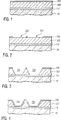
- FIGS 1 through 8 illustrate in cross-section an area of an integrated circuit wafer being formed according to the invention.
- a silicon substrate 10 having a conventional thickness at the top of which a bonding oxide layer 110 forms the bond between wafer 10 and the thinned down device layer 200, which originally was a second silicon wafer of the same thickness as wafer 10 and having the ⁇ 100> orientation.
- Device layer 200 has been thinned down from its commercial thickness of 2 ⁇ m to a thickness of less than 1 ⁇ m by repeated steps of oxidation, as is known in the art.
- the top layer 300 is a temporary protective layer of nitride having a nominal thickness of 200nm.
- nitride layer 300 has formed therein two apertures 310 that will be the positions of the polish stops.
- the area between apertures 310 in device layer 200 are thick silicon mesas that will be polished down to form final silicon mesas for holding the transistors, illustratively field effect transistors.
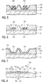
- a wet etch of KOH potassium hydroxide
- KOH potassium hydroxide
- oxide layer 110 serving as an etch stop for the bottom of apertures 250.
- the slanting sidewalls of layer 200 form a very good etch stop, as silicon in the ⁇ 100> orientation has very good etch resistance along the (111) crystal planes.
- the lateral dimensions of apertures 250 are very well controlled, since the etch extends down until oxide layer 110 is reached, after which the etching stops on the (111) planes that extend up from the oxide.
- the nominal width of apertures 310 is set by the fact that the angle of the (111) plane with respect to the (001) plane is 54.7°.
- Fig. 3 shows a slight overhang for layer 300 because the (111) planes are not perfect etch stops. It has been observed that the amount of overhang is quite small, so that the apertures are easily controllable even with a conventional amount of overetch and the location of the final silicon mesas is well defined by the standards of submicron technology. Those skilled in the art will readily be able to calculate the required width of apertures 310 based on the desired width at the bottom of the aperture and the thickness of layer 200.
- the size of the final silicon mesas will be determined by the circuit layout and may range from one mesa per transistor to large mesas containing many transistors.
- Polish stop size and density will be determined by the mesa size and the polishing process.
- the density of polish stops will be set to avoid "dishing" of the mesas. Since the mesas are extremely thin, the density of polish stops will be high. Polish stops may extend to surround mesas or may be placed in the interior of large mesas.
- Fig. 3 there is a minimum size mesa for a given thickness of layer 200, set by the requirement that there be at least a predetermined minimum amount of nitride remaining above a mesa when the apertures are defined. For example, if there were no nitride left above the central mesa in Fig. 3, the two apertures 250 would merge into one big aperture. After the etch, the remainder of layer 300 is stripped in hot phosphoric acid.
- the wet etch has removed a substantial amount of device layer 200, in contrast to a conventional polish stop process, in which the amount of material removed during the formation of the polish stop is small.
- the material removal process in this method is carried out in two separate steps - the first being the aperture definition process and the second being the chemical-mechanical polishing process. When the density of polish stops is high, more material may be removed in the aperture definition process than in the polishing process.
- a layer of nitride 350 has been deposited to a controlled thickness of between 50 and 100nm, depending on the desired SOI device thickness, at the bottom of the aperture.
- the thickness on the sides of the aperture or the general horizontal surface does not matter.
- the parameters of this low pressure chemical vapor deposition (LPCVD) process are set as is known in the art in order to deposit an isotropic and uniform nitride layer.
- the preferred deposition temperature is about 780°C, but reasonable uniformity is produced above 600°C.
- photoresist 360 has been deposited and patterned in a conventional lithographic step to protect the nitride polish stop layer 350 in the bottom of apertures 250.
- a reactive ion etch (RIE) step using CHF3 + CF4 + Ar as an etching gas (and using end point detection on silicon) has removed nitride layer 350 from the unprotected areas and along the angled silicon surfaces and also reduced the thickness of the photoresist layer 360 to a residual amount denoted with the numeral 365.
- Photoresist 365 is stripped away, leaving a polish stop stud 355 in each aperture.
- a layer of polycrystalline silicon (poly) 370 is deposited over the wafer above 10nm of oxide 205 that has been grown on the exposed silicon, as shown in Fig. 7.
- the thickness of poly layer 370 is not critical, being nominally greater in thickness than nitride layer 350.
- Poly layer 370 is an optional process step, its purpose being to provide mechanical support to the layer 200 during the polishing step. It has been found that polishing with an empty aperture causes damage to the exposed edges of the silicon and that this damage may propagate down to the silicon that is intended to hold the devices. Such damage is eliminated by the support of layer 370 which preferably fills apertures 250.
- Poly layer 370 has the added virtue that it fills in the small empty spaces between nitride polish stops 355 and the remaining portion of device layer 200, indicated by the brackets labelled 357. This filling produces greater planarity in the final set of silicon mesas.
- a conventional chemical-mechanical polishing process has been performed using nitride buttons 355 as polish stops.
- the result is that device layer 200 has been thinned, leaving a set of silicon mesas 210 having the thickness of polish stops 355, and the uniformity of these same polish stops, nominally ⁇ 5nm.
- Nitride polish stops 355 may be removed if desired to provide additional isolation between the silicon mesas of layer 200.
- a field effect transistor 390 having gate 392, drain 394 and source 396 is shown.
- transistor 390 is a depletion type transistor having a gate width of 0.25 ⁇ m, a value of five times the thickness of mesa 210, illustratively 50nm.
- An advantage of the present invention is that the wet etching process does not sacrifice silicon area because of lateral etching. Ordinarily, wet etching is not considered for high definition processes such as that to be performed in the silicon mesas because of the lack of a lateral etch stop.
- any lateral overetch that may result because the (111) planes are not perfect etch stops is harmless because that material would have had to be polished away anyway.
- the alignment of the initial apertures 310 is not critical, and there is only one critical alignment in this process.
- layer 300 could be replaced with photoresist or oxide.
- the polish stop layer could be oxide, with appropriate changes in the etching gas.
Landscapes
- Element Separation (AREA)
- Mechanical Treatment Of Semiconductor (AREA)
Applications Claiming Priority (2)
| Application Number | Priority Date | Filing Date | Title |
|---|---|---|---|
| US991222 | 1992-12-16 | ||
| US07/991,222 US5262346A (en) | 1992-12-16 | 1992-12-16 | Nitride polish stop for forming SOI wafers |
Publications (1)
| Publication Number | Publication Date |
|---|---|
| EP0603097A2 true EP0603097A2 (de) | 1994-06-22 |
Family
ID=25536995
Family Applications (1)
| Application Number | Title | Priority Date | Filing Date |
|---|---|---|---|
| EP93480176A Withdrawn EP0603097A2 (de) | 1992-12-16 | 1993-11-04 | Als Polierstoppschicht für die Herstellung vom Substraten von SOI-Typ verwendetes Nitrit |
Country Status (3)
| Country | Link |
|---|---|
| US (1) | US5262346A (de) |
| EP (1) | EP0603097A2 (de) |
| JP (1) | JPH06318687A (de) |
Cited By (1)
| Publication number | Priority date | Publication date | Assignee | Title |
|---|---|---|---|---|
| DE10149195A1 (de) * | 2001-10-05 | 2003-04-24 | Infineon Technologies Ag | Verfahren zum Herstellen einer integrierten Schaltung mit einer auf einem Dielektrikum angeordneten leitfähigen Struktur |
Families Citing this family (24)
| Publication number | Priority date | Publication date | Assignee | Title |
|---|---|---|---|---|
| US5405454A (en) * | 1992-03-19 | 1995-04-11 | Matsushita Electric Industrial Co., Ltd. | Electrically insulated silicon structure and producing method therefor |
| JP3060714B2 (ja) * | 1992-04-15 | 2000-07-10 | 日本電気株式会社 | 半導体集積回路の製造方法 |
| US5445996A (en) * | 1992-05-26 | 1995-08-29 | Kabushiki Kaisha Toshiba | Method for planarizing a semiconductor device having a amorphous layer |
| JPH07111962B2 (ja) * | 1992-11-27 | 1995-11-29 | 日本電気株式会社 | 選択平坦化ポリッシング方法 |
| US5318663A (en) * | 1992-12-23 | 1994-06-07 | International Business Machines Corporation | Method for thinning SOI films having improved thickness uniformity |
| US5476819A (en) * | 1993-07-26 | 1995-12-19 | Litton Systems, Inc. | Substrate anchor for undercut silicon on insulator microstructures |
| US5585661A (en) * | 1993-08-18 | 1996-12-17 | Harris Corporation | Sub-micron bonded SOI by trench planarization |
| JPH07245306A (ja) * | 1994-01-17 | 1995-09-19 | Sony Corp | 半導体装置における膜平坦化方法 |
| KR100209365B1 (ko) * | 1995-11-01 | 1999-07-15 | 김영환 | 에스.오.아이 반도체 웨이퍼의 제조방법 |
| US5798302A (en) * | 1996-02-28 | 1998-08-25 | Micron Technology, Inc. | Low friction polish-stop stratum for endpointing chemical-mechanical planarization processing of semiconductor wafers |
| US5858870A (en) * | 1996-12-16 | 1999-01-12 | Chartered Semiconductor Manufacturing, Ltd. | Methods for gap fill and planarization of intermetal dielectrics |
| US6069069A (en) * | 1996-12-16 | 2000-05-30 | Chartered Semiconductor Manufacturing, Ltd. | Method for planarizing a low dielectric constant spin-on polymer using nitride etch stop |
| US6150072A (en) * | 1997-08-22 | 2000-11-21 | Siemens Microelectronics, Inc. | Method of manufacturing a shallow trench isolation structure for a semiconductor device |
| TW384525B (en) * | 1998-06-17 | 2000-03-11 | United Microelectronics Corp | Manufacturing method for self-aligned contacts |
| US6074909A (en) * | 1998-07-31 | 2000-06-13 | Siemens Aktiengesellschaft | Apparatus and method for forming controlled deep trench top isolation layers |
| TW409344B (en) * | 1998-09-02 | 2000-10-21 | United Microelectronics Corp | Method of producing shallow isolation trench |
| US6159786A (en) * | 1998-12-14 | 2000-12-12 | Taiwan Semiconductor Manufacturing Company | Well-controlled CMP process for DRAM technology |
| US6465852B1 (en) | 1999-10-20 | 2002-10-15 | Advanced Micro Devices, Inc. | Silicon wafer including both bulk and SOI regions and method for forming same on a bulk silicon wafer |
| US6229187B1 (en) | 1999-10-20 | 2001-05-08 | Advanced Micro Devices, Inc. | Field effect transistor with non-floating body and method for forming same on a bulk silicon wafer |
| US6245636B1 (en) | 1999-10-20 | 2001-06-12 | Advanced Micro Devices, Inc. | Method of formation of pseudo-SOI structures with direct contact of transistor body to the substrate |
| US6376286B1 (en) | 1999-10-20 | 2002-04-23 | Advanced Micro Devices, Inc. | Field effect transistor with non-floating body and method for forming same on a bulk silicon wafer |
| US8395168B2 (en) * | 2008-06-06 | 2013-03-12 | Hong Kong Applied Science And Technology Research Institute Co. Ltd. | Semiconductor wafers and semiconductor devices with polishing stops and method of making the same |
| FR2938701A1 (fr) * | 2008-11-20 | 2010-05-21 | Commissariat Energie Atomique | Procede d'amincissement d'un bloc reporte sur un substrat |
| JP5773552B2 (ja) * | 2013-09-20 | 2015-09-02 | 沖電気工業株式会社 | 光素子の製造方法及び光素子 |
Family Cites Families (12)
| Publication number | Priority date | Publication date | Assignee | Title |
|---|---|---|---|---|
| JPS5339237B2 (de) * | 1973-08-29 | 1978-10-20 | ||
| US3911562A (en) * | 1974-01-14 | 1975-10-14 | Signetics Corp | Method of chemical polishing of planar silicon structures having filled grooves therein |
| US4408386A (en) * | 1980-12-12 | 1983-10-11 | Oki Electric Industry Co., Ltd. | Method of manufacturing semiconductor integrated circuit devices |
| US4824795A (en) * | 1985-12-19 | 1989-04-25 | Siliconix Incorporated | Method for obtaining regions of dielectrically isolated single crystal silicon |
| JPS62247540A (ja) * | 1986-04-18 | 1987-10-28 | Fujitsu Ltd | 半導体装置の製造方法 |
| NL8700033A (nl) * | 1987-01-09 | 1988-08-01 | Philips Nv | Werkwijze voor het vervaardigen van een halfgeleiderinrichting van het type halfgeleider op isolator. |
| US4735679A (en) * | 1987-03-30 | 1988-04-05 | International Business Machines Corporation | Method of improving silicon-on-insulator uniformity |
| JPS6449240A (en) * | 1987-08-19 | 1989-02-23 | Hitachi Ltd | Manufacture of dielectric isolation substrate |
| JPH03268444A (ja) * | 1990-03-19 | 1991-11-29 | Fujitsu Ltd | 半導体装置の製造方法 |
| JPH0770589B2 (ja) * | 1990-11-15 | 1995-07-31 | 信越半導体株式会社 | 誘電体分離基板の製造方法 |
| KR930011458B1 (ko) * | 1990-11-17 | 1993-12-08 | 삼성전자 주식회사 | 반도체장치의 필드산화막 형성방법 |
| JPH04243132A (ja) * | 1991-01-17 | 1992-08-31 | Fujitsu Ltd | 半導体基板およびその製造方法 |
-
1992
- 1992-12-16 US US07/991,222 patent/US5262346A/en not_active Expired - Fee Related
-
1993
- 1993-11-04 EP EP93480176A patent/EP0603097A2/de not_active Withdrawn
- 1993-11-10 JP JP5303280A patent/JPH06318687A/ja active Pending
Cited By (1)
| Publication number | Priority date | Publication date | Assignee | Title |
|---|---|---|---|---|
| DE10149195A1 (de) * | 2001-10-05 | 2003-04-24 | Infineon Technologies Ag | Verfahren zum Herstellen einer integrierten Schaltung mit einer auf einem Dielektrikum angeordneten leitfähigen Struktur |
Also Published As
| Publication number | Publication date |
|---|---|
| US5262346A (en) | 1993-11-16 |
| JPH06318687A (ja) | 1994-11-15 |
Similar Documents
| Publication | Publication Date | Title |
|---|---|---|
| US5262346A (en) | Nitride polish stop for forming SOI wafers | |
| KR100213196B1 (ko) | 트렌치 소자분리 | |
| US6319333B1 (en) | Silicon-on-insulator islands | |
| US5382541A (en) | Method for forming recessed oxide isolation containing deep and shallow trenches | |
| US4502913A (en) | Total dielectric isolation for integrated circuits | |
| US5885883A (en) | Methods of forming trench-based isolation regions with reduced susceptibility to edge defects | |
| US5264395A (en) | Thin SOI layer for fully depleted field effect transistors | |
| US6159822A (en) | Self-planarized shallow trench isolation | |
| EP0660389A2 (de) | Verfahren zur Herstellung von Halbleiteranordnungen mit Isolationszonen | |
| US5882981A (en) | Mesa isolation Refill Process for Silicon on Insulator Technology Using Flowage Oxides as the Refill Material | |
| EP0604348A2 (de) | Verfahren zum Dünnemachen von SOI Schichten von gleichmässigerer Dicke | |
| US4661832A (en) | Total dielectric isolation for integrated circuits | |
| US5804490A (en) | Method of filling shallow trenches | |
| US6521510B1 (en) | Method for shallow trench isolation with removal of strained island edges | |
| KR100307651B1 (ko) | 반도체장치의제조방법 | |
| US6171929B1 (en) | Shallow trench isolator via non-critical chemical mechanical polishing | |
| US7410873B2 (en) | Method of manufacturing a semiconductor device | |
| US5970362A (en) | Simplified shallow trench isolation formation with no polish stop | |
| EP0954022B1 (de) | Verfahren zur Bereitstellung einer flachen Grabenisolation von Transistoren | |
| KR100234416B1 (ko) | 반도체장치의 소자분리방법 | |
| US6242322B1 (en) | Method for forming shallow trench isolation filled with high-density plasma oxide layer | |
| JP2003197731A (ja) | 半導体素子の素子分離膜の形成方法 | |
| US6294429B1 (en) | Method of forming a point on a floating gate for electron injection | |
| US6403492B1 (en) | Method of manufacturing semiconductor devices with trench isolation | |
| US6444539B1 (en) | Method for producing a shallow trench isolation filled with thermal oxide |
Legal Events
| Date | Code | Title | Description |
|---|---|---|---|
| PUAI | Public reference made under article 153(3) epc to a published international application that has entered the european phase |
Free format text: ORIGINAL CODE: 0009012 |
|
| AK | Designated contracting states |
Kind code of ref document: A2 Designated state(s): DE FR GB |
|
| RIN1 | Information on inventor provided before grant (corrected) |
Inventor name: CURRIE, JAMES EDWARD Inventor name: BINDAL, AHMET |
|
| 17P | Request for examination filed |
Effective date: 19941021 |
|
| STAA | Information on the status of an ep patent application or granted ep patent |
Free format text: STATUS: THE APPLICATION HAS BEEN WITHDRAWN |
|
| 18W | Application withdrawn |
Withdrawal date: 19961015 |
|
| RIN1 | Information on inventor provided before grant (corrected) |
Inventor name: CURRIE, JAMES EDWARD Inventor name: BINDAL, AHMET |