EP0744770A2 - Appareil à semi-conducteur - Google Patents
Appareil à semi-conducteur Download PDFInfo
- Publication number
- EP0744770A2 EP0744770A2 EP96303575A EP96303575A EP0744770A2 EP 0744770 A2 EP0744770 A2 EP 0744770A2 EP 96303575 A EP96303575 A EP 96303575A EP 96303575 A EP96303575 A EP 96303575A EP 0744770 A2 EP0744770 A2 EP 0744770A2
- Authority
- EP
- European Patent Office
- Prior art keywords
- region
- anode
- electrode
- cathode
- emitter
- Prior art date
- Legal status (The legal status is an assumption and is not a legal conclusion. Google has not performed a legal analysis and makes no representation as to the accuracy of the status listed.)
- Withdrawn
Links
Images




Classifications
-
- H—ELECTRICITY
- H10—SEMICONDUCTOR DEVICES; ELECTRIC SOLID-STATE DEVICES NOT OTHERWISE PROVIDED FOR
- H10D—INORGANIC ELECTRIC SEMICONDUCTOR DEVICES
- H10D30/00—Field-effect transistors [FET]
- H10D30/01—Manufacture or treatment
- H10D30/021—Manufacture or treatment of FETs having insulated gates [IGFET]
- H10D30/028—Manufacture or treatment of FETs having insulated gates [IGFET] of double-diffused metal oxide semiconductor [DMOS] FETs
- H10D30/0291—Manufacture or treatment of FETs having insulated gates [IGFET] of double-diffused metal oxide semiconductor [DMOS] FETs of vertical DMOS [VDMOS] FETs
-
- H—ELECTRICITY
- H10—SEMICONDUCTOR DEVICES; ELECTRIC SOLID-STATE DEVICES NOT OTHERWISE PROVIDED FOR
- H10D—INORGANIC ELECTRIC SEMICONDUCTOR DEVICES
- H10D12/00—Bipolar devices controlled by the field effect, e.g. insulated-gate bipolar transistors [IGBT]
- H10D12/411—Insulated-gate bipolar transistors [IGBT]
- H10D12/441—Vertical IGBTs
-
- H—ELECTRICITY
- H10—SEMICONDUCTOR DEVICES; ELECTRIC SOLID-STATE DEVICES NOT OTHERWISE PROVIDED FOR
- H10D—INORGANIC ELECTRIC SEMICONDUCTOR DEVICES
- H10D84/00—Integrated devices formed in or on semiconductor substrates that comprise only semiconducting layers, e.g. on Si wafers or on GaAs-on-Si wafers
- H10D84/101—Integrated devices comprising main components and built-in components, e.g. IGBT having built-in freewheel diode
- H10D84/141—VDMOS having built-in components
- H10D84/143—VDMOS having built-in components the built-in components being PN junction diodes
-
- H—ELECTRICITY
- H10—SEMICONDUCTOR DEVICES; ELECTRIC SOLID-STATE DEVICES NOT OTHERWISE PROVIDED FOR
- H10D—INORGANIC ELECTRIC SEMICONDUCTOR DEVICES
- H10D89/00—Aspects of integrated devices not covered by groups H10D84/00 - H10D88/00
- H10D89/60—Integrated devices comprising arrangements for electrical or thermal protection, e.g. protection circuits against electrostatic discharge [ESD]
-
- H—ELECTRICITY
- H10—SEMICONDUCTOR DEVICES; ELECTRIC SOLID-STATE DEVICES NOT OTHERWISE PROVIDED FOR
- H10D—INORGANIC ELECTRIC SEMICONDUCTOR DEVICES
- H10D62/00—Semiconductor bodies, or regions thereof, of devices having potential barriers
- H10D62/10—Shapes, relative sizes or dispositions of the regions of the semiconductor bodies; Shapes of the semiconductor bodies
- H10D62/124—Shapes, relative sizes or dispositions of the regions of semiconductor bodies or of junctions between the regions
- H10D62/126—Top-view geometrical layouts of the regions or the junctions
- H10D62/127—Top-view geometrical layouts of the regions or the junctions of cellular field-effect devices, e.g. multicellular DMOS transistors or IGBTs
Definitions
- the present invention relates to an insulated gate semiconductor apparatus which is capable of a temperature sensing function.
- IPM intelligent power modules
- IPMs include an insulated gate semiconductor device such as an insulated bipolar transistor (hereinafter referred to as an "IGBT”) or a MOSFET as their power device.
- IGBT insulated bipolar transistor
- MOSFET MOSFET
- IPMs incorporate various sensing elements, one of which may be a temperature sensor, and incorporate such sensors with an insulated gate semiconductor device in one single package.
- a thermistor is used as the temperature sensor for the IPMs.
- the thermistor is bonded to a metal base, to which a chip of the insulated gate semiconductor device is also bonded, to detect the temperature of the insulated gate semiconductor device.
- IPMs capacity of the IPMs has been increasing.
- six insulated gate semiconductor devices are mounted within a package. If one thermistor is used for sensing the temperatures of the six semiconductor devices, it is impossible accurately and quickly to detect the actual temperatures of the semiconductor devices positioned away from the thermistor. Thus, a single thermistor is not enough to prevent multiple semiconductor devices from overheating. However, if multiple thermistors are used in order quickly to detect the temperatures of the respective insulated gate semiconductor devices, the cost of the IPM increases greatly.
- a semiconductor apparatus which includes a semiconductor substrate of a first conductivity type; an insulated gate semiconductor device including a well region of a second conductivity type in a first surface portion of the semiconductor substrate, an emitter region of the first conductivity type in the well region, and an emitter electrode on the emitter region; and a pn diode including an anode region of the second conductivity type selectively formed in a second surface portion of the semiconductor substrate, the anode region being separated laterally from the well region, an anode electrode on the anode region, a cathode region of the first conductivity type selectively formed in the anode region, and a cathode electrode on the cathode region, the cathode electrode being connected to the emitter electrode.
- a semiconductor apparatus which includes a semiconductor substrate of a first conductivity type; an insulated gate semiconductor device including a well region of a second conductivity type in a first surface portion of the semiconductor substrate, an emitter region of the first conductivity type in the well region, and an emitter electrode on the emitter region; two or more pn diodes in a second surface portion of the semiconductor substrate, the pn diodes being separated apart laterally from the insulated semiconductor device, each of the two or more pn diodes including an anode region of the second conductivity type, an anode electrode on the anode region, a cathode region of the first conductivity type selectively formed in the anode region, and a cathode electrode on the cathode region; and metal films selectively formed on the semiconductor substrate with an insulation film interposed in-between, each of the metal films connecting the anode electrode of one of the two or more pn diodes to the cathode electrode of an adjacent one
- the well region and anode region have the same dopant concentration and the same depth; and the emitter region and cathode region also have the same dopant concentration and the same depth.
- each cathode region concentrically with its associated pairing anode region.
- the semiconductor apparatus is provided with a region of the second conductivity type surrounding the anode region or the anode regions, the region of the second conductivity type being spaced apart laterally from the insulated gate semiconductor device; and with a metal electrode on the region of the second conductivity type connected to the emitter electrode and the cathode electrode or the cathode electrode located at an end of the series connection of the pn diodes.
- the semiconductor apparatus is further provided with an anode terminal connected to the anode electrode or the anode electrode located at an end of the series connection of the pn diodes; an emitter terminal connected to the emitter electrode; a constant current supply including a positive electrode connected to the anode terminal, and a negative electrode connected to the emitter terminal to make a current flow from the anode region to the cathode region of each pn diode; and a temperature sensing terminal for sensing the lateral insulated gate semiconductor device's temperature from the voltage drop across the pn diode or the pn diodes connected in series, the temperature sensing terminal being connected to the anode electrode or the anode electrode at the end of the series connection of the pn diodes.
- an insulated gate semiconductor device as a power device and a temperature sensor on one single semiconductor substrate
- the heat generated in the power device is conducted to the temperature sensor in a short time with less dissipation.
- a pn diode is formed as the temperature sensor on the semiconductor substrate.
- the forward voltage of the pn diode drops with increasing temperature. Therefore, the temperature of the power device is measured by feeding a small current from a constant current supply to the pn diode and by detecting the forward voltage of the pn diode.
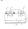
- Figure 1 is a cross section of a first embodiment of a semiconductor apparatus according to the present invention.
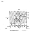
- Figure 2(a) is a cross section for explaining a manufacturing process of p-type impurity doping.
- Figure 2(b) is a cross section for explaining a manufacturing process of n-type impurity doping.
- Figure 3(a) is a top plan view showing a main portion of a second embodiment of a semiconductor apparatus according to the invention.
- Figure 3(b) is a cross section taken along A-A of Figure 3(a).
- Figure 4 is a cross section of the second embodiment including the partial cross section shown in Figure 3(b).
- Figure 5 is a cross section of a third embodiment of a semiconductor apparatus according to the invention.
- Figure 6 is an equivalent circuit diagram of Figure 5.
- Figure 7 is an equivalent circuit diagram of a fourth embodiment of a semiconductor apparatus according to the invention.
- Figure 8 is an equivalent circuit diagram of the semiconductor apparatus of Figure 4 including p-type regions.
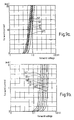
- Figure 9(a) is a set of curves relating the forward voltage of the temperature sensor with the forward current of up to 20 mA with the temperature as a parameter.
- Figure 9(b) is a set of curves relating the forward voltage of the temperature sensor with the forward current of up to 2 mA with the temperature as a parameter.
- Figure 10 is a graph relating the forward voltage with the junction temperature on the bases of the data of Figs. 9(a) and 9(b).
- Figure 1 is a cross section of a first embodiment of a semiconductor apparatus according to the present invention. Referring to Figure 1, this semiconductor apparatus uses a lightly doped n-type substrate 1. After all the pertinent semiconductor regions are formed, n-type substrate 1 turns out to be an n- region 101. A p-type well region 2 is selectively formed in a first surface portion of n-type substrate 1. An n+ emitter region 3 is selectively formed in a surface portion of p-type well region 2.
- a gate electrode 5 is fixed via a gate insulation film 4 to that portion of p-type well region 2 separating n+ emitter region 3 and n- region 101 from each other.
- An emitter electrode 6 is disposed on n+ emitter region 3 and on a central contact region 20 on p-type well region 2.
- a p+ or n+ collector region 7 is disposed on a rear surface (the undersurface as seen in the Figure) of n-type substrate 1.
- a collector electrode 8 is disposed on the collector region 7.
- a p-type anode region 9 is selectively formed in a second surface portion of n-type substrate 1.
- P-type anode region 9 is spaced apart from p-type well region 2 by an area of n- region 101.
- An n-type cathode region 10 is formed in a surface portion of p-type anode region 9.
- An anode electrode 11 is positioned on p-type anode region 9, and a cathode electrode 12 is positioned on n-type cathode region 10.
- P-type anode region 9 and n-type cathode region 10 constitute a pn diode as a temperature sensing element (temperature sensor).
- Cathode electrode 12 is connected to emitter electrode 6, and both are connected to an emitter terminal 13.
- Gate electrode 5 is connected to a gate terminal 14.
- Anode electrode 1 1 is connected to a temperature sensing terminal 15.
- Collector electrode 8 is connected to a collector terminal 16.
- the collector region 7 is a p+ type one, that is when the power device is an IGBT, an npnp quadruple-layered structure (a parasitic thyristor), consisting of n-type cathode region 10, p-type anode region 9, n+ region 101, and p+ collector region 7, is formed.
- a parasitic thyristor a parasitic thyristor
- Figure 2(a) is a schematic cross sectional view for explaining the manufacturing process employing p-type impurity doping.
- Figure 2(b) is a schematic cross section for explaining a manufacturing process employing n-type impurity doping.
- boron (B) ions are selectively implanted into regions of the surface of the substrate 1. Then, the implanted B ions are thermally diffused to simultaneously form the p-type well region 2 and the p-type anode region 9.
- a poly-crystalline silicon film 17 which will be gate electrode 5 is used as an ion implantation mask for forming p-type well region 2.
- a photoresist film 18 is used as an ion implantation masking for forming p-type anode region 9.
- arsenic (As) ions are selectively implanted into regions of the surface of p-type well region 2 and p-type anode region 9 to simultaneously form n+ emitter region 3 and n-type cathode region 10.
- Poly-crystalline silicon film 17 which will be gate electrode 5 and photoresist film 18 are used as an ion implantation masking to define the outline for forming n+ emitter region 3.
- a photoresist film 18 is used as an ion implantation mask for forming n-type cathode region 10.
- the region of the surface which contains n-type cathode region 10 constitutes a temperature sensor.
- Figure 3(a) is a top plan view showing a main portion of a second embodiment of a semiconductor apparatus according to the invention
- Figure 3(b) is a cross section taken along A-A of Figure 3(a).
- An n-type cathode region 10 and a p-type anode region 9 are formed concentrically with each other.
- a p-type region 21 surrounds p-type anode region 9.
- a cathode electrode 12 is formed on the n-type cathode region 10.
- a cathode electrode 12 is connected to an emitter electrode of an IGBT (not shown) via a metal film 22.
- An anode electrode 11 is formed on anode region 9.
- a metal electrode is on p-type region 21.
- Metal film 22 is insulated from anode electrode 11, metal electrode 23, and semiconductor substrate 1 by an inter-layer insulation film (not shown).
- a collector region is omitted from Figure 3(b).
- Figure 4 is a cross section of the second embodiment including the partial cross section shown in Figure 3(b).
- the collector region is omitted from Figure 4.
- Cathode electrode 12, metal electrode 23 and emitter electrode 6 are connected to one another via the metal film 22 shown in Figure 3(a), and also to an emitter terminal 13.
- An anode electrode 11 is connected to a temperature sensing terminal 15. From left to right in the Figure, there are seen an IGBT portion, a p-type region, a temperature sensor, and a further p-type region.
- the left hand side and right hand side of the semiconductor apparatus are shown separately only for the sake of illustration convenience.
- FIG. 5 is a cross section of a third embodiment of a semiconductor apparatus according to the invention.
- the third embodiment connects two pn diodes in series to constitute a temperature sensor.
- a cathode electrode 12 of a first pn diode is connected to an anode electrode 11 of a second pn diode.
- An anode electrode 11 of the first pn diode is connected to a temperature sensing terminal 15.
- a cathode electrode 12 of the second pn diode is connected to an emitter electrode 6.
- a collector region is omitted from Figure 4.
- Three or more pn diodes may be connected in series, to increase the sensitivity of the temperature detection.
- Figure 6 is a circuit diagram of the circuit of Figure 5.
- An anode side of a temperature sensor 50 is connected to temperature sensing terminal 15, and a cathode side thereof to emitter electrode 6.
- FIG. 7 is an equivalent circuit diagram of a fourth embodiment of a semiconductor apparatus according to the invention.
- a constant current supply is also shown in the Figure.
- a semiconductor apparatus 30 is in an area surrounded by broken lines with an IGBT 40 arranged on the left hand side therein.
- a temperature sensor 50 which comprises a pn diode is positioned adjacent to IGBT 40.
- a temperature sensing terminal 15 is connected to a positive electrode of a constant current supply 24, and an emitter terminal 13 to a negative electrode thereof to make a small current flow from an anode of the pn diode to its cathode.
- FIG 8 is an equivalent circuit diagram of the semiconductor apparatus of Figure 4 including p-type regions.
- This Figure shows a constant current supply connected to the semiconductor apparatus.
- An IGBT 40, a p-type region 21, and a temperature sensor 50 are arranged side by side from the left hand side of the Figure.
- parasitic pnp and npn transistors constitute a pnpn parasitic thyristor.
- a constant current supply 24 is connected as shown in Figure 8.
- Another emitter terminal 13a is connected for making a main current flow through IGBT 40. Emitter terminal 13a is indispensable especially when it is necessary to make a very high current flow through the IGBT.
- Figure 9(a) is a set of curves relating the forward voltage of the temperature sensor with the forward current of up to 20 mA with the temperature as a parameter.
- Figure 9(b) is a set of curves relating the forward voltage of the temperature sensor with the forward current of up to 2 mA with the temperature as a parameter.
- the abscissa of Figure 9(a) is divided every 0.2 V, and the abscissa of Figure 9(b) every 0.1 V.
- Figure 10 shows the relationship between the forward voltage and the junction temperature based on the data of Figs. 9(a) and 9(b).
- a current value at which the forward voltage changes greatly with temperatures A current of 0.2 mA (a sensing current value) from the constant current supply is adopted.
- the temperature of the temperature sensor i.e. the IGBT temperature
- the IGBT temperature is 125°C when the forward voltage of the temperature sensor (a detected voltage value) is 0.6 V. Therefore, the IGBT is prevented from breakdown caused by overheating, by operating an external protecting circuit when the forward voltage reaches a predetermined value, 0.6 V for example, so that the IGBT temperature may not exceeds 125°C.
- IPMs exhibiting the same effects with those of the foregoing embodiments may be obtained by using a p-type substrate on which each region is disposed using an opposite conductivity type to that of the foregoing embodiments.
- a temperature sensor is integrated with an IGBT on one semiconductor substrate in the semiconductor apparatus of the invention. Therefore, the IGBT is securely protected against overheating, since the temperature of the IGBT is detected accurately in a short time.
- the effects of the invention are multiplied by connecting multiple pn diodes to constitute a temperature sensor of increased sensitivity.
Landscapes
- Metal-Oxide And Bipolar Metal-Oxide Semiconductor Integrated Circuits (AREA)
- Semiconductor Integrated Circuits (AREA)
- Insulated Gate Type Field-Effect Transistor (AREA)
- Electronic Switches (AREA)
Applications Claiming Priority (2)
| Application Number | Priority Date | Filing Date | Title |
|---|---|---|---|
| JP12331195A JP3168874B2 (ja) | 1995-05-23 | 1995-05-23 | 半導体装置 |
| JP123311/95 | 1995-05-23 |
Publications (2)
| Publication Number | Publication Date |
|---|---|
| EP0744770A2 true EP0744770A2 (fr) | 1996-11-27 |
| EP0744770A3 EP0744770A3 (fr) | 1997-10-22 |
Family
ID=14857413
Family Applications (1)
| Application Number | Title | Priority Date | Filing Date |
|---|---|---|---|
| EP96303575A Withdrawn EP0744770A3 (fr) | 1995-05-23 | 1996-05-20 | Appareil à semi-conducteur |
Country Status (3)
| Country | Link |
|---|---|
| US (1) | US5736769A (fr) |
| EP (1) | EP0744770A3 (fr) |
| JP (1) | JP3168874B2 (fr) |
Cited By (3)
| Publication number | Priority date | Publication date | Assignee | Title |
|---|---|---|---|---|
| CN105258817A (zh) * | 2014-07-11 | 2016-01-20 | 英飞凌科技股份有限公司 | 用于分立半导体器件的集成温度传感器 |
| US10861847B2 (en) | 2016-12-14 | 2020-12-08 | Sony Semiconductor Solutions Corporation | Semiconductor device and protection element |
| DE102019219688B4 (de) | 2018-12-21 | 2024-09-12 | Mitsubishi Electric Corporation | Halbleitervorrichtung und Verfahren zum Herstellen derselben |
Families Citing this family (20)
| Publication number | Priority date | Publication date | Assignee | Title |
|---|---|---|---|---|
| US6133616A (en) * | 1998-10-02 | 2000-10-17 | International Rectifier Corp. | Tempsense FET with implanted line of diodes (EPS) |
| JP4093678B2 (ja) * | 1999-05-11 | 2008-06-04 | 三菱電機株式会社 | 電動機制御装置 |
| DE10042022A1 (de) * | 2000-08-08 | 2002-03-07 | Infineon Technologies Ag | Verfahren und Vorrichtung zur Messung der Temperatur des laseraktiven Bereiches einer Halbleiterlaserdiode |
| JP4620889B2 (ja) * | 2001-03-22 | 2011-01-26 | 三菱電機株式会社 | 電力用半導体装置 |
| US6806772B2 (en) | 2002-11-06 | 2004-10-19 | Itt Manufacturing Enterprises, Inc. | Power transistor array temperature control system |
| JP4097613B2 (ja) * | 2004-03-09 | 2008-06-11 | 三菱電機株式会社 | 半導体装置 |
| JP5028748B2 (ja) * | 2005-04-15 | 2012-09-19 | 富士電機株式会社 | パワー半導体デバイスの温度計測装置 |
| KR100880231B1 (ko) * | 2007-06-20 | 2009-01-28 | 주식회사 동부하이텍 | 반도체 소자 및 그의 제조 방법 |
| JP2009289791A (ja) * | 2008-05-27 | 2009-12-10 | Nec Electronics Corp | 半導体装置 |
| US9520486B2 (en) | 2009-11-04 | 2016-12-13 | Analog Devices, Inc. | Electrostatic protection device |
| US10199482B2 (en) | 2010-11-29 | 2019-02-05 | Analog Devices, Inc. | Apparatus for electrostatic discharge protection |
| US8742455B2 (en) * | 2011-05-11 | 2014-06-03 | Analog Devices, Inc. | Apparatus for electrostatic discharge protection |
| US8816389B2 (en) | 2011-10-21 | 2014-08-26 | Analog Devices, Inc. | Overvoltage and/or electrostatic discharge protection device |
| US8803193B2 (en) | 2011-05-11 | 2014-08-12 | Analog Devices, Inc. | Overvoltage and/or electrostatic discharge protection device |
| US9484739B2 (en) | 2014-09-25 | 2016-11-01 | Analog Devices Global | Overvoltage protection device and method |
| US10181719B2 (en) | 2015-03-16 | 2019-01-15 | Analog Devices Global | Overvoltage blocking protection device |
| JP2017005153A (ja) * | 2015-06-11 | 2017-01-05 | ルネサスエレクトロニクス株式会社 | 半導体装置 |
| JP6508255B2 (ja) * | 2017-05-17 | 2019-05-08 | セイコーエプソン株式会社 | 電気光学装置および電子機器 |
| CN114420561B (zh) * | 2022-03-31 | 2022-07-15 | 深圳市威兆半导体有限公司 | 一种igbt器件及其制造方法 |
| CN114843344B (zh) * | 2022-04-21 | 2025-12-09 | 西安电子科技大学 | 基于新型碳化硅mosfet结构的智能测热芯片及其版图结构 |
Family Cites Families (5)
| Publication number | Priority date | Publication date | Assignee | Title |
|---|---|---|---|---|
| JPS63181376A (ja) * | 1987-01-23 | 1988-07-26 | Toshiba Corp | 半導体装置 |
| GB2204445B (en) * | 1987-03-06 | 1991-04-24 | Texas Instruments Ltd | Semiconductor switch |
| US5049961A (en) * | 1989-01-10 | 1991-09-17 | Ixys Corporation | Monolithic temperature sensing device |
| US4970497A (en) * | 1989-11-22 | 1990-11-13 | Westinghouse Electric Corp. | Method and apparatus for sensing thermal stress in integrated circuits |
| US5313088A (en) * | 1990-09-19 | 1994-05-17 | Nec Corporation | Vertical field effect transistor with diffused protection diode |
-
1995
- 1995-05-23 JP JP12331195A patent/JP3168874B2/ja not_active Expired - Fee Related
-
1996
- 1996-05-20 EP EP96303575A patent/EP0744770A3/fr not_active Withdrawn
- 1996-05-23 US US08/652,115 patent/US5736769A/en not_active Expired - Lifetime
Cited By (4)
| Publication number | Priority date | Publication date | Assignee | Title |
|---|---|---|---|---|
| CN105258817A (zh) * | 2014-07-11 | 2016-01-20 | 英飞凌科技股份有限公司 | 用于分立半导体器件的集成温度传感器 |
| US10712208B2 (en) | 2014-07-11 | 2020-07-14 | Infineon Technologies Ag | Integrated temperature sensor for discrete semiconductor devices |
| US10861847B2 (en) | 2016-12-14 | 2020-12-08 | Sony Semiconductor Solutions Corporation | Semiconductor device and protection element |
| DE102019219688B4 (de) | 2018-12-21 | 2024-09-12 | Mitsubishi Electric Corporation | Halbleitervorrichtung und Verfahren zum Herstellen derselben |
Also Published As
| Publication number | Publication date |
|---|---|
| EP0744770A3 (fr) | 1997-10-22 |
| JP3168874B2 (ja) | 2001-05-21 |
| JPH08316471A (ja) | 1996-11-29 |
| US5736769A (en) | 1998-04-07 |
Similar Documents
| Publication | Publication Date | Title |
|---|---|---|
| US5736769A (en) | Semiconductor apparatus | |
| US11276680B2 (en) | Power semiconductor device with integrated temperature protection | |
| EP0060635B1 (fr) | Circuit intégré semiconducteur contenant un élément de protection | |
| US8089134B2 (en) | Semiconductor device | |
| US9461032B1 (en) | Bipolar ESD protection device with integrated negative strike diode | |
| CN113544846B (zh) | 半导体装置及系统 | |
| JPS6358380B2 (fr) | ||
| EP0315213B1 (fr) | Dispositif MOSFET vertical avec protection | |
| JP3805534B2 (ja) | 半導体集積回路及び保護素子の使用方法 | |
| EP0103306B1 (fr) | Dispositif semi-conducteur de protection | |
| JP7691809B2 (ja) | 半導体装置および半導体装置の製造方法 | |
| US20230143787A1 (en) | Semiconductor device and manufacturing method of semiconductor device | |
| JPH09186329A (ja) | 温度センサを有する電力用半導体デバイス | |
| JP2680788B2 (ja) | 集積化構造の能動クランプ装置 | |
| US5545914A (en) | Semiconductor device having zener diodes with temperature stability between base and collector regions | |
| KR100272052B1 (ko) | 파워 트랜지스터 | |
| KR860000714B1 (ko) | 집적회로 보호장치 | |
| JP2505652B2 (ja) | 低トリガ電圧scr保護装置及び構造 | |
| US5296732A (en) | Bipolar transistor | |
| US5936284A (en) | Electrostatic discharge protection circuit and transistor | |
| JP4018163B2 (ja) | トランジスタの降伏電圧制御用半導体回路装置 | |
| US6777784B1 (en) | Bipolar transistor-based electrostatic discharge (ESD) protection structure with a heat sink | |
| JPH08321588A (ja) | 静電気放電保護回路 | |
| HK1046061A1 (zh) | 集成电路的静电放电保护 | |
| JP2960108B2 (ja) | 過電圧保護機能付半導体素子 |
Legal Events
| Date | Code | Title | Description |
|---|---|---|---|
| PUAI | Public reference made under article 153(3) epc to a published international application that has entered the european phase |
Free format text: ORIGINAL CODE: 0009012 |
|
| AK | Designated contracting states |
Kind code of ref document: A2 Designated state(s): DE FR GB |
|
| PUAL | Search report despatched |
Free format text: ORIGINAL CODE: 0009013 |
|
| AK | Designated contracting states |
Kind code of ref document: A3 Designated state(s): DE FR GB |
|
| 17P | Request for examination filed |
Effective date: 19971114 |
|
| 17Q | First examination report despatched |
Effective date: 20000720 |
|
| STAA | Information on the status of an ep patent application or granted ep patent |
Free format text: STATUS: THE APPLICATION IS DEEMED TO BE WITHDRAWN |
|
| 18D | Application deemed to be withdrawn |
Effective date: 20010926 |