EP0744774A2 - Transistor à effet de champ et son procédé de fabrication - Google Patents
Transistor à effet de champ et son procédé de fabrication Download PDFInfo
- Publication number
- EP0744774A2 EP0744774A2 EP96108283A EP96108283A EP0744774A2 EP 0744774 A2 EP0744774 A2 EP 0744774A2 EP 96108283 A EP96108283 A EP 96108283A EP 96108283 A EP96108283 A EP 96108283A EP 0744774 A2 EP0744774 A2 EP 0744774A2
- Authority
- EP
- European Patent Office
- Prior art keywords
- active layer
- heavily doped
- layer
- field effect
- effect transistor
- Prior art date
- Legal status (The legal status is an assumption and is not a legal conclusion. Google has not performed a legal analysis and makes no representation as to the accuracy of the status listed.)
- Withdrawn
Links
Images


Classifications
-
- H—ELECTRICITY
- H10—SEMICONDUCTOR DEVICES; ELECTRIC SOLID-STATE DEVICES NOT OTHERWISE PROVIDED FOR
- H10D—INORGANIC ELECTRIC SEMICONDUCTOR DEVICES
- H10D30/00—Field-effect transistors [FET]
- H10D30/01—Manufacture or treatment
- H10D30/061—Manufacture or treatment of FETs having Schottky gates
- H10D30/0612—Manufacture or treatment of FETs having Schottky gates of lateral single-gate Schottky FETs
-
- H—ELECTRICITY
- H10—SEMICONDUCTOR DEVICES; ELECTRIC SOLID-STATE DEVICES NOT OTHERWISE PROVIDED FOR
- H10D—INORGANIC ELECTRIC SEMICONDUCTOR DEVICES
- H10D30/00—Field-effect transistors [FET]
- H10D30/60—Insulated-gate field-effect transistors [IGFET]
- H10D30/601—Insulated-gate field-effect transistors [IGFET] having lightly-doped drain or source extensions, e.g. LDD IGFETs or DDD IGFETs
-
- H—ELECTRICITY
- H10—SEMICONDUCTOR DEVICES; ELECTRIC SOLID-STATE DEVICES NOT OTHERWISE PROVIDED FOR
- H10D—INORGANIC ELECTRIC SEMICONDUCTOR DEVICES
- H10D12/00—Bipolar devices controlled by the field effect, e.g. insulated-gate bipolar transistors [IGBT]
- H10D12/01—Manufacture or treatment
- H10D12/031—Manufacture or treatment of IGBTs
- H10D12/032—Manufacture or treatment of IGBTs of vertical IGBTs
- H10D12/038—Manufacture or treatment of IGBTs of vertical IGBTs having a recessed gate, e.g. trench-gate IGBTs
-
- H—ELECTRICITY
- H10—SEMICONDUCTOR DEVICES; ELECTRIC SOLID-STATE DEVICES NOT OTHERWISE PROVIDED FOR
- H10D—INORGANIC ELECTRIC SEMICONDUCTOR DEVICES
- H10D30/00—Field-effect transistors [FET]
- H10D30/01—Manufacture or treatment
- H10D30/021—Manufacture or treatment of FETs having insulated gates [IGFET]
- H10D30/0223—Manufacture or treatment of FETs having insulated gates [IGFET] having source and drain regions or source and drain extensions self-aligned to sides of the gate
- H10D30/0227—Manufacture or treatment of FETs having insulated gates [IGFET] having source and drain regions or source and drain extensions self-aligned to sides of the gate having both lightly-doped source and drain extensions and source and drain regions self-aligned to the sides of the gate, e.g. lightly-doped drain [LDD] MOSFET or double-diffused drain [DDD] MOSFET
-
- H—ELECTRICITY
- H10—SEMICONDUCTOR DEVICES; ELECTRIC SOLID-STATE DEVICES NOT OTHERWISE PROVIDED FOR
- H10D—INORGANIC ELECTRIC SEMICONDUCTOR DEVICES
- H10D30/00—Field-effect transistors [FET]
- H10D30/80—FETs having rectifying junction gate electrodes
- H10D30/87—FETs having Schottky gate electrodes, e.g. metal-semiconductor FETs [MESFET]
- H10D30/877—FETs having Schottky gate electrodes, e.g. metal-semiconductor FETs [MESFET] having recessed gate electrodes
-
- H—ELECTRICITY
- H10—SEMICONDUCTOR DEVICES; ELECTRIC SOLID-STATE DEVICES NOT OTHERWISE PROVIDED FOR
- H10D—INORGANIC ELECTRIC SEMICONDUCTOR DEVICES
- H10D62/00—Semiconductor bodies, or regions thereof, of devices having potential barriers
- H10D62/10—Shapes, relative sizes or dispositions of the regions of the semiconductor bodies; Shapes of the semiconductor bodies
- H10D62/13—Semiconductor regions connected to electrodes carrying current to be rectified, amplified or switched, e.g. source or drain regions
- H10D62/149—Source or drain regions of field-effect devices
- H10D62/161—Source or drain regions of field-effect devices of FETs having Schottky gates
-
- H—ELECTRICITY
- H10—SEMICONDUCTOR DEVICES; ELECTRIC SOLID-STATE DEVICES NOT OTHERWISE PROVIDED FOR
- H10D—INORGANIC ELECTRIC SEMICONDUCTOR DEVICES
- H10D64/00—Electrodes of devices having potential barriers
- H10D64/20—Electrodes characterised by their shapes, relative sizes or dispositions
- H10D64/23—Electrodes carrying the current to be rectified, amplified, oscillated or switched, e.g. sources, drains, anodes or cathodes
- H10D64/251—Source or drain electrodes for field-effect devices
- H10D64/258—Source or drain electrodes for field-effect devices characterised by the relative positions of the source or drain electrodes with respect to the gate electrode
-
- H—ELECTRICITY
- H10—SEMICONDUCTOR DEVICES; ELECTRIC SOLID-STATE DEVICES NOT OTHERWISE PROVIDED FOR
- H10D—INORGANIC ELECTRIC SEMICONDUCTOR DEVICES
- H10D84/00—Integrated devices formed in or on semiconductor substrates that comprise only semiconducting layers, e.g. on Si wafers or on GaAs-on-Si wafers
- H10D84/01—Manufacture or treatment
- H10D84/0123—Integrating together multiple components covered by H10D12/00 or H10D30/00, e.g. integrating multiple IGBTs
- H10D84/0126—Integrating together multiple components covered by H10D12/00 or H10D30/00, e.g. integrating multiple IGBTs the components including insulated gates, e.g. IGFETs
- H10D84/013—Manufacturing their source or drain regions, e.g. silicided source or drain regions
-
- H—ELECTRICITY
- H10—SEMICONDUCTOR DEVICES; ELECTRIC SOLID-STATE DEVICES NOT OTHERWISE PROVIDED FOR
- H10P—GENERIC PROCESSES OR APPARATUS FOR THE MANUFACTURE OR TREATMENT OF DEVICES COVERED BY CLASS H10
- H10P76/00—Manufacture or treatment of masks on semiconductor bodies, e.g. by lithography or photolithography
- H10P76/20—Manufacture or treatment of masks on semiconductor bodies, e.g. by lithography or photolithography of masks comprising organic materials
- H10P76/204—Manufacture or treatment of masks on semiconductor bodies, e.g. by lithography or photolithography of masks comprising organic materials of organic photoresist masks
Definitions
- a GaAs MESFET is generally configured by forming a gate electrode in Schottky contact with an active layer formed on the upper surface of a semi-insulating GaAs substrate and by forming a source electrode and a drain electrode in ohmic contact with the active layer on both sides of the gate electrode.
- a surface depletion layer is generated by surface charge on the surface of the GaAs substrate, which above-described configuration is unable to provide excellent increases parasitic resistance and reduces both mutual conductance g m in high frequency bands and a current gain cut-off frequency f T . Therefore, a GaAs MESFET having the high frequency characteristics and is limited in applicability to high power use.
- an offset gate structure in which a distance between the gate electrode and the drain electrode is greater than that between the gate electrode and source electrode to prevent an electric field from concentrating at an edge of the gate electrode on the side toward the drain electrode.
- a step recess structure in which a recess is formed at the bottom of another recess to formed stepped side faces.
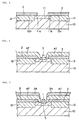
- Fig. 1 is a sectional view of a field effect transistor of a first embodiment of the present invention.
- Fig. 10 is a sectional view of the semiconductor substrate 10 on which ion implantation is carried out after forming side walls 49a and 49b on the sides of the SiO 2 film 48 in a step of manufacturing the field effect transistor 22 of the second embodiment.
- Fig. 12 is a sectional view of a field effect transistor 24 of a fourth embodiment of the present invention.
- the source electrode 2 is formed on the surface 12a of the heavily doped layer 12 and the surface 11a of the active layer 11, and this forms ohmic contact between the source electrode 2 and the heavily doped layer 12 and ohmic contact between the source electrode 2 and the active layer 11.
- the surface 11a of the active layer 11 is a portion having a predetermined width L2 along the surface of the active layer 11 which extends along the boundary between the active layer 11 and the heavily doped layer 12.
- the drain electrode 3 is formed on the surface 13a of the heavily doped layer 13 and the surface 11b of the active layer 11, and this forms ohmic contact between the drain electrode 3 and the heavily doped layer 13 and ohmic contact between the drain electrode 3 and the active layer 11.
- the surface 11b of the active layer 11 is a portion having a predetermined width L3 along the surface of the active layer 11 which extends along the boundary between the active layer 11 and the heavily doped layer 13.
- the heavily doped layer 12 has an impurity concentration higher than that of the active layer 11, contact resistance between the heavily doped layer 12 and the source electrode 2 at the surface 12a of the heavily doped layer 12 is lower than contact resistance between the active layer 11 and the source electrode 2 at the surface 11a of the active layer 11.
- the heavily doped layer 13 has an impurity concentration higher than that of the active layer 11, contact resistance between the heavily doped layer 13 and the drain electrode 3 at the surface 13a of the heavily doped layer 13 is lower than contact resistance between the active layer 11 and the drain electrode 3 at the surface 11b of the active layer 11.
- the field effect transistor 21 of the first embodiment is configured as described above.
- an active layer 11 having an impurity concentration equal to the impurity concentration of the n-type semiconductor layer 31 is remained directly under the photo resist 45, and heavily doped layers 12 and 13 having an impurity concentration higher than the impurity concentration of the n-type semiconductor layer 31 are formed on both sides of the active layer 11.
- an aluminum film is deposited using a vacuum deposition process from above the semiconductor substrate 10 so as to form a film 34 on the photo resist 47 and form a film in the recess 5 as a gate electrode 1.
- the film 34 and the photo resist 47 are removed by a lift-off method.
- the field effect transistor 21 of the first embodiment is manufactured through the above-described steps.
- a voltage drop of a voltage Vgd i.e., a voltage between the gate electrode 1 and the drain electrode 3 during the operation of the field effect transistor 21
- a voltage drop of the voltage Vgd caused by the contact resistance between the drain electrode 3 and the active layer 11 is greater than a voltage drop of the voltage Vgd caused by the contact resistance between the drain electrode 3 and the heavily doped layer 13.
- the high electrical field in the heavily doped layer 113 in the vicinity of the electrode edge portion 103 of the prior art is delocalized to be in those two locations, i.e., the electrode edge portion 3a and the boundary portion 3b.
- Fig. 8 is a sectional view of a field effect transistor 22 of a second embodiment of the present invention.
- the same components as those in the field effect transistor 21 in Fig. 1 are indicated by the same reference numbers.
- the field effect transistor 22 of the second embodiment shown in Fig. 8 is different from the field effect transistor 21 of the first embodiment shown in Fig. 1 on the following points.
- the gate breakdown voltage can be further improved compared to a case wherein the recess 5 is formed. That is, in the field effect transistor 23 shown in Fig. 9, the drain breakdown voltage can be improved just as in the first embodiment, and the gate breakdown voltage can be further improved compared to the first embodiment.
- each of the electrical fields in the active layer 11 and the heavily doped layers 12 and 13 is distributed to the step portion 12d including a step portion upper end 2c and a step portion lower end 2d and the step portion 13d including a step portion upper end 3c and a step portion lower end 3d.
- high electrical fields in the vicinity of the electrode edge portions 2a and 3a can be further relieved compared to those in the field effect transistor 21 of the first embodiment. That is, in the field effect transistor 24 of the fourth embodiment, the source breakdown voltage and the drain breakdown voltage can be further improved compared to those in the field effect transistor 21.
- step portion is provided at the heavily doped layers 12 and 13 in the above-described second embodiment
- the present invention is not limited thereto, and a step portion may be provided in at least one of the heavily doped layers 12 and 13.
- Such a configuration also results in the same improvements and effects as in the second embodiment and allows the source breakdown voltage or drain breakdown voltage to be further improved compared to a case wherein no step portion is provided.
Landscapes
- Junction Field-Effect Transistors (AREA)
Applications Claiming Priority (2)
| Application Number | Priority Date | Filing Date | Title |
|---|---|---|---|
| JP7126385A JPH08321512A (ja) | 1995-05-25 | 1995-05-25 | 電界効果トランジスタとその製造方法 |
| JP126385/95 | 1995-05-25 |
Publications (2)
| Publication Number | Publication Date |
|---|---|
| EP0744774A2 true EP0744774A2 (fr) | 1996-11-27 |
| EP0744774A3 EP0744774A3 (fr) | 1998-01-28 |
Family
ID=14933844
Family Applications (1)
| Application Number | Title | Priority Date | Filing Date |
|---|---|---|---|
| EP96108283A Withdrawn EP0744774A3 (fr) | 1995-05-25 | 1996-05-23 | Transistor à effet de champ et son procédé de fabrication |
Country Status (3)
| Country | Link |
|---|---|
| EP (1) | EP0744774A3 (fr) |
| JP (1) | JPH08321512A (fr) |
| KR (1) | KR960043276A (fr) |
Family Cites Families (5)
| Publication number | Priority date | Publication date | Assignee | Title |
|---|---|---|---|---|
| US4336549A (en) * | 1978-02-21 | 1982-06-22 | Hughes Aircraft Company | Schottky-barrier gate gallium arsenide field effect devices |
| GB1602498A (en) * | 1978-05-31 | 1981-11-11 | Secr Defence | Fet devices and their fabrication |
| JPS57199221A (en) * | 1981-06-02 | 1982-12-07 | Toshiba Corp | Manufacture of semiconductor device |
| JPS62188380A (ja) * | 1986-02-14 | 1987-08-17 | Nec Corp | 電界効果トランジスタ |
| JPH023938A (ja) * | 1988-06-20 | 1990-01-09 | Mitsubishi Electric Corp | 電界効果トランジスタ |
-
1995
- 1995-05-25 JP JP7126385A patent/JPH08321512A/ja active Pending
-
1996
- 1996-05-23 EP EP96108283A patent/EP0744774A3/fr not_active Withdrawn
- 1996-05-23 KR KR1019960017754A patent/KR960043276A/ko not_active Abandoned
Also Published As
| Publication number | Publication date |
|---|---|
| JPH08321512A (ja) | 1996-12-03 |
| EP0744774A3 (fr) | 1998-01-28 |
| KR960043276A (ko) | 1996-12-23 |
Similar Documents
| Publication | Publication Date | Title |
|---|---|---|
| US5510280A (en) | Method of making an asymmetrical MESFET having a single sidewall spacer | |
| US4803526A (en) | Schottky gate field effect transistor and manufacturing method | |
| US4698654A (en) | Field effect transistor with a submicron vertical structure and its production process | |
| US5187379A (en) | Field effect transistor and manufacturing method therefor | |
| US3983572A (en) | Semiconductor devices | |
| KR950007361B1 (ko) | 전계효과트랜지스터 | |
| US5824575A (en) | Semiconductor device and method of manufacturing the same | |
| US5837570A (en) | Heterostructure semiconductor device and method of fabricating same | |
| EP0744774A2 (fr) | Transistor à effet de champ et son procédé de fabrication | |
| EP0498993B1 (fr) | Transistor à effet de champ et sa méthode de production | |
| US5389807A (en) | Field effect transistor | |
| JPS5979577A (ja) | 半導体集積回路装置 | |
| JP3653652B2 (ja) | 半導体装置 | |
| JP2762919B2 (ja) | 半導体素子 | |
| JPH05235045A (ja) | 電界効果トランジスタ | |
| US4694563A (en) | Process for making Schottky-barrier gate FET | |
| US6051455A (en) | Method of making plurality of FETs having different threshold values | |
| EP0121997B1 (fr) | Transistor à effet de champ Schottky et procédé de sa fabrication | |
| JP2893776B2 (ja) | 半導体装置の製造方法 | |
| JPH043102B2 (fr) | ||
| JPH06260510A (ja) | 電界効果型トランジスタおよびその製造方法 | |
| KR950000155B1 (ko) | 전계효과 트랜지스터의 제조방법 | |
| JPH0648839Y2 (ja) | 半導体装置 | |
| KR950003076Y1 (ko) | 화합물 반도체장치 | |
| JP2000150540A (ja) | 電界効果トランジスタ |
Legal Events
| Date | Code | Title | Description |
|---|---|---|---|
| PUAI | Public reference made under article 153(3) epc to a published international application that has entered the european phase |
Free format text: ORIGINAL CODE: 0009012 |
|
| 17P | Request for examination filed |
Effective date: 19960523 |
|
| AK | Designated contracting states |
Kind code of ref document: A2 Designated state(s): DE FI FR GB |
|
| PUAL | Search report despatched |
Free format text: ORIGINAL CODE: 0009013 |
|
| AK | Designated contracting states |
Kind code of ref document: A3 Designated state(s): DE FI FR GB |
|
| 17Q | First examination report despatched |
Effective date: 19980318 |
|
| STAA | Information on the status of an ep patent application or granted ep patent |
Free format text: STATUS: THE APPLICATION IS DEEMED TO BE WITHDRAWN |
|
| 18D | Application deemed to be withdrawn |
Effective date: 19980729 |