EP0746106A2 - Eingabe-/Ausgabeleitweglenkung in einem programmierbaren Feld - Google Patents
Eingabe-/Ausgabeleitweglenkung in einem programmierbaren Feld Download PDFInfo
- Publication number
- EP0746106A2 EP0746106A2 EP96480063A EP96480063A EP0746106A2 EP 0746106 A2 EP0746106 A2 EP 0746106A2 EP 96480063 A EP96480063 A EP 96480063A EP 96480063 A EP96480063 A EP 96480063A EP 0746106 A2 EP0746106 A2 EP 0746106A2
- Authority
- EP
- European Patent Office
- Prior art keywords
- interface
- buses
- multiplexer
- programmable
- array
- Prior art date
- Legal status (The legal status is an assumption and is not a legal conclusion. Google has not performed a legal analysis and makes no representation as to the accuracy of the status listed.)
- Withdrawn
Links
Images




Classifications
-
- H—ELECTRICITY
- H03—ELECTRONIC CIRCUITRY
- H03K—PULSE TECHNIQUE
- H03K19/00—Logic circuits, i.e. having at least two inputs acting on one output; Inverting circuits
- H03K19/02—Logic circuits, i.e. having at least two inputs acting on one output; Inverting circuits using specified components
- H03K19/173—Logic circuits, i.e. having at least two inputs acting on one output; Inverting circuits using specified components using elementary logic circuits as components
- H03K19/177—Logic circuits, i.e. having at least two inputs acting on one output; Inverting circuits using specified components using elementary logic circuits as components arranged in matrix form
- H03K19/17736—Structural details of routing resources
-
- H—ELECTRICITY
- H03—ELECTRONIC CIRCUITRY
- H03K—PULSE TECHNIQUE
- H03K19/00—Logic circuits, i.e. having at least two inputs acting on one output; Inverting circuits
- H03K19/02—Logic circuits, i.e. having at least two inputs acting on one output; Inverting circuits using specified components
- H03K19/173—Logic circuits, i.e. having at least two inputs acting on one output; Inverting circuits using specified components using elementary logic circuits as components
- H03K19/1733—Controllable logic circuits
- H03K19/1737—Controllable logic circuits using multiplexers
-
- H—ELECTRICITY
- H03—ELECTRONIC CIRCUITRY
- H03K—PULSE TECHNIQUE
- H03K19/00—Logic circuits, i.e. having at least two inputs acting on one output; Inverting circuits
- H03K19/02—Logic circuits, i.e. having at least two inputs acting on one output; Inverting circuits using specified components
- H03K19/173—Logic circuits, i.e. having at least two inputs acting on one output; Inverting circuits using specified components using elementary logic circuits as components
- H03K19/177—Logic circuits, i.e. having at least two inputs acting on one output; Inverting circuits using specified components using elementary logic circuits as components arranged in matrix form
- H03K19/17704—Logic circuits, i.e. having at least two inputs acting on one output; Inverting circuits using specified components using elementary logic circuits as components arranged in matrix form the logic functions being realised by the interconnection of rows and columns
Definitions
- This invention relates in general to integrated circuit devices, and, more specifically, to programmable integrated circuit devices having a plurality of programmable logic cells, a programmable interconnection network, and a programmable I/O network.
- Programmable integrated circuits are known in the art and include programmable logic devices ("PLDs”), Programmable Array Logic (“PALs”), and Programmable Logic Arrays (“PLAs”). Each of these programmable circuits provides an input AND logic plane followed by an OR logic plane. An output function can thus be calculated which is the sum of the products of the input terms.
- the logic planes are usually programmable such that the initial general layout of the planes may be customized for a particular application.
- a more general approach to programmable circuits involves providing an array of distinct, uncommitted logic cells in a Programmable Gate Array ("PGA").
- PGA Programmable Gate Array
- a programmable interconnect network is usually provided to interconnect the cells, and to provide data input to, and output from, the array.
- Customization or programming of the otherwise generally-designed logic cells and interconnect network is performed for a particular application.
- One such array is a Mask Programmable Gate Array (“MPGA”), wherein the configuration of the cells and the wiring network occurs when adding the final layers of metallization to an integrated circuit.
- MPGA Mask Programmable Gate Array
- a modified approach involves the use of laser-directed energy to customize the metallization pattern.
- FPGA Field Programmable Gate Array
- logic cells positioned along the perimeter of the array are committed to providing an interface between a single I/O terminal and the remainder of the array. This is generally a use of these cells for which they were not designed. The numerous resources of certain "high-function" cells are wasted if the cell as a whole is dedicated to an I/O function.
- routing a signal path between interior logic cells and the particular logic cell associated with a desired I/O terminal can present difficulties. For example, if a logic cell in a given array row is committed to the desired I/O terminal, the signal path must be aligned to that particular logic cell. This is a routing constraint that adversely affects the overall flexibility of the array.
- I/O system which provides advanced I/O capability to satisfy the requirements related to higher logic cell densities.
- the I/O system should conserve the logic cell resources of the programmable array and provide additional, programmable routing alternatives near the perimeter of the array.
- the present invention in one aspect, comprises a programmable array having a plurality of programmable logic cells arrayed therein and a programmable interconnect network.
- the programmable interconnect network includes a first plurality of buses wherein selected buses of the first plurality of buses are connectable to ones of the plurality of logic cells.
- the first plurality of buses includes a plurality of switches, each switch of the plurality of switches for programmably providing signals between buses of the first plurality of buses.
- a first I/O interface is associated with a corresponding one of the plurality of logic cells, and includes a data output path, a data input path, a first multiplexer having an output connected to the data output path and a plurality of inputs, and a second multiplexer having an input connected to the data input path and a plurality of outputs.
- the I/O interface includes first and second I/O signal buses, the first I/O signal bus being connected between one of the switches of the first plurality of buses and one of the plurality of inputs to the first multiplexer, the second I/O signal bus being connected between one of the switches of the first plurality of buses and one of the plurality of outputs of the second multiplexer.
- the programmable array may further include a plurality of I/O routing buses running proximate the first I/O interface, at least one of the plurality of I/O buses being programmably connectable to at least one of the first and second I/O signal buses of the first I/O interface.
- the programmable array may further include a programmable element connected between the at least one of the plurality of I/O buses and one of the first and second I/O signal buses of the first I/O interface.
- the plurality of I/O routing buses may run generally along a perimeter of the array.
- the first I/O interface of the programmable array may further include an enable path such that array output signals can be controllably provided to an I/O terminal corresponding to the first I/O interface.
- the I/O interface further includes a third multiplexer having an output connected to the enable path and a plurality of inputs, and a third I/O signal bus, the third I/O signal bus being connected between one of the switches of the first plurality of buses and one of the plurality of inputs of the third multiplexer.
- an I/O and interconnect system for a programmable array having a plurality of programmable logic cells.
- the I/O and interconnect system comprises an I/O terminal, an I/O interface corresponding to the I/O terminal, and a first multiplexer.
- the system further includes a general interconnect network for interconnecting a plurality of logic cells, the general interconnect network including a first plurality of parallel interconnect buses, the first plurality of parallel interconnect buses including a first extended bus connected to the first multiplexer of the I/O interface.
- the system further includes a plurality of perimeter buses running along the perimeter of the array, at least one of the plurality of perimeter buses being programmably connectable to the extended bus of the first plurality of parallel interconnect buses.
- the I/O interface may further include an output path wherein the first multiplexer has an output connected to the output path, an input path, a second multiplexer wherein the second multiplexer has an input connected to the input path, an output enable path, and a third multiplexer wherein the third multiplexer has an output connected to the output enable path.
- the first plurality of parallel interconnect buses may further include second and third extended buses being connected to an output of the second and third multiplexers of the I/O interface, respectively. Selected buses of the plurality of perimeter buses are programmably connectable to a selected one of the first, second and third extended buses of the first plurality of parallel interconnect buses.
- At least one of the plurality of programmable logic cells may include a direct connect output conductor connected to an input of the first multiplexer of the I/O interface, and a direct connect input conductor connected to the input path of the I/O interface.
- Each of the first, second and third extended buses of the first plurality of parallel interconnect buses may be connected to the first, second and third multiplexers of the I/O interface.
- a programmable array having a plurality of logic cells arranged in rows and columns therein including a plurality of perimeter logic cells.
- a programmable interconnect network is provided for interconnecting logic cells of the plurality of logic cells and comprises a plurality of buses, at least some of the plurality of buses being connectable to respective ones of the plurality of logic cells.
- the programmable array further comprises a routing network disposed at the perimeter of the array comprising a plurality of buses.
- a plurality of I/O interfaces are provided about the perimeter of the array such that each of a portion of the plurality of perimeter logic cells has two I/O interfaces corresponding thereto.
- a plurality of first conductors are provided for programmably connecting at least some of the plurality of I/O interfaces to corresponding logic cells about the perimeter of the array.
- a plurality of second conductors are provided for programmably connecting at least some of the plurality of I/O interfaces to corresponding ones of the plurality of buses of the programmable interconnect network, and a plurality of programmable connections for programmably connecting at least some of the plurality of buses of the routing network to at least some of the plurality of second conductors are also provided.
- At least some of the plurality of I/O interfaces of the programmable array may include an output path, an input path and an output enable path.
- a first multiplexer is provided and is connected to the output enable path for programmably selecting signals from a first and second conductor corresponding to the respective I/O interface.
- a second multiplexer is provided and is connected to the output path for programmably selecting signals from a first and second conductor corresponding to the respective I/O interface.
- a third multiplexer is connected to the input path for programmably applying a signal from the input path to a respective one of the plurality of second conductors.
- the routing network may comprise a plurality of programmable switches, at least some of the plurality of programmable switches being programmable to provide signals between respective ones of the plurality of buses of the routing network.
- the routing network includes sixteen buses disposed about the entire perimeter of the array.
- the present invention provides an enhanced I/O capability which satisfies requirements related to higher logic cells densities.
- the I/O system of the present invention conserves logic cell resources of the programmable array and provides additional, programmable routing alternatives near the perimeter of the array.
- a layout of an integrated circuit programmable gate array 10 comprising a plurality of programmable logic cells 12.
- the plurality of programmable logic cells comprises a 56 x 56 array of cells divided into sectors of cells, wherein each sector is defined by an 8 x 8 group of cells.
- the programmable logic cells of the array can be implemented according to the above-incorporated portions of the U.S. Patent application entitled “PROGRAMMABLE LOGIC CELL,” or can be any type of known logic cells, including AND/OR macrocells as in PALs or PLAs.
- I/O input/output
- the position of the I/O interfaces is not necessarily limited to the perimeter of the array.
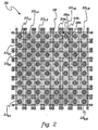
- FIG. 2 there is shown a single sector 20 of programmable logic cells of the array of Fig. 1 .
- a single sector comprises logic cells 22 1,1 to 22 8,8 .
- logic cell 22 1,6 the cell is shown generally surrounded by vertical interconnect buses 24a and 24b, and horizontal interconnect buses 26a and 26b. These horizontal and vertical interconnect buses are positioned between each row and column of the array and provide connections between any two logic cells in the array, or between any logic cell in the array and the I/O interfaces.
- a bus represents a single conductor or a group of conductors, generally co-linerally arranged, which may be interrupted by programmable interconnect elements or repeaters.
- the interconnect buses together form the overall programmable interconnect network of the programmable array.
- Programmable resources within the interconnect network may be provided in addition to those in the programmable logic cells.
- the programmable resources in the interconnect network may include, for example, switches 28 which allow signals to be selectively transmitted between two vertical buses.
- bus turns (not shown) may be employed to provide programmable interconnections between a specified vertical and a specified horizontal interconnect bus.
- the programmable interconnect network can be implemented according to the above-incorporated portions of the U.S. Patent application entitled "PROGRAMMABLE ARRAY INTERCONNECT NETWORK.”
- Fig. 3 depicts the programmable array 10 of Fig. 1 , with certain inventive features thereof emphasized.
- the array 10 may comprise a 7 x 7 arrangement of sectors 32. (Each sector comprises an 8 x 8 arrangement of logic cells.)
- vertical interconnect buses 34a and 34b and horizontal interconnect buses 35a and 35b are depicted. These interconnect buses correspond to buses 24 of Fig. 2 for the perimeter rows and columns of logic cells of the array shown in Fig. 3 .
- an I/O routing network comprising sets 48 of buses is provided at the perimeter of the array 10.
- an additional network of bussing is provided about the perimeter of the array.
- Programmable switches 38 and 40 can be placed at the corners or at the interior of the buses of the I/O routing network, respectively.
- the switches facilitate the communication between ones of the buses within the I/O routing network. Note also, as in the case of buses 36, that switches are not necessary, and that buses could span the entire array (or any portion thereof), uninterrupted. In a preferred embodiment, switches are provided for all of the buses at sector boundaries.
- the programmable I/O routing network of the present invention facilitates communication between interior logic cells, and between interior logic cells and the numerous I/O interfaces (not shown) disposed about the perimeter of the array.
- Fig. 4 depicts a preferred embodiment of the invention in which a perimeter logic cell 64 has two I/O interfaces 44a and 44b associated therewith.
- Buses 50a, 50b and 51 comprise bus sets normally associated with the row and column of logic cell 64.
- Programmable connections or bus turns 68 can be provided between buses 51 and 50.
- I/O routing buses 48 comprising an I/O routing network are disposed generally between the perimeter core cell 64 and the I/O interfaces 44a and 44b.
- buses any arrangement of buses, i.e., in multiple metallization layers of an integrated circuit chip, would fall within the scope of the invention if the depicted connections and related functions are provided thereby.
- sixteen such buses are arranged in eight sets of two buses each, each set of buses having associated therewith periodic switching repeaters 42a-h for providing signals between the buses of each set.
- I/O signal buses 70a-b, 72a-b, and 74a-b are provided and form intersections with buses 48.
- programmable elements 90 e.g., bus turns
- I/O signal buses 70, 72 and 74 can connect directly into the programmable interconnect network via switches 76a-b, 78a-b, and 80a-b, although the switches can be eliminated in other embodiments.
- connections to each respective I/O interface 44 are accomplished via multiplexers 52a-b, 54a-b, and 56a-b, as discussed below.
- Each I/O interface 44 can comprise a respective terminal 46, enable path 62, output path using buffer 58, and input path using buffer 60.
- I/O denotes an input capability, an output capability or both an input and an output capability.
- multiplexers 52, 54 and 56 provide a flexible signal selection scheme such that a signal on any of the respective buses 70, 72 and 74 can be provided to enable paths 62 or data output paths 58.
- any signal received at terminal 46 can be provided to any of the three respective buses 70, 72 and 74 via multiplexer 56.
- each intersection 90 could comprise a pass transistor, an EPROM, a fusible link or an antifuse which affects the desired isolation or connection between the conductors at the intersections.
- a user upon requiring a connection at any particular intersection, would then only be required to perform the proper programming to effect the connection.
- a laser-programmed device could also employ optional welds at the intersection. The required connections are provided by either including or excluding the weld.
- a mask-programmed device would simply include or omit the relevant connections.
- connection broadly denotes either a direct, conductive connection between conductors, or an indirect (e.g., buffered/inverted) interface in which the information from one conductor is nevertheless supplied to the other conductor.
- an "input” or an “output” denotes either a direct or indirect (e.g., buffered/inverted) interface, unless otherwise expressly indicated.
- pass gate multiplexers and bus turns are employed which are controlled by static random access memory (“SRAM”) cells.
- SRAM cells are directly or indirectly (through decoders) tied to the gates of the pass gates within a pass gate multiplexer, thus controlling the state of the pass gates.
- the I/O interface 44a comprises multiplexer 52a.
- a single connection is routed from each potential input bus into the source/drain combination of a field effect transistor transmission gate, and the drain/source combination of the transmission gate is routed to the enable path 62a of the I/O interface.
- Six such transmission gates may be found in this 6:1 pass gate multiplexer and software and decoding logic of the programming system ensures that only one particular pass gate is connected to any single input node.
- each perimeter logic cell maintains direct connections to its corresponding pair of I/O interfaces 44, in addition to at least a connection to the buses 51 of the programmable interconnect network via access points 92. Connections (not shown) to buses 50 are also provided for perimeter logic cell 64.
- Fig. 5 depicts additional detail of the interface of buses 50a-b of the programmable interconnect network and buses 70, 72 and 74 which connect to the I/O interface multiplexers.
- Buses within groups 50a and 50b comprise local ("L"), express ("E") or super ("S") buses.
- L local
- E express
- S super
- the uses of these buses within the array is described in detail in the above-incorporated portions of the U.S. Patent application entitled “PROGRAMMABLE ARRAY INTERCONNECT NETWORK.”
- the local buses are employed to carry signals to and from logic cells.
- the express and super buses comprise longer length conductors and do not generally connect to logic cells, however, they can connect to the local buses via switches such as 78 and 80.
- the super buses span the entire length of the array, thereby offering a virtual terminal capability to the I/O terminal 46 via multiplexers 56, buses 72, and switches 78 (of Fig. 4 ).
- a perimeter logic cell 64 has associated therewith two sets of buses 50a and 50b. Within each set near the perimeter, switches 76a-b, 78a-b and 80a-b are provided. In the preferred embodiment, these switches comprise switching repeaters in which a receive signal is buffered and redriven in a user-selected direction. A switching repeater is described in greater detail below with respect to Fig. 8 . Near the perimeter of the array, ports of the switching repeaters are occupied by conductors 70, 72 and 74 which are applied to the perimeter I/O interfaces, and which form intersections with the buses 48 of the I/O routing network. Thus, signals on buses 50 can be provided either to the I/O interfaces, or to the I/O routing network via conductors 70, 72 and 74.
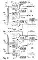
- Fig. 6 depicts greater detail of the connections between conductors 70, 72 and 74 and I/O interfaces 44a and 44b.
- each of the three exemplary paths of each I/O interface i.e., enable, data in, and receiver out
- Conductors 70, 72 and 74 are each connected to each of the multiplexers pursuant to the principles of the present invention.
- direct connect conductors 82, 84, 86 and 88 are connected either to the multiplexers or directly to the receiver out data paths. These conductors run directly to the associated perimeter logic cell. It should be understood that any portion, possibly including all, of the perimeter logic cells may have the two I/O interfaces associated therewith, including the relevant connections. Similarly, any portion, possibly including all, of the I/O interfaces may be designed and connected as discussed above.
- multiplexers 52, 54 and 56 are controlled using SRAM cells. These memory cells, 94, 96 and 98 (and designated M1-M8) are connected (directly or indirectly) to the select inputs of the multiplexers and contain user programming information.
- the CFG and CTS signals applied to the data and enable paths, respectively, provide configuration or test capability.
- the inputs 99 comprise clock, reset, config and test inputs which can also alternatively be processed by I/O interfaces 44.
- Fig. 7 depicts the conditions at any one of the four corners of the array.
- a perimeter logic cell 100 is depicted and has associated therewith I/O interfaces 102a and 102b, and 104a and 104b.
- I/O routing network buses 48 are shown projecting toward the corner and the pattern of switches in each sector is, in fact, continued at the corner of the array. Switches 106a-h are thus provided at the corners of the array pursuant to the principles of the present invention.
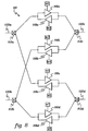
- Fig. 8 depicts a switching repeater 110 employed in the programmable interconnect network and the I/O routing network of a preferred embodiment of the present invention (for example, for switches 76, 78, 80 and 42 of Fig. 4 ).
- the switching repeater buffers and re-drives signals to/from lines 120a-d connected to ports 112a-d.
- directional tri-state buffers 116a-116d and 118a-118d are employed and are controlled by memory cells M1-M8. It will be apparent to one of ordinary skill in the art that an incoming signal on any one of the signal lines 120 can be applied to one, and possibly two, of the remaining signal lines 120. It is also possible that simple non-programmable buffers may be placed in series in any of the buses described above for signal amplification.
- Mask programming techniques include customizing the deposition of the final layers of metallization of an otherwise generally designed integrated circuit (see, for example, U.S. Patent No. 3,993,919 to Cox et al. entitled “PROGRAMMABLE LATCH AND OTHER CIRCUITS FOR LOGIC ARRAYS,” November 23, 1976; and U.S. Patent No. 4,742,383 to Fitzgerald entitled “MULTI-FUNCTION FET MASTERSLICE CELL,” May 3, 1988; both patents assigned to the same assignee as the present application).
- EPROM Erasable programmable read only memory
- EEPROM electrically erasable programmable read only memory
- EPROMS and EEPROMS are both electrically programmable and hold their states, even if power is removed. Special erase procedures can be used, however, to reconfigure the devices (see, for example, Wood et al., "AN ELECTRICALLY ALTERABLE PLA FOR FAST TURNAROUND TIME VLSI DEVELOPMENT HARDWARE," IEEE Journal of Solid-State Circuits, Vol. SC-16, No.
- RAM volatile random access memory
- programming the multiplexers, switching repeaters and bus turns of a preferred embodiment of the present invention involves SRAM cells, programmed by a user.
- Figs. 6 and 8 depict preferred connections for SRAM cells M.
- the array SRAM cells can be configured in accordance with the techniques disclosed in the publication entitled "APPLICATION NOTE AT6000 SERIES CONFIGURATION,” May 1993, Revision 1B, Atmel Corporation, which is hereby incorporated herein by reference in its entirety.
- the present invention provides two flexible I/O interfaces per perimeter core cell, and each I/O interface includes a highly programmable multiplexing system for connecting to the general interconnect network, or to the corresponding perimeter core cell.
- an I/O routing network is provided having a plurality of switches, and which can be programmably connected to intersecting conductors.
- I/O bound signals originating from the interior of the array can be simply routed to the nearest edge, and the I/O routing network of the present invention can be used to apply the signal to any of the numerous I/O interfaces. This signal routing thus increases routing flexibility and avoids the use of perimeter logic cells. Thus, the present invention satisfies the need for advanced I/O capability, conserves perimeter cell resources, and provides flexible routing alternatives about the perimeter of the array.
Landscapes
- Physics & Mathematics (AREA)
- Mathematical Physics (AREA)
- Engineering & Computer Science (AREA)
- Computer Hardware Design (AREA)
- Computing Systems (AREA)
- General Engineering & Computer Science (AREA)
- Computer Networks & Wireless Communication (AREA)
- Logic Circuits (AREA)
- Design And Manufacture Of Integrated Circuits (AREA)
Applications Claiming Priority (2)
| Application Number | Priority Date | Filing Date | Title |
|---|---|---|---|
| US08/460,420 US5671432A (en) | 1995-06-02 | 1995-06-02 | Programmable array I/O-routing resource |
| US460420 | 1995-06-02 |
Publications (2)
| Publication Number | Publication Date |
|---|---|
| EP0746106A2 true EP0746106A2 (de) | 1996-12-04 |
| EP0746106A3 EP0746106A3 (de) | 1997-11-19 |
Family
ID=23828636
Family Applications (1)
| Application Number | Title | Priority Date | Filing Date |
|---|---|---|---|
| EP96480063A Withdrawn EP0746106A3 (de) | 1995-06-02 | 1996-05-07 | Eingabe-/Ausgabeleitweglenkung in einem programmierbaren Feld |
Country Status (3)
| Country | Link |
|---|---|
| US (1) | US5671432A (de) |
| EP (1) | EP0746106A3 (de) |
| JP (1) | JP3372755B2 (de) |
Cited By (8)
| Publication number | Priority date | Publication date | Assignee | Title |
|---|---|---|---|---|
| US5821776A (en) * | 1997-01-31 | 1998-10-13 | Actel Corporation | Field programmable gate array with mask programmed analog function circuits |
| EP1005162A3 (de) * | 1998-11-26 | 2003-04-02 | International Business Machines Corporation | Schaltung und Verfahren zum Erzeugen kombinatorischer logischer Funktionen |
| WO2004088502A3 (de) * | 2003-04-04 | 2005-01-13 | Pact Xpp Technologies Ag | Verfahren und vorrichtung für die datenverarbeitung |
| US7584390B2 (en) | 1997-12-22 | 2009-09-01 | Pact Xpp Technologies Ag | Method and system for alternating between programs for execution by cells of an integrated circuit |
| US9037807B2 (en) | 2001-03-05 | 2015-05-19 | Pact Xpp Technologies Ag | Processor arrangement on a chip including data processing, memory, and interface elements |
| US9047440B2 (en) | 2000-10-06 | 2015-06-02 | Pact Xpp Technologies Ag | Logical cell array and bus system |
| US9075605B2 (en) | 2001-03-05 | 2015-07-07 | Pact Xpp Technologies Ag | Methods and devices for treating and processing data |
| EP3790196A1 (de) * | 2019-09-05 | 2021-03-10 | PatForce GmbH | Switchbox |
Families Citing this family (74)
| Publication number | Priority date | Publication date | Assignee | Title |
|---|---|---|---|---|
| US5367208A (en) | 1986-09-19 | 1994-11-22 | Actel Corporation | Reconfigurable programmable interconnect architecture |
| US6130550A (en) * | 1993-01-08 | 2000-10-10 | Dynalogic | Scaleable padframe interface circuit for FPGA yielding improved routability and faster chip layout |
| US6002268A (en) * | 1993-01-08 | 1999-12-14 | Dynachip Corporation | FPGA with conductors segmented by active repeaters |
| US6025736A (en) * | 1993-01-08 | 2000-02-15 | Dynalogic | Fast reprogrammable logic with active links between cells |
| WO1996013902A1 (en) * | 1994-11-01 | 1996-05-09 | Virtual Machine Works, Inc. | Programmable multiplexing input/output port |
| US7266725B2 (en) | 2001-09-03 | 2007-09-04 | Pact Xpp Technologies Ag | Method for debugging reconfigurable architectures |
| US6570404B1 (en) | 1996-03-29 | 2003-05-27 | Altera Corporation | High-performance programmable logic architecture |
| US5894565A (en) * | 1996-05-20 | 1999-04-13 | Atmel Corporation | Field programmable gate array with distributed RAM and increased cell utilization |
| US5926035A (en) * | 1996-06-26 | 1999-07-20 | Cypress Semiconductor Corp. | Method and apparatus to generate mask programmable device |
| US5828858A (en) * | 1996-09-16 | 1998-10-27 | Virginia Tech Intellectual Properties, Inc. | Worm-hole run-time reconfigurable processor field programmable gate array (FPGA) |
| DE19651075A1 (de) | 1996-12-09 | 1998-06-10 | Pact Inf Tech Gmbh | Einheit zur Verarbeitung von numerischen und logischen Operationen, zum Einsatz in Prozessoren (CPU's), Mehrrechnersystemen, Datenflußprozessoren (DFP's), digitalen Signal Prozessoren (DSP's) oder dergleichen |
| DE19654595A1 (de) | 1996-12-20 | 1998-07-02 | Pact Inf Tech Gmbh | I0- und Speicherbussystem für DFPs sowie Bausteinen mit zwei- oder mehrdimensionaler programmierbaren Zellstrukturen |
| ATE243390T1 (de) | 1996-12-27 | 2003-07-15 | Pact Inf Tech Gmbh | Verfahren zum selbständigen dynamischen umladen von datenflussprozessoren (dfps) sowie bausteinen mit zwei- oder mehrdimensionalen programmierbaren zellstrukturen (fpgas, dpgas, o.dgl.) |
| US5959466A (en) | 1997-01-31 | 1999-09-28 | Actel Corporation | Field programmable gate array with mask programmed input and output buffers |
| US6542998B1 (en) | 1997-02-08 | 2003-04-01 | Pact Gmbh | Method of self-synchronization of configurable elements of a programmable module |
| US6150837A (en) | 1997-02-28 | 2000-11-21 | Actel Corporation | Enhanced field programmable gate array |
| AU7812798A (en) * | 1997-06-04 | 1998-12-21 | Dynaco Corporation | Fpga with conductors segmented by active repeaters |
| US6028447A (en) * | 1997-07-24 | 2000-02-22 | Lucent Technologies Inc. | FPGA having predictable open-drain drive mode |
| US9092595B2 (en) | 1997-10-08 | 2015-07-28 | Pact Xpp Technologies Ag | Multiprocessor having associated RAM units |
| US8686549B2 (en) | 2001-09-03 | 2014-04-01 | Martin Vorbach | Reconfigurable elements |
| US6289494B1 (en) | 1997-11-12 | 2001-09-11 | Quickturn Design Systems, Inc. | Optimized emulation and prototyping architecture |
| US7389487B1 (en) * | 1998-04-28 | 2008-06-17 | Actel Corporation | Dedicated interface architecture for a hybrid integrated circuit |
| US6324675B1 (en) | 1998-12-18 | 2001-11-27 | Synopsys, Inc. | Efficient iterative, gridless, cost-based fine router for computer controlled integrated circuit design |
| US6349403B1 (en) | 1998-12-18 | 2002-02-19 | Synopsys, Inc. | Interative, gridless, cost-based layer assignment coarse router for computer controlled IC design |
| CN1378665A (zh) | 1999-06-10 | 2002-11-06 | Pact信息技术有限公司 | 编程概念 |
| US6285212B1 (en) | 2000-03-06 | 2001-09-04 | Actel Corporation | Block connector splitting in logic block of a field programmable gate array |
| US6268743B1 (en) | 2000-03-06 | 2001-07-31 | Acatel Corporation | Block symmetrization in a field programmable gate array |
| US6861869B1 (en) | 2000-03-06 | 2005-03-01 | Actel Corporation | Block symmetrization in a field programmable gate array |
| US6636930B1 (en) * | 2000-03-06 | 2003-10-21 | Actel Corporation | Turn architecture for routing resources in a field programmable gate array |
| US7233167B1 (en) * | 2000-03-06 | 2007-06-19 | Actel Corporation | Block symmetrization in a field programmable gate array |
| EP2226732A3 (de) | 2000-06-13 | 2016-04-06 | PACT XPP Technologies AG | Cachehierarchie für einen Multicore-Prozessor |
| US7426665B1 (en) | 2000-09-02 | 2008-09-16 | Actel Corporation | Tileable field-programmable gate array architecture |
| US7015719B1 (en) * | 2000-09-02 | 2006-03-21 | Actel Corporation | Tileable field-programmable gate array architecture |
| US6870396B2 (en) * | 2000-09-02 | 2005-03-22 | Actel Corporation | Tileable field-programmable gate array architecture |
| US6937063B1 (en) | 2000-09-02 | 2005-08-30 | Actel Corporation | Method and apparatus of memory clearing with monitoring RAM memory cells in a field programmable gated array |
| US6476636B1 (en) * | 2000-09-02 | 2002-11-05 | Actel Corporation | Tileable field-programmable gate array architecture |
| JP2004517386A (ja) | 2000-10-06 | 2004-06-10 | ペーアーツェーテー イクスペーペー テクノロジーズ アクチエンゲゼルシャフト | 方法および装置 |
| US9250908B2 (en) | 2001-03-05 | 2016-02-02 | Pact Xpp Technologies Ag | Multi-processor bus and cache interconnection system |
| US9141390B2 (en) | 2001-03-05 | 2015-09-22 | Pact Xpp Technologies Ag | Method of processing data with an array of data processors according to application ID |
| US9436631B2 (en) | 2001-03-05 | 2016-09-06 | Pact Xpp Technologies Ag | Chip including memory element storing higher level memory data on a page by page basis |
| US7844796B2 (en) | 2001-03-05 | 2010-11-30 | Martin Vorbach | Data processing device and method |
| US9552047B2 (en) | 2001-03-05 | 2017-01-24 | Pact Xpp Technologies Ag | Multiprocessor having runtime adjustable clock and clock dependent power supply |
| US10031733B2 (en) | 2001-06-20 | 2018-07-24 | Scientia Sol Mentis Ag | Method for processing data |
| JP2004533691A (ja) | 2001-06-20 | 2004-11-04 | ペーアーツェーテー イクスペーペー テクノロジーズ アクチエンゲゼルシャフト | データを処理するための方法 |
| US7996827B2 (en) | 2001-08-16 | 2011-08-09 | Martin Vorbach | Method for the translation of programs for reconfigurable architectures |
| US7434191B2 (en) | 2001-09-03 | 2008-10-07 | Pact Xpp Technologies Ag | Router |
| US8686475B2 (en) | 2001-09-19 | 2014-04-01 | Pact Xpp Technologies Ag | Reconfigurable elements |
| US7443789B2 (en) * | 2001-11-21 | 2008-10-28 | Adc Dsl Systems, Inc. | Protection switching mechanism |
| JP3930729B2 (ja) * | 2001-11-30 | 2007-06-13 | 富士通株式会社 | 半導体装置並びにこれを用いたフラットパネル表示装置及びそのデータドライバ |
| US7577822B2 (en) | 2001-12-14 | 2009-08-18 | Pact Xpp Technologies Ag | Parallel task operation in processor and reconfigurable coprocessor configured based on information in link list including termination information for synchronization |
| AU2003208266A1 (en) | 2002-01-19 | 2003-07-30 | Pact Xpp Technologies Ag | Reconfigurable processor |
| AU2003214003A1 (en) | 2002-02-18 | 2003-09-09 | Pact Xpp Technologies Ag | Bus systems and method for reconfiguration |
| US9170812B2 (en) | 2002-03-21 | 2015-10-27 | Pact Xpp Technologies Ag | Data processing system having integrated pipelined array data processor |
| US8914590B2 (en) | 2002-08-07 | 2014-12-16 | Pact Xpp Technologies Ag | Data processing method and device |
| WO2004021176A2 (de) | 2002-08-07 | 2004-03-11 | Pact Xpp Technologies Ag | Verfahren und vorrichtung zur datenverarbeitung |
| US7657861B2 (en) | 2002-08-07 | 2010-02-02 | Pact Xpp Technologies Ag | Method and device for processing data |
| JP4388895B2 (ja) | 2002-09-06 | 2009-12-24 | ペーアーツェーテー イクスペーペー テクノロジーズ アクチエンゲゼルシャフト | リコンフィギュアラブルなシーケンサ構造 |
| US8281297B2 (en) * | 2003-02-05 | 2012-10-02 | Arizona Board Of Regents | Reconfigurable processing |
| US6870395B2 (en) * | 2003-03-18 | 2005-03-22 | Lattice Semiconductor Corporation | Programmable logic devices with integrated standard-cell logic blocks |
| US6996785B1 (en) | 2003-04-25 | 2006-02-07 | Universal Network Machines, Inc . | On-chip packet-based interconnections using repeaters/routers |
| US7120571B2 (en) * | 2003-06-16 | 2006-10-10 | Fortelink, Inc. | Resource board for emulation system |
| US6990010B1 (en) * | 2003-08-06 | 2006-01-24 | Actel Corporation | Deglitching circuits for a radiation-hardened static random access memory based programmable architecture |
| JP4700611B2 (ja) | 2003-08-28 | 2011-06-15 | ペーアーツェーテー イクスペーペー テクノロジーズ アクチエンゲゼルシャフト | データ処理装置およびデータ処理方法 |
| US6989690B1 (en) * | 2004-06-15 | 2006-01-24 | Xilinx, Inc. | Methods of implementing scalable routing matrices for programmable logic devices |
| US7243329B2 (en) * | 2004-07-02 | 2007-07-10 | Altera Corporation | Application-specific integrated circuit equivalents of programmable logic and associated methods |
| JP2009524134A (ja) | 2006-01-18 | 2009-06-25 | ペーアーツェーテー イクスペーペー テクノロジーズ アクチエンゲゼルシャフト | ハードウェア定義方法 |
| US7906987B2 (en) * | 2006-07-27 | 2011-03-15 | Panasonic Corporation | Semiconductor integrated circuit, program transformation apparatus, and mapping apparatus |
| US7805698B1 (en) * | 2007-09-19 | 2010-09-28 | Cadence Design Systems, Inc. | Methods and systems for physical hierarchy configuration engine and graphical editor |
| US8217700B1 (en) * | 2008-07-01 | 2012-07-10 | Cypress Semiconductor Corporation | Multifunction input/output circuit |
| US8441298B1 (en) | 2008-07-01 | 2013-05-14 | Cypress Semiconductor Corporation | Analog bus sharing using transmission gates |
| US8487655B1 (en) | 2009-05-05 | 2013-07-16 | Cypress Semiconductor Corporation | Combined analog architecture and functionality in a mixed-signal array |
| US8179161B1 (en) | 2009-05-05 | 2012-05-15 | Cypress Semiconductor Corporation | Programmable input/output circuit |
| US9612987B2 (en) * | 2009-05-09 | 2017-04-04 | Cypress Semiconductor Corporation | Dynamically reconfigurable analog routing circuits and methods for system on a chip |
| US9667314B1 (en) | 2015-12-15 | 2017-05-30 | Altera Corporation | Programmable repeater circuits and methods |
Family Cites Families (32)
| Publication number | Priority date | Publication date | Assignee | Title |
|---|---|---|---|---|
| USRE34363E (en) * | 1984-03-12 | 1993-08-31 | Xilinx, Inc. | Configurable electrical circuit having configurable logic elements and configurable interconnects |
| US4617479B1 (en) * | 1984-05-03 | 1993-09-21 | Altera Semiconductor Corp. | Programmable logic array device using eprom technology |
| US4774421A (en) * | 1984-05-03 | 1988-09-27 | Altera Corporation | Programmable logic array device using EPROM technology |
| US4609986A (en) * | 1984-06-14 | 1986-09-02 | Altera Corporation | Programmable logic array device using EPROM technology |
| US4642487A (en) * | 1984-09-26 | 1987-02-10 | Xilinx, Inc. | Special interconnect for configurable logic array |
| US4896296A (en) * | 1985-03-04 | 1990-01-23 | Lattice Semiconductor Corporation | Programmable logic device configurable input/output cell |
| JPS62287497A (ja) * | 1986-06-06 | 1987-12-14 | Fujitsu Ltd | 半導体記憶装置 |
| US4758745B1 (en) * | 1986-09-19 | 1994-11-15 | Actel Corp | User programmable integrated circuit interconnect architecture and test method |
| JPS63272121A (ja) * | 1987-04-30 | 1988-11-09 | Oki Electric Ind Co Ltd | ゲ−トアレイ |
| JPS6478023A (en) * | 1987-09-18 | 1989-03-23 | Fujitsu Ltd | Programmable logic device |
| US5212652A (en) * | 1989-08-15 | 1993-05-18 | Advanced Micro Devices, Inc. | Programmable gate array with improved interconnect structure |
| US5233539A (en) * | 1989-08-15 | 1993-08-03 | Advanced Micro Devices, Inc. | Programmable gate array with improved interconnect structure, input/output structure and configurable logic block |
| US5260881A (en) * | 1989-10-30 | 1993-11-09 | Advanced Micro Devices, Inc. | Programmable gate array with improved configurable logic block |
| US5231588A (en) * | 1989-08-15 | 1993-07-27 | Advanced Micro Devices, Inc. | Programmable gate array with logic cells having symmetrical input/output structures |
| US5140193A (en) * | 1990-03-27 | 1992-08-18 | Xilinx, Inc. | Programmable connector for programmable logic device |
| US5055718A (en) * | 1990-05-11 | 1991-10-08 | Actel Corporation | Logic module with configurable combinational and sequential blocks |
| US5073729A (en) * | 1990-06-22 | 1991-12-17 | Actel Corporation | Segmented routing architecture |
| US5245227A (en) * | 1990-11-02 | 1993-09-14 | Atmel Corporation | Versatile programmable logic cell for use in configurable logic arrays |
| US5144166A (en) * | 1990-11-02 | 1992-09-01 | Concurrent Logic, Inc. | Programmable logic cell and array |
| US5245583A (en) * | 1991-04-02 | 1993-09-14 | Vitelic Corporation | Integrated circuit memory with decoded address sustain circuitry for multiplexed address architecture and method |
| US5255221A (en) * | 1991-04-02 | 1993-10-19 | At&T Bell Laboratories | Fully configurable versatile field programmable function element |
| US5221865A (en) * | 1991-06-21 | 1993-06-22 | Crosspoint Solutions, Inc. | Programmable input/output buffer circuit with test capability |
| US5317209A (en) * | 1991-08-29 | 1994-05-31 | National Semiconductor Corporation | Dynamic three-state bussing capability in a configurable logic array |
| US5371422A (en) * | 1991-09-03 | 1994-12-06 | Altera Corporation | Programmable logic device having multiplexers and demultiplexers randomly connected to global conductors for interconnections between logic elements |
| US5282271A (en) * | 1991-10-30 | 1994-01-25 | I-Cube Design Systems, Inc. | I/O buffering system to a programmable switching apparatus |
| US5208491A (en) * | 1992-01-07 | 1993-05-04 | Washington Research Foundation | Field programmable gate array |
| US5319254A (en) * | 1992-07-23 | 1994-06-07 | Xilinx, Inc. | Logic cell which can be configured as a latch without static one's problem |
| US5317698A (en) * | 1992-08-18 | 1994-05-31 | Actel Corporation | FPGA architecture including direct logic function circuit to I/O interconnections |
| US5424589A (en) * | 1993-02-12 | 1995-06-13 | The Board Of Trustees Of The Leland Stanford Junior University | Electrically programmable inter-chip interconnect architecture |
| US5311080A (en) * | 1993-03-26 | 1994-05-10 | At&T Bell Laboratories | Field programmable gate array with direct input/output connection |
| GB9312674D0 (en) * | 1993-06-18 | 1993-08-04 | Pilkington Micro Electronics | Configurabel logic array |
| US5404055A (en) * | 1993-09-01 | 1995-04-04 | Lattice Semiconductor Corporation | Input routing pool |
-
1995
- 1995-06-02 US US08/460,420 patent/US5671432A/en not_active Expired - Lifetime
-
1996
- 1996-05-07 EP EP96480063A patent/EP0746106A3/de not_active Withdrawn
- 1996-05-27 JP JP13167096A patent/JP3372755B2/ja not_active Expired - Fee Related
Cited By (8)
| Publication number | Priority date | Publication date | Assignee | Title |
|---|---|---|---|---|
| US5821776A (en) * | 1997-01-31 | 1998-10-13 | Actel Corporation | Field programmable gate array with mask programmed analog function circuits |
| US7584390B2 (en) | 1997-12-22 | 2009-09-01 | Pact Xpp Technologies Ag | Method and system for alternating between programs for execution by cells of an integrated circuit |
| EP1005162A3 (de) * | 1998-11-26 | 2003-04-02 | International Business Machines Corporation | Schaltung und Verfahren zum Erzeugen kombinatorischer logischer Funktionen |
| US9047440B2 (en) | 2000-10-06 | 2015-06-02 | Pact Xpp Technologies Ag | Logical cell array and bus system |
| US9037807B2 (en) | 2001-03-05 | 2015-05-19 | Pact Xpp Technologies Ag | Processor arrangement on a chip including data processing, memory, and interface elements |
| US9075605B2 (en) | 2001-03-05 | 2015-07-07 | Pact Xpp Technologies Ag | Methods and devices for treating and processing data |
| WO2004088502A3 (de) * | 2003-04-04 | 2005-01-13 | Pact Xpp Technologies Ag | Verfahren und vorrichtung für die datenverarbeitung |
| EP3790196A1 (de) * | 2019-09-05 | 2021-03-10 | PatForce GmbH | Switchbox |
Also Published As
| Publication number | Publication date |
|---|---|
| JPH0926869A (ja) | 1997-01-28 |
| EP0746106A3 (de) | 1997-11-19 |
| JP3372755B2 (ja) | 2003-02-04 |
| US5671432A (en) | 1997-09-23 |
Similar Documents
| Publication | Publication Date | Title |
|---|---|---|
| US5671432A (en) | Programmable array I/O-routing resource | |
| US5703498A (en) | Programmable array clock/reset resource | |
| US5694057A (en) | System for enhanced drive in programmable gate arrays | |
| US6054873A (en) | Interconnect structure between heterogeneous core regions in a programmable array | |
| US5732246A (en) | Programmable array interconnect latch | |
| EP0746107A2 (de) | Programmierbares Logikelement | |
| EP0746104A1 (de) | Verbindungsnetzwerk für programmierbares Feld | |
| US6069490A (en) | Routing architecture using a direct connect routing mesh | |
| EP0445909B1 (de) | Integrierter Schaltkreis | |
| US5880598A (en) | Tile-based modular routing resources for high density programmable logic device | |
| EP0746103B1 (de) | Integrierte Schaltungen mit programmierbaren logischen Feldern | |
| US5581199A (en) | Interconnect architecture for field programmable gate array using variable length conductors | |
| US5399922A (en) | Macrocell comprised of two look-up tables and two flip-flops | |
| US6810513B1 (en) | Method and apparatus of programmable interconnect array with configurable multiplexer | |
| US7342416B2 (en) | Tileable field-programmable gate array architecture | |
| US5394033A (en) | Structure and method for implementing hierarchical routing pools in a programmable logic circuit | |
| US7755386B2 (en) | Enhanced field programmable gate array | |
| US6414514B1 (en) | Logic device architecture and method of operation | |
| EP0513983A1 (de) | Über eine Schaltmatrix verbundene Programmierbare logische Blöcke | |
| EP0748052A1 (de) | Gefaltete Adressenstruktur | |
| US5781032A (en) | Programmable inverter circuit used in a programmable logic cell | |
| EP0537885A1 (de) | Programmierbare logische Vorrichtung | |
| GB2287114A (en) | Flexible programmable logic device interconnections | |
| US6294925B1 (en) | Programmable logic device | |
| US5506517A (en) | Output enable structure and method for a programmable logic device |
Legal Events
| Date | Code | Title | Description |
|---|---|---|---|
| PUAI | Public reference made under article 153(3) epc to a published international application that has entered the european phase |
Free format text: ORIGINAL CODE: 0009012 |
|
| AK | Designated contracting states |
Kind code of ref document: A2 Designated state(s): DE FR GB |
|
| 17P | Request for examination filed |
Effective date: 19970419 |
|
| PUAL | Search report despatched |
Free format text: ORIGINAL CODE: 0009013 |
|
| AK | Designated contracting states |
Kind code of ref document: A3 Designated state(s): DE FR GB |
|
| STAA | Information on the status of an ep patent application or granted ep patent |
Free format text: STATUS: THE APPLICATION HAS BEEN WITHDRAWN |
|
| 18W | Application withdrawn |
Withdrawal date: 19971223 |