EP0747513A2 - Monocristal de silicium présentant une faible densité de défauts et procédé pour sa préparation - Google Patents
Monocristal de silicium présentant une faible densité de défauts et procédé pour sa préparation Download PDFInfo
- Publication number
- EP0747513A2 EP0747513A2 EP96303989A EP96303989A EP0747513A2 EP 0747513 A2 EP0747513 A2 EP 0747513A2 EP 96303989 A EP96303989 A EP 96303989A EP 96303989 A EP96303989 A EP 96303989A EP 0747513 A2 EP0747513 A2 EP 0747513A2
- Authority
- EP
- European Patent Office
- Prior art keywords
- crystal
- temperature range
- silicon single
- single crystal
- passage time
- Prior art date
- Legal status (The legal status is an assumption and is not a legal conclusion. Google has not performed a legal analysis and makes no representation as to the accuracy of the status listed.)
- Granted
Links
Images


Classifications
-
- C—CHEMISTRY; METALLURGY
- C30—CRYSTAL GROWTH
- C30B—SINGLE-CRYSTAL GROWTH; UNIDIRECTIONAL SOLIDIFICATION OF EUTECTIC MATERIAL OR UNIDIRECTIONAL DEMIXING OF EUTECTOID MATERIAL; REFINING BY ZONE-MELTING OF MATERIAL; PRODUCTION OF A HOMOGENEOUS POLYCRYSTALLINE MATERIAL WITH DEFINED STRUCTURE; SINGLE CRYSTALS OR HOMOGENEOUS POLYCRYSTALLINE MATERIAL WITH DEFINED STRUCTURE; AFTER-TREATMENT OF SINGLE CRYSTALS OR A HOMOGENEOUS POLYCRYSTALLINE MATERIAL WITH DEFINED STRUCTURE; APPARATUS THEREFOR
- C30B29/00—Single crystals or homogeneous polycrystalline material with defined structure characterised by the material or by their shape
- C30B29/02—Elements
- C30B29/06—Silicon
-
- C—CHEMISTRY; METALLURGY
- C30—CRYSTAL GROWTH
- C30B—SINGLE-CRYSTAL GROWTH; UNIDIRECTIONAL SOLIDIFICATION OF EUTECTIC MATERIAL OR UNIDIRECTIONAL DEMIXING OF EUTECTOID MATERIAL; REFINING BY ZONE-MELTING OF MATERIAL; PRODUCTION OF A HOMOGENEOUS POLYCRYSTALLINE MATERIAL WITH DEFINED STRUCTURE; SINGLE CRYSTALS OR HOMOGENEOUS POLYCRYSTALLINE MATERIAL WITH DEFINED STRUCTURE; AFTER-TREATMENT OF SINGLE CRYSTALS OR A HOMOGENEOUS POLYCRYSTALLINE MATERIAL WITH DEFINED STRUCTURE; APPARATUS THEREFOR
- C30B15/00—Single-crystal growth by pulling from a melt, e.g. Czochralski method
- C30B15/20—Controlling or regulating
- C30B15/206—Controlling or regulating the thermal history of growing the ingot
Definitions
- the present invention relates to a method of producing a silicon single crystal of an improved dielectric breakdown strength in oxides with a high productivity by means of the Czochralski technique or the pulling technique.
- a major cause of degrading the dielectric breakdown strength in oxide on a silicon wafer from the Czochralski technique has been established to be grown-in crystal defects during the growth. It is also well known that a dieletric breakdown strength in oxide on a silicon single crystal grown by means of the Czochralski technique can be greatly improved by lowering a crystal growth rate to an extremely low value, for example, of 0.4 mm/min. or lower ( see a publication of Unexamined Japanese Patent Application No. Hei 2-267195 ).
- the present invention was completed through investigations into and studies on relations between the history of thermal conditions under which a single crystal has been growing and grown-in defects in a Czochralski technique.
- the present invention is directed to a method of producing a silicon single crystal by means of the Czochralski technique comprising the steps of: adjusting a first period required for a growing silicon single crystal to pass a first temperature range from the melting point of silicon ( about 1,420°C ) to 1,200°C in a puller so as to be 190 min. or less; and adjusting a second period for the growing crystal to pass a second temperature range from 1,150°C to 1,080°C in the puller so as to be 60 min. or more, preferably 70 min. or more, and further directed to a silicon single crystal produced by the same method.
- FPD and LSTD are believed to be factors which cause degradation of the dielectirc breakdown strength in oxides, since each density in a bulk or surface has a correlation with a fraction of defectives. From the observation, a conclusion is deduced that it is necessary that FPD and LSTD should be decreased in order to have improved dielectric breakdown strength in oxides on a silicon single crystal grown by means of the Chohralski technique.
- a changing point of the densities is different in dependence of a different type of furnace structure.
- a changing point of the densities is located at a point of a distance of about 14 cm to 11 cm prior to a turning point in growth rate ( in a region between a point A and a point B on a single crystal shown in FIG. 1 (a) ).
- a changing point of the densities is located at a point of a distance of about 19 cm to 16 cm prior to the turning point in growth rate ( in a region between a point A' and a point B' on a single crystal shown in FIG. 1 (a) ).
- temperatures corresponding to the changing points of the densities fall in a range of 1,150°C to 1,080°C ( see FIG. 1 (b) ). That is, since the respective temperatures at the points A and A' , each of which is 1,080°C, on the growing crystals at the starting times when growth rates of both cases were rapidly changed was the lowest temperature in a range capable of affecting densities of FPDs and LSTDs, the respective densities FPDs and LSTDs at the points A and A' were not so different from the densities in the top region of the growing crystal.
- the inventors designed two types of furnace structure by means of the numerical analysis method setting a border line at about 1,200°C, in a first type (A) of which a gradual cooling prevails in a temperature range of 1,200°C or higher and a rapid cooling prevails at a temperature range of 1,200°C or lower, and in the other type (B) of furnace structure of which a rapid cooling prevails at a temperature range of 1,200°C of higher and a gradual cooling prevails in a range of 1,200°C or lower, or more particularly in a range between 1,150°C and 1,080°C.
- A first type of which a gradual cooling prevails in a temperature range of 1,200°C or higher and a rapid cooling prevails at a temperature range of 1,200°C or lower
- B the other type of furnace structure of which a rapid cooling prevails at a temperature range of 1,200°C of higher and a gradual cooling prevails in a range of 1,200°C or lower, or more particularly in a range between 1,150°C and 1,080°
- FIGS. 2 (a), 2 (b), 3 (a) and 3 (b) wherein FPD or LSTD on ordinates as functions of passage times are plotted on respective abscissas in ranges between the melting point and 1,200°C in FIGS. 2 (a) and 3 (a) or between 1,150°C and 1,080°C in FIGS. 2 (b) and 3 (b).
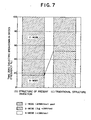
- a C-mode non-defective ratio of a dielectric breakdown strength test in oxides under the same electric field strength with an increased passage time of 60 min. or longer for a range between 1,150°C and 1,080°C according to the present invention reached to a value of as high as 80 % or higher as the case (B) shown in FIG. 7 and such a non-defective ratio was greatly higher in contrast with a ratio in the traditional case (C) shown in FIG. 7, in which a C-mode non-defective ratio fell in a range of 40 % to 60 %.
- the inventors of the present invention estimated temperatures in the bulk of a growing crystal in a variety of furnace structures by the numeral analysis method and devised a furnace structure suitable for limiting a gradual cooling process to the temperature range according to the present invention from the results thus obtained by the analysis method.
- a furnace structure is, as shown in FIG. 5 (b), to extend a hollow heat insulating cylinder 5 surrounding a heater 4 upward and place a carbon ring 7 on the upper end of the heat insulating cylinder 5.
- the extension of the heat insulating cylinder 5 and carbon ring 7 are not present in a traditional furnace structure ( FIG. 5 (a) ).
- the heat insulating cylinder 5 has an annular gap 8 for thermal separation in the mid portion between the upper part and lower part to successfully limit a rapid cooling process to a higher temperature range only.
- the annular separation gap 8 functions so as to increase a radiation loss from the growing crystal surface passing the vicinity of the gap 8.
- a vertical position of the gap 8 is important by the reason above mentioned and it is necessary to locate the gap 8 at a position at least higher than the height of the melt surface.
- a variety of analyses were done in regard to a width of the opening of the annular gap 8 and the results were such that the maximal width should be 10 cm because the effect of a gradual cooling in a temperature range of 1,150°C to 1,080°C was lost if a width of the gap was very large.
- FIGS. 6 (a) and 6 (b) A temperature profile along the length of a growing crystal in such a furnace structure was measured and the results were, as shown in FIGS. 6 (a) and 6 (b), that a passage time in a higher temperature range was made shorter and a passage time in a temperature range between 1,150°C and 1,080°C was made longer compared with that in a traditional furnace structure.
- FIG. 6 (b) a time required for growing crystal to pass a temperature difference of 50°C is plotted on an ordinate as a function of a temperature of the growing crystal on an abscissa.
- the present invention it becomes possible to decrease an absolute density of crystal defect nuclei, since a passage time for a growing crystal in a temperature range between 1,150°C and 1,080°C gets about 1.6 times as long as that in a traditional furnace structure and thereby a point defect is annihilated.
- a temperature gradient in a higher temperature range in the vicinity of the melting point which gradient does not affect the magnitude of a point defect density, can be made steep, a silicon crystal with a low defect density can be grown at a growth rate by about 10 % higher than that in a traditional furnace structure.
Landscapes
- Chemical & Material Sciences (AREA)
- Engineering & Computer Science (AREA)
- Crystallography & Structural Chemistry (AREA)
- Materials Engineering (AREA)
- Metallurgy (AREA)
- Organic Chemistry (AREA)
- Crystals, And After-Treatments Of Crystals (AREA)
- Liquid Deposition Of Substances Of Which Semiconductor Devices Are Composed (AREA)
Applications Claiming Priority (3)
| Application Number | Priority Date | Filing Date | Title |
|---|---|---|---|
| JP14339195 | 1995-06-09 | ||
| JP143391/95 | 1995-06-09 | ||
| JP7143391A JPH08337490A (ja) | 1995-06-09 | 1995-06-09 | 結晶欠陥の少ないシリコン単結晶及びその製造方法 |
Publications (3)
| Publication Number | Publication Date |
|---|---|
| EP0747513A2 true EP0747513A2 (fr) | 1996-12-11 |
| EP0747513A3 EP0747513A3 (fr) | 1997-05-28 |
| EP0747513B1 EP0747513B1 (fr) | 1999-09-15 |
Family
ID=15337683
Family Applications (1)
| Application Number | Title | Priority Date | Filing Date |
|---|---|---|---|
| EP96303989A Expired - Lifetime EP0747513B1 (fr) | 1995-06-09 | 1996-06-03 | Procede pour preparation d'un monocristal de silicium presentant une faible densite de defauts |
Country Status (5)
| Country | Link |
|---|---|
| US (1) | US5728211A (fr) |
| EP (1) | EP0747513B1 (fr) |
| JP (1) | JPH08337490A (fr) |
| KR (1) | KR100225274B1 (fr) |
| DE (1) | DE69604235T2 (fr) |
Cited By (13)
| Publication number | Priority date | Publication date | Assignee | Title |
|---|---|---|---|---|
| EP0875607A4 (fr) * | 1996-01-19 | 1999-04-14 | Shinetsu Handotai Kk | Monocristal de silicium, sans defaut du cristal dans la partie peripherique de la tranche, et procede pour produire ce monocristal |
| EP0909840A1 (fr) * | 1997-10-17 | 1999-04-21 | Shin-Etsu Handotai Company Limited | Procédé pour préparer un monocristal de silicium avec peu de défauts cristallins et le monocristal de silicium et plaquettes de silicium ainsi obtenus |
| EP0962557A1 (fr) * | 1998-06-03 | 1999-12-08 | Shin-Etsu Handotai Company Limited | Plaquette de silicium monocristallin et méthode pour sa production |
| WO2000022196A1 (fr) * | 1998-10-14 | 2000-04-20 | Memc Electronic Materials, Inc. | Procede de preparation de cristaux de silicium exempts de defauts permettant une certaine variabilite des conditions de traitement |
| US6312516B2 (en) | 1998-10-14 | 2001-11-06 | Memc Electronic Materials, Inc. | Process for preparing defect free silicon crystals which allows for variability in process conditions |
| US6328795B2 (en) | 1998-06-26 | 2001-12-11 | Memc Electronic Materials, Inc. | Process for growth of defect free silicon crystals of arbitrarily large diameters |
| US6409826B2 (en) | 1997-04-09 | 2002-06-25 | Memc Electronic Materials, Inc. | Low defect density, self-interstitial dominated silicon |
| US6416836B1 (en) | 1998-10-14 | 2002-07-09 | Memc Electronic Materials, Inc. | Thermally annealed, low defect density single crystal silicon |
| US6565649B2 (en) | 1998-10-14 | 2003-05-20 | Memc Electronic Materials, Inc. | Epitaxial wafer substantially free of grown-in defects |
| US6835245B2 (en) * | 2000-06-22 | 2004-12-28 | Sumitomo Mitsubishi Silicon Corporation | Method of manufacturing epitaxial wafer and method of producing single crystal as material therefor |
| US6858307B2 (en) | 2000-11-03 | 2005-02-22 | Memc Electronic Materials, Inc. | Method for the production of low defect density silicon |
| US7105050B2 (en) | 2000-11-03 | 2006-09-12 | Memc Electronic Materials, Inc. | Method for the production of low defect density silicon |
| US8216362B2 (en) | 2006-05-19 | 2012-07-10 | Memc Electronic Materials, Inc. | Controlling agglomerated point defect and oxygen cluster formation induced by the lateral surface of a silicon single crystal during CZ growth |
Families Citing this family (15)
| Publication number | Priority date | Publication date | Assignee | Title |
|---|---|---|---|---|
| JPH10152395A (ja) * | 1996-11-21 | 1998-06-09 | Komatsu Electron Metals Co Ltd | シリコン単結晶の製造方法 |
| US6379642B1 (en) * | 1997-04-09 | 2002-04-30 | Memc Electronic Materials, Inc. | Vacancy dominated, defect-free silicon |
| MY135749A (en) * | 1997-04-09 | 2008-06-30 | Memc Electronic Materials | Process for producing low defect density, ideal oxygen precipitating silicon |
| KR100395181B1 (ko) * | 1997-08-26 | 2003-08-21 | 미츠비시 스미토모 실리콘 주식회사 | 고품질 실리콘 단결정 및 그 제조방법 |
| KR100581305B1 (ko) | 1998-09-02 | 2006-05-22 | 엠이엠씨 일렉트로닉 머티리얼즈 인코포레이티드 | 저결함 밀도 단결정 실리콘으로부터의 soi 구조체 |
| JP2000154070A (ja) * | 1998-11-16 | 2000-06-06 | Suminoe Textile Co Ltd | セラミックス三次元構造体及びその製造方法 |
| JP4293395B2 (ja) | 1999-04-28 | 2009-07-08 | Sumco Techxiv株式会社 | Cz法単結晶インゴット製造装置及び方法 |
| US6635587B1 (en) | 1999-09-23 | 2003-10-21 | Memc Electronic Materials, Inc. | Method for producing czochralski silicon free of agglomerated self-interstitial defects |
| KR100745311B1 (ko) * | 1999-09-23 | 2007-08-01 | 엠이엠씨 일렉트로닉 머티리얼즈 인코포레이티드 | 냉각 속도를 제어함으로써 단결정 실리콘을 성장시키는초크랄스키 방법 |
| US6391662B1 (en) | 1999-09-23 | 2002-05-21 | Memc Electronic Materials, Inc. | Process for detecting agglomerated intrinsic point defects by metal decoration |
| JP4718668B2 (ja) * | 2000-06-26 | 2011-07-06 | 株式会社Sumco | エピタキシャルウェーハの製造方法 |
| KR100801672B1 (ko) | 2000-06-30 | 2008-02-11 | 신에쯔 한도타이 가부시키가이샤 | 실리콘 단결정 웨이퍼 및 그 제조방법 |
| US6846539B2 (en) * | 2001-01-26 | 2005-01-25 | Memc Electronic Materials, Inc. | Low defect density silicon having a vacancy-dominated core substantially free of oxidation induced stacking faults |
| TW200428637A (en) * | 2003-01-23 | 2004-12-16 | Shinetsu Handotai Kk | SOI wafer and production method thereof |
| JP6135818B2 (ja) * | 2014-02-24 | 2017-05-31 | 信越半導体株式会社 | シリコン単結晶製造方法 |
Family Cites Families (10)
| Publication number | Priority date | Publication date | Assignee | Title |
|---|---|---|---|---|
| DD258427A1 (de) * | 1987-03-16 | 1988-07-20 | Freiberg Spurenmetalle Veb | Verfahren und anordnung zur ueberwachung und regelung von kristallzuechtungsprozessen |
| JPH0259489A (ja) * | 1988-08-25 | 1990-02-28 | Shin Etsu Handotai Co Ltd | 化合物半導体単結晶の製造方法 |
| JPH0633235B2 (ja) * | 1989-04-05 | 1994-05-02 | 新日本製鐵株式会社 | 酸化膜耐圧特性の優れたシリコン単結晶及びその製造方法 |
| JPH0777995B2 (ja) * | 1989-11-16 | 1995-08-23 | 信越半導体株式会社 | 単結晶の比抵抗コントロール方法 |
| JP2686460B2 (ja) * | 1990-03-12 | 1997-12-08 | 住友シチックス株式会社 | 単結晶製造方法 |
| JPH06103714B2 (ja) * | 1990-11-22 | 1994-12-14 | 信越半導体株式会社 | シリコン単結晶の電気特性検査方法 |
| JP3016897B2 (ja) * | 1991-03-20 | 2000-03-06 | 信越半導体株式会社 | シリコン単結晶の製造方法及び装置 |
| DE4301072B4 (de) * | 1993-01-16 | 2006-08-24 | Crystal Growing Systems Gmbh | Verfahren zum Ziehen von Einkristallen aus einer Schmelze |
| JPH0761889A (ja) * | 1993-08-26 | 1995-03-07 | Komatsu Electron Metals Co Ltd | 半導体単結晶引き上げ装置および引き上げ方法 |
| JP3285111B2 (ja) * | 1994-12-05 | 2002-05-27 | 信越半導体株式会社 | 結晶欠陥の少ないシリコン単結晶の製造方法 |
-
1995
- 1995-06-09 JP JP7143391A patent/JPH08337490A/ja active Pending
-
1996
- 1996-06-03 US US08/660,198 patent/US5728211A/en not_active Expired - Fee Related
- 1996-06-03 EP EP96303989A patent/EP0747513B1/fr not_active Expired - Lifetime
- 1996-06-03 DE DE69604235T patent/DE69604235T2/de not_active Expired - Fee Related
- 1996-06-05 KR KR1019960019997A patent/KR100225274B1/ko not_active Expired - Fee Related
Cited By (25)
| Publication number | Priority date | Publication date | Assignee | Title |
|---|---|---|---|---|
| EP0875607A4 (fr) * | 1996-01-19 | 1999-04-14 | Shinetsu Handotai Kk | Monocristal de silicium, sans defaut du cristal dans la partie peripherique de la tranche, et procede pour produire ce monocristal |
| US6120749A (en) * | 1996-01-19 | 2000-09-19 | Shin-Etsu Handotai Co., Ltd | Silicon single crystal with no crystal defect in peripheral part of wafer and process for producing the same |
| US6632278B2 (en) | 1997-04-09 | 2003-10-14 | Memc Electronic Materials, Inc. | Low defect density epitaxial wafer and a process for the preparation thereof |
| US6409826B2 (en) | 1997-04-09 | 2002-06-25 | Memc Electronic Materials, Inc. | Low defect density, self-interstitial dominated silicon |
| EP0909840A1 (fr) * | 1997-10-17 | 1999-04-21 | Shin-Etsu Handotai Company Limited | Procédé pour préparer un monocristal de silicium avec peu de défauts cristallins et le monocristal de silicium et plaquettes de silicium ainsi obtenus |
| US6027562A (en) * | 1997-10-17 | 2000-02-22 | Shin-Etsu Handotai Co., Ltd | Method for producing a silicon single crystal having few crystal defects, and a silicon single crystal and silicon wafers produced by the method |
| US6120598A (en) * | 1997-10-17 | 2000-09-19 | Shin-Etsu Handotai Co., Ltd. | Method for producing a silicon single crystal having few crystal defects, and a silicon single crystal and silicon wafers produced by the method |
| EP0962557A1 (fr) * | 1998-06-03 | 1999-12-08 | Shin-Etsu Handotai Company Limited | Plaquette de silicium monocristallin et méthode pour sa production |
| US6299982B1 (en) | 1998-06-03 | 2001-10-09 | Shin-Etsu Handotai Co., Ltd. | Silicon single crystal wafer and method for producing silicon single crystal wafer |
| US6913647B2 (en) | 1998-06-26 | 2005-07-05 | Memc Electronic Materials, Inc. | Process for cooling a silicon ingot having a vacancy dominated region to produce defect free silicon |
| US6328795B2 (en) | 1998-06-26 | 2001-12-11 | Memc Electronic Materials, Inc. | Process for growth of defect free silicon crystals of arbitrarily large diameters |
| US6562123B2 (en) | 1998-06-26 | 2003-05-13 | Memc Electronic Materials, Inc. | Process for growing defect-free silicon wherein the grown silicon is cooled in a separate chamber |
| US6500255B2 (en) | 1998-10-14 | 2002-12-31 | Memc Electronic Materials, Inc. | Process for growing silicon crystals which allows for variability in the process conditions while suppressing the formation of agglomerated intrinsic point defects |
| US6416836B1 (en) | 1998-10-14 | 2002-07-09 | Memc Electronic Materials, Inc. | Thermally annealed, low defect density single crystal silicon |
| US6565649B2 (en) | 1998-10-14 | 2003-05-20 | Memc Electronic Materials, Inc. | Epitaxial wafer substantially free of grown-in defects |
| US6312516B2 (en) | 1998-10-14 | 2001-11-06 | Memc Electronic Materials, Inc. | Process for preparing defect free silicon crystals which allows for variability in process conditions |
| US6652646B2 (en) | 1998-10-14 | 2003-11-25 | Memc Electronic Materials, Inc. | Process for growing a silicon crystal segment substantially free from agglomerated intrinsic point defects which allows for variability in the process conditions |
| US6743289B2 (en) | 1998-10-14 | 2004-06-01 | Memc Electronic Materials, Inc. | Thermal annealing process for producing low defect density single crystal silicon |
| WO2000022196A1 (fr) * | 1998-10-14 | 2000-04-20 | Memc Electronic Materials, Inc. | Procede de preparation de cristaux de silicium exempts de defauts permettant une certaine variabilite des conditions de traitement |
| US7097718B2 (en) | 1998-10-14 | 2006-08-29 | Memc Electronic Materials, Inc. | Single crystal silicon wafer having an epitaxial layer substantially free from grown-in defects |
| US6835245B2 (en) * | 2000-06-22 | 2004-12-28 | Sumitomo Mitsubishi Silicon Corporation | Method of manufacturing epitaxial wafer and method of producing single crystal as material therefor |
| US6858307B2 (en) | 2000-11-03 | 2005-02-22 | Memc Electronic Materials, Inc. | Method for the production of low defect density silicon |
| US7105050B2 (en) | 2000-11-03 | 2006-09-12 | Memc Electronic Materials, Inc. | Method for the production of low defect density silicon |
| US8216362B2 (en) | 2006-05-19 | 2012-07-10 | Memc Electronic Materials, Inc. | Controlling agglomerated point defect and oxygen cluster formation induced by the lateral surface of a silicon single crystal during CZ growth |
| US8673248B2 (en) | 2006-05-19 | 2014-03-18 | Memc Electronic Materials, Inc. | Silicon material with controlled agglomerated point defects and oxygen clusters induced by the lateral surface |
Also Published As
| Publication number | Publication date |
|---|---|
| EP0747513A3 (fr) | 1997-05-28 |
| US5728211A (en) | 1998-03-17 |
| DE69604235T2 (de) | 2000-03-16 |
| EP0747513B1 (fr) | 1999-09-15 |
| JPH08337490A (ja) | 1996-12-24 |
| DE69604235D1 (de) | 1999-10-21 |
| KR100225274B1 (ko) | 1999-10-15 |
Similar Documents
| Publication | Publication Date | Title |
|---|---|---|
| EP0747513A2 (fr) | Monocristal de silicium présentant une faible densité de défauts et procédé pour sa préparation | |
| EP1270769B1 (fr) | Procede de production d'un monocristal de silicium sans defaut | |
| KR100582240B1 (ko) | 실리콘 단결정 웨이퍼 및 그 제조방법 | |
| EP0890662B1 (fr) | Methode et procédé de production d'un monocristal de silicium a defauts cristallins reduits et le monocristal et plaquette de silicium ainsi obtenus | |
| EP0962555B1 (fr) | Procédé pour la préparation d'un monocristal | |
| US8382894B2 (en) | Process for the preparation of silicon wafer with reduced slip and warpage | |
| KR100453850B1 (ko) | 웨이퍼주변부에결정결함이없는실리콘단결정 | |
| DE112013001054B4 (de) | Verfahren zum Herstellen eines Silizium-Einkristall-Wafers | |
| KR100710700B1 (ko) | 실리콘 단결정의 제조 방법, 단결정 잉곳 제조 장치 및실리콘 단결정 웨이퍼의 열처리 방법 | |
| EP0942077B1 (fr) | Procédé pour la production d'une plaquette de silicium monocristallin et plaquette de silicium monocristallin ainsi obtenue | |
| KR20050052478A (ko) | 어닐 웨이퍼 및 어닐 웨이퍼의 제조방법 | |
| US5137847A (en) | Method of producing GaAs single crystal substrate using three stage annealing and interstage etching | |
| KR100932742B1 (ko) | 실리콘 단결정 웨이퍼와 에피텍셜 웨이퍼 및 실리콘 단결정의 제조방법 | |
| KR20000006142A (ko) | 질소도프된저결함실리콘단결정의제조방법 | |
| US7204881B2 (en) | Silicon wafer for epitaxial growth, an epitaxial wafer, and a method for producing it | |
| EP1804283B1 (fr) | Procédé de fabrication d'une plaquette recuite | |
| US6709957B2 (en) | Method of producing epitaxial wafers | |
| KR19980070037A (ko) | 반도체 잉곳 성장시 시드결정의 인상속도 최적화방법, 이를 적용한 반도체 잉곳 성장방법, 그에 따라 성장된 반도체 잉곳과반도체 웨이퍼 및 반도체장치 | |
| US6544332B1 (en) | Method for manufacturing silicon single crystal, silicon single crystal manufactured by the method, and silicon wafer | |
| KR20020060244A (ko) | 어닐 웨이퍼의 제조방법 및 어닐 웨이퍼 | |
| JP2503697B2 (ja) | 半絶縁性GaAs単結晶の製造方法 | |
| US6461447B1 (en) | Substrate for epitaxial growth | |
| JP2003321297A (ja) | シリコン単結晶の製造方法及びシリコン単結晶ウェーハ | |
| CN119082865A (zh) | 硅片及硅片的形成方法 | |
| KR20010101046A (ko) | 실리콘 단결정 및 실리콘 단결정 웨이퍼의 제조 방법 |
Legal Events
| Date | Code | Title | Description |
|---|---|---|---|
| PUAI | Public reference made under article 153(3) epc to a published international application that has entered the european phase |
Free format text: ORIGINAL CODE: 0009012 |
|
| AK | Designated contracting states |
Kind code of ref document: A2 Designated state(s): DE FR GB |
|
| PUAL | Search report despatched |
Free format text: ORIGINAL CODE: 0009013 |
|
| AK | Designated contracting states |
Kind code of ref document: A3 Designated state(s): DE FR GB |
|
| 17P | Request for examination filed |
Effective date: 19970426 |
|
| 17Q | First examination report despatched |
Effective date: 19970630 |
|
| GRAG | Despatch of communication of intention to grant |
Free format text: ORIGINAL CODE: EPIDOS AGRA |
|
| GRAG | Despatch of communication of intention to grant |
Free format text: ORIGINAL CODE: EPIDOS AGRA |
|
| GRAG | Despatch of communication of intention to grant |
Free format text: ORIGINAL CODE: EPIDOS AGRA |
|
| GRAH | Despatch of communication of intention to grant a patent |
Free format text: ORIGINAL CODE: EPIDOS IGRA |
|
| GRAH | Despatch of communication of intention to grant a patent |
Free format text: ORIGINAL CODE: EPIDOS IGRA |
|
| GRAA | (expected) grant |
Free format text: ORIGINAL CODE: 0009210 |
|
| AK | Designated contracting states |
Kind code of ref document: B1 Designated state(s): DE FR GB |
|
| PG25 | Lapsed in a contracting state [announced via postgrant information from national office to epo] |
Ref country code: FR Free format text: LAPSE BECAUSE OF FAILURE TO SUBMIT A TRANSLATION OF THE DESCRIPTION OR TO PAY THE FEE WITHIN THE PRESCRIBED TIME-LIMIT Effective date: 19990915 |
|
| REF | Corresponds to: |
Ref document number: 69604235 Country of ref document: DE Date of ref document: 19991021 |
|
| EN | Fr: translation not filed | ||
| PG25 | Lapsed in a contracting state [announced via postgrant information from national office to epo] |
Ref country code: GB Free format text: LAPSE BECAUSE OF NON-PAYMENT OF DUE FEES Effective date: 20000603 |
|
| PLBE | No opposition filed within time limit |
Free format text: ORIGINAL CODE: 0009261 |
|
| STAA | Information on the status of an ep patent application or granted ep patent |
Free format text: STATUS: NO OPPOSITION FILED WITHIN TIME LIMIT |
|
| 26N | No opposition filed | ||
| GBPC | Gb: european patent ceased through non-payment of renewal fee |
Effective date: 20000603 |
|
| PGFP | Annual fee paid to national office [announced via postgrant information from national office to epo] |
Ref country code: DE Payment date: 20020612 Year of fee payment: 7 |
|
| PG25 | Lapsed in a contracting state [announced via postgrant information from national office to epo] |
Ref country code: DE Free format text: LAPSE BECAUSE OF NON-PAYMENT OF DUE FEES Effective date: 20040101 |