EP0747970A2 - Vorrichtung und Verfahren für die Ableitung einer Restladung in einem Bildaufnahmesystem - Google Patents
Vorrichtung und Verfahren für die Ableitung einer Restladung in einem Bildaufnahmesystem Download PDFInfo
- Publication number
- EP0747970A2 EP0747970A2 EP96107889A EP96107889A EP0747970A2 EP 0747970 A2 EP0747970 A2 EP 0747970A2 EP 96107889 A EP96107889 A EP 96107889A EP 96107889 A EP96107889 A EP 96107889A EP 0747970 A2 EP0747970 A2 EP 0747970A2
- Authority
- EP
- European Patent Office
- Prior art keywords
- radiation
- image capture
- panel
- layer
- sensitive layer
- Prior art date
- Legal status (The legal status is an assumption and is not a legal conclusion. Google has not performed a legal analysis and makes no representation as to the accuracy of the status listed.)
- Granted
Links
Images

Classifications
-
- G—PHYSICS
- G01—MEASURING; TESTING
- G01T—MEASUREMENT OF NUCLEAR OR X-RADIATION
- G01T1/00—Measuring X-radiation, gamma radiation, corpuscular radiation, or cosmic radiation
- G01T1/16—Measuring radiation intensity
- G01T1/24—Measuring radiation intensity with semiconductor detectors
-
- H—ELECTRICITY
- H04—ELECTRIC COMMUNICATION TECHNIQUE
- H04N—PICTORIAL COMMUNICATION, e.g. TELEVISION
- H04N23/00—Cameras or camera modules comprising electronic image sensors; Control thereof
- H04N23/30—Cameras or camera modules comprising electronic image sensors; Control thereof for generating image signals from X-rays
-
- H—ELECTRICITY
- H04—ELECTRIC COMMUNICATION TECHNIQUE
- H04N—PICTORIAL COMMUNICATION, e.g. TELEVISION
- H04N25/00—Circuitry of solid-state image sensors [SSIS]; Control thereof
- H04N25/60—Noise processing, e.g. detecting, correcting, reducing or removing noise
- H04N25/62—Detection or reduction of noise due to excess charges produced by the exposure, e.g. smear, blooming, ghost image, crosstalk or leakage between pixels
- H04N25/626—Reduction of noise due to residual charges remaining after image readout, e.g. to remove ghost images or afterimages
-
- H—ELECTRICITY
- H04—ELECTRIC COMMUNICATION TECHNIQUE
- H04N—PICTORIAL COMMUNICATION, e.g. TELEVISION
- H04N25/00—Circuitry of solid-state image sensors [SSIS]; Control thereof
- H04N25/70—SSIS architectures; Circuits associated therewith
- H04N25/76—Addressed sensors, e.g. MOS or CMOS sensors
Definitions
- the present invention pertains to an image capture panel for capturing direct radiographic images. More particularly, the present invention pertains to a method and apparatus for eliminating residual electrical charges residing in the image capture panel prior to capture of a subsequent radiographic image.
- Radiograms have also been produced by using layers of radiation sensitive materials to directly capture radiographic images as imagewise modulated patterns of electrical charges.
- electrical charges generated either electrically or optically by the X-ray radiation within a pixelized area are quantized using a regularly arranged array of discrete solid state radiation sensors.
- U. S. Patent No. 5,319,206 issued to Lee et al. on June 7, 1994 and assigned to E. I. du Pont de Nemours and Company, describes a system employing a layer of photoconductive material to create an imagewise modulated areal distribution of electron-hole pairs which are subsequently converted to corresponding analog pixel (picture element) values by electrosensitive devices, such as thin-film transistors.
- 5,262,649 (Antonuk et al.) describes a system employing a layer of phosphor or scintillation material to create an imagewise modulated distribution of photons which are subsequently converted to a corresponding image-wise modulated distribution of electrical charges by photosensitive devices, such as amorphous silicon photodiodes.
- U. S. Patent No. 5,254,480 (Tran) describes a system which combines a luminescent layer, to create a distribution of photons, with an adjacent layer of photoconductive material to create a corresponding image-wise modulated distribution of electrical charges which are subsequently converted to corresponding analog pixel values for the image by electrosensitive devices.
- These solid state systems have the advantage of being useful for repeated exposures to X-ray radiation without consumption and chemical processing of silver halide films.
- the top areal surface of the photoconductive layer is uniformly biased relative to electrical charge read-out means by application of an appropriate electric field.
- electron-hole pairs are generated in the photoconductive layer in response to the intensity of the imagewise modulated pattern of X-ray radiation, and these electron-hole pairs are separated by the applied biasing electric field.
- the electron-hole pairs move in opposite directions along the electric field lines toward opposing surfaces of the photoconductive layer.
- a latent image in the form of an imagewise distribution of electrical charges of varying magnitude is captured within the photoconductive layer, representing a latent electrostatic radiogram.
- a plurality of charge capture elements and switching devices proximate the photoconductive layer are adapted to readout the imagewise distribution of electrical charges, thereby providing a pixelized radiogram.
- a problem with such an electrical charge capture and readout scheme is that after exposure to X-ray radiation is stopped and the electronic charge distribution within the photoconductive layer is determined by readout, some of the electrical charges induced within the photoconductive layer may continue to reside as charges trapped not only within the photoconductive layer but also at planar interfaces between the surfaces of the photoconductive layer and adjacent layers. These residual electrical charges must be fully eliminated prior to the next X-ray exposure. Otherwise, a false image pattern related to the previous radiation pattern may be added to subsequent radiograms.
- Residual charges have also been minimized by application of a reversed and decreasing electric field, for example, as described in U.S. Patent No. 5,319,206.
- this process involves multiple applications of a decreasing and reversed electric field to fully neutralize residual electrical charges remaining in the photoconductive layer.
- the present invention provides an apparatus and method for eliminating residual charges in an image capture panel that includes a plurality of sensors arrayed adjacent to a substrate layer of dielectric material.
- a radiation sensitive layer is disposed over the sensors.
- the radiation sensitive layer is exposed to a first substantially uniform pattern of light radiation for partially neutralizing residual electrical charges trapped within the image capture panel.
- the radiation sensitive layer is then exposed to a second substantially uniform pattern of light radiation sufficient to neutralize substantially all residual electrical charges trapped within the image capture panel.
- Figure 1 is a schematic cross-sectional view of an X-ray image capture element illustrating the present invention.
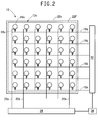
- Figure 2 is a schematic top view of the X-ray image capture element shown in Figure 1.
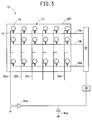
- Figure 3 is another schematic top view of the X-ray image capture element shown in Figure 1.
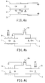
- Figures 4a, 4b and 4c are schematic views illustrating the present method.
- FIG. 1 shows an X-ray image capture panel 10 for capturing an imagewise modulated pattern of incident radiation. Radiation is herein meant to include high energy electromagnetic waves, especially X-rays with energy levels between about 20 Kev and about 150 Kev.
- the image capture panel 10 comprises a dielectric substrate layer 7 having a top and bottom surface.
- a plurality of radiation sensitive sensors 12n i.e., 12a, 12b, 12c, ..., 12n
- the sensors 12n are read out by suitable electrical readout means 5n.
- the readout means 5n typically comprises means for electronically accessing each of the sensors 12n individually, and means for individually determining electric charge captured in the sensors 12n.
- the sensors 12n comprise a plurality of switching devices 14n (i.e., 14a, 14b, 14c, ..., 14n) and a plurality of sensing elements 16n (i.e., 16a, 16b, 16c, ..., 16n).
- the sensing elements 16n comprise a first plurality of conductive microplates 24n (i.e., 24a, 24b, 24c, ..., 24n) deposited on the substrate layer 7 and covered with a capacitive dielectric material 15, for example, silicon dioxide.
- a second plurality of conductive microplates 26 n i.e., 26a, 26b, 26c, ..., 26n
- the substrate layer 7 preferably comprises a material substantially transparent to light, for example, glass.
- the conductive microplates 24n and 26n have a low optical density, for example, a thin layer of indium-tin-oxide (ITO) or a thin layer between 50 and 100 ⁇ of metal, such as gold or aluminum.
- ITO indium-tin-oxide
- FIG. 1 shows the sensing elements 16n which function as charge storage capacitors formed by the microplates 26n, the microplates 24n and the capacitive dielectric material 15.
- Each microplate 26n is connected to the adjacent switching device 14n.
- the switching devices 14n are preferably thin-film field effect transistors (FETs) comprising a layer 13 of hydrogenated amorphous-silicon, crystalline silicon, polycrystalline silicon or cadmium selenide, an insulating layer 99, a conductive gate 21 and two conductive electrodes 23 and 25.
- FETs thin-film field effect transistors
- Each electrode 23 is connected to one of a plurality of readout lines 20n (shown in Figure 2) and acts as a drain electrode.
- Each electrode 25 is connected to one of the microplates 26n and acts as a source electrode.
- Each switching device 14n has its gate 21 connected to a switching line 18n (shown in Figure 2), and serves as a bi-directional switch allowing current flow between the readout line 20n and the sensing element 16n depending on whether a bias voltage is applied to the gate 21 through the switching line 18n.
- Each switching device 14n is covered with a passivation layer 98.
- the passivation layer 98 has a thickness greater than that of the insulating layer 99.
- the sensing elements 16n further comprise a plurality of conductive collecting elements 6n (i.e., 6a, 6b, 6c, ..., 6n) deposited, respectively, over the microplates 26n and over the switching devices 14n.
- a charge blocking layer 28 Over the top surface of the collecting elements 6n is disposed a charge blocking layer 28 having a thickness selected to prevent charge leakage. Both the conductive collecting elements 6n and the charge blocking layer 28 also have a low optical density.
- the charge blocking layer 28 is preferably provided by an aluminum oxide layer formed on the collecting elements 6n although other blocking interfaces may also be used.
- FIG. 2 shows a plurality of conductive switching lines 18n and conductive readout lines 20n disposed in the spaces between the sensors 12n.
- the switching devices 14n are disposed in the spaces between the sensing elements 16n, the switching lines 18n, and the readout lines 20n.
- the switching lines 18n are individually accessible through a plurality of leads connected to a multiplexing device 32.
- each switching device 14n serves as a bi-directional switch allowing current flow between the readout line 20n and the sensing element 16n depending on whether a bias voltage is applied to the gate 21 through the switching line 18n.
- Figure 1 further shows a radiation sensitive layer 8, preferably a layer of photoconductive material, disposed over the charge blocking layer 28, the switching lines 18n and the readout lines 20n.
- the combination of layers 6n, 28 and 8 behaves as a blocking diode, inhibiting one type of charge flow in one direction.
- the photoconductive layer 8 preferably exhibits very high dark resistivity and may comprise amorphous selenium, lead oxide, thallium bromide, cadmium telluride, cadmium sulfide, mercuric iodide or any other such material.
- the photoconductive layer 8 may also comprise organic materials such as photoconductive polymers loaded with X-ray absorbing compounds, which exhibit photoconductivity.
- the photoconductive layer 8 comprises 300 to 500 micrometers of amorphous selenium in order to provide high efficiency in X-ray radiation detection, and the charge blocking layer 28 has a thickness greater than 100 ⁇ .
- a top dielectric layer 11 having a thickness greater than one micrometer is disposed over the top surface of the photoconductive layer 8.
- Mylar® (i.e., polyethylene terephthalate) film with a thickness of 25 micrometers may be laminated for the dielectric layer 11 or, preferably, a dielectric material such as Parylene® (i.e., poly-xylylene) may be vacuum deposited to form the dielectric layer 11.
- Parylene® i.e., poly-xylylene
- ITO indium-tin-oxide
- metal like chromium being essentially transparent to light
- the entire image capture panel 10 can be made by depositing sensors 12n, blocking layer 28, photoconductive layer 8, top dielectric layer 11, and top conductive layer 9 upon the dielectric substrate layer 7. Fabrication may be accomplished, for example, by plasma-enhanced chemical vapor deposition, vacuum deposition, lamination, or sputtering.
- Figure 1 shows light exposure means L juxtaposed the image capture panel 10. It has been discovered that the light exposure means L is effective in eliminating residual electrical charges that may reside within the image capture panel 10 and create a false image in a subsequent imagewise radiation operation.
- the light exposure means L is positioned to provide a uniform pattern of low energy light radiation over the photoconductive layer 8.
- the light exposure means L comprises a first light emitting panel 22F positioned above and displaced a small distance, for example 2 millimeters, from the top conductive layer 9.
- the first panel 22F is adapted to expose the photoconductive layer 8 to a first pattern of low energy light radiation.
- the term "light” is used herein to describe low energy electromagnetic radiation having wavelengths in the range 400 to 800 nanometers with energy in the range 20 to 1000 erg/cm 2 .
- This first pattern of low energy light radiation is selected to have wavelengths and energy such that the light is capable of penetrating the top conductive layer 9 and top dielectric layer 11 with minimal absorption but being essentially totally absorbed near the top portion of the photoconductive layer 8.
- the light emitting panel 22F is a panel woven from plastic strands of optic fibers, like that available from Lumitex, Inc., Strongsville, OH.
- the panel 22F should be capable of providing a substantially uniform pattern of low energy light radiation, have a broad range of wavelengths in the 400 to 800 nanometers range, and provide energy per unit area in the range from 20 to 1000 erg/cm 2 , preferably about 500 erg/cm 2 . Since X-rays must penetrate the first panel 22F during patient exposure, it is necessary that the first panel 22F comprise material having both low X-ray attenuation and a uniform X-ray density. The uniform X-ray density is important in order to prevent any internal panel structure from appearing in the X-ray image.
- a remote source 22L of low energy light radiation preferably a tungsten-halogen source, is coupled to the light emitting panel 22F through polished fiber ends of the light emitting panel 22F in order to provide low energy light radiation into the light emitting panel 22F.
- Light transmitted into the optic fibers is emitted from the sides of the fibers, passes through the conductive layer 9 and the dielectric layer 11, and then onto the photoconductive layer 8.
- the selection of multiple layers of woven optic fibers allows more efficient use of the low energy light radiation source 22L, and enhances the brightness and uniformity of the low energy light radiation incident on the top conductive layer 9.
- the light exposure means L further comprises a second light emitting panel 22S positioned below the substrate 7 and displaced a small distance, for example 2 millimeters, from the substrate 7.
- the second panel 22S is adapted to provide a second pattern of low energy light radiation over the substrate 7 and therethrough onto the photoconductive layer 8.
- the light emitting panel 22S is an electroluminescent low energy light radiation panel, such as a panel commercially available from BKL, Inc., King of Prussia, PA, under the tradename "Aviation Green N3.”
- This panel 22S is composed of electroluminescent material sandwiched between thin foils of ITO and Al and is capable of providing a uniform pattern of low energy light radiation having wavelengths in the 400 to 800 nanometer range, and providing energy per unit area in the range from 20 to 1000 erg/cm 2 , preferably about 400 erg/cm 2 .
- the source of low energy light radiation is energy emission from the electroluminescent material in response to power provided to the light emitting panel 22S.
- the light emitting panel 22S is oriented so that the ITO-coated surface is adjacent to the image capture panel 10.
- This second pattern of low energy light radiation is selected to have wavelengths and energy such that the light is capable of penetrating the dielectric substrate 7, the microplates 24n and 26n, the collecting elements 6n and the charge blocking layer 28 with minimal absorption but being essentially totally absorbed near the bottom portion of the photoconductive layer 8.
- the first light emitting panel 22F is co-extensive with the array of sensors 12n.
- the second light emitting panel 22S is shown in dashed lines and is also co-extensive with the array of sensors 12n.
- an imagewise modulated pattern of X-ray radiation is incident upon the image capture panel 10 which is positioned proximate the patient.
- electrical charges residual in the image capture panel 10 are minimized in order to eliminate false or ghost image patterns.
- the operating bias voltage from the power supply 19P is reduced to zero, and all readout switch gates 21 are activated to bring the collecting elements 6n and the top conductive layer 9 to a common zero potential.
- the first light emitting panel 22F is activated to flash expose the photoconductive layer 8 to a first uniform pattern of low energy light radiation.
- This first flash exposure is adjusted in energy to create sufficient electrical charge carriers within the photoconductive layer 8 to partially neutralize residual electrical charges remaining within the bulk of the photoconductive layer 8 and remaining near the interface between the photoconductive layer 8 and the top dielectric layer 11.
- a light radiation flash exposure providing energy in the range from 20 to 1000 erg/cm 2 over a time interval of 1 to 30 seconds has proved adequate.
- This first creation of free electrical charges serves to partially eliminate any localized higher level accumulations of electrical charges trapped within the bulk of the photoconductive layer 8 and remaining near the interface between the photoconductive layer 8 and the sensors 12n prior to activation of the second light emitting panel 22S.
- the second light emitting panel 22S is next activated to flash expose the photoconductive layer 8 to a second uniform pattern of low energy light radiation.
- This second flash exposure is adjusted to have an energy output that produces an abundant supply of electron-hole pairs within the photoconductive layer 8 sufficient to effectively neutralize or eliminate all residual electrical charges trapped either within the bulk of the photoconductive layer 8 or near the interface between the photoconductive layer 8 and the sensors 12n. By eliminating the residual electric charges, the electric field that exists across the dielectric layer 11 is eliminated.
- FIG. 3 shows the operation of the image capture panel 10 during image capture and readout.
- Each readout line 20n is connected to a readout means 34 comprising a charge integrating amplifier device 41n, and a sample-and-hold circuit 45n.
- the output of circuit 45n may be sampled sequentially to obtain an X-ray radiation image output signal, and the technology to do this is well known in the art. Additional electronic manipulations not related to the present invention may be performed before or after image capture to enhance the overall quality of the final radiation image.
- a patient to be examined is exposed to a uniform pattern of X-ray radiation producing an imagewise modulated pattern of X-ray radiation incident on the image capture panel 10. This pattern generates a corresponding imagewise modulated pattern of electrical charges in the array of sensing elements 16n.
- a microprocessor controller 38 causes the multiplexing device 32 to read out a pattern of electrical charge values corresponding to the pattern of X-ray radiation absorption in the patient.
- the panel 10 is cleared of any residual charges using the sequence of reducing the distribution in the amplitudes of residual electrical charges remaining near the surface 2 of the photoconductive layer 8 and, thereafter, fully eliminating all residual electric charges retained near the surface 3 of the layer 8, using the first and second exposure devices 22F and 22S, respectively, as described herein.
- This residual charge reduction process may be repeated if appropriate until all the trapped charges are removed and the image capture panel 10 is prepared for a subsequent image capture operation.
- both the first and the second patterns of light radiation may be provided from a single light emitting panel, e.g., the second light emitting panel 22F.
- the first light emitting panel 22F is cooperatively combined with the second light emitting panel 22S in order to eliminate all residual electrical charges without exceeding the current capabilities of the readout means 5.
- the first panel 22F is utilized to reduce the overall intensity of any remaining trapped electrical charges, while the second panel 22S serves to completely eliminate all remaining electrical charges.
- Figure 4a shows a simplified electrical description of this combination of intensity reduction of localized trapped electrical charges prior to elimination of all trapped electrical charges.
- the preferred process for neutralizing any residual charges remaining within the photoconductive layer 8 utilizes two sources of low energy light radiation 22F and 22S.
- the readout means 5 and the top conductive layer 9 are shorted to ground, and the operating bias voltage from the power supply 19P is reduced to zero, an uneven distribution of electrical charges may remain "trapped" within the photoconductive layer 8 because of the limited charge transport range of the "minority carrier" of the radiation induced electron-hole pair.
- These charges are trapped in the bulk of the photoconductive layer 8 as well as near the interface with the dielectric layer 11, and attract electric charges of the opposite polarity in the nearby grounded layers.
- the dielectric layer 11 and the radiation sensitive photoconductive layer 8 thus form two capacitors in series, designated as Cd and Crs, respectively, for each of the sensors 12n.
- the lower surface of the dielectric layer 11 is indicated by the character 1
- the juxtaposed surface of the photoconductive layer 8 is indicated by the character 2.
- the photoconductive layer 8 has positively charged holes as the "majority carrier", such as P type selenium
- the minority charge carriers created in the layer 8 by an incident imagewise modulated pattern of radiation will have a limited charge transport range and a corresponding shorter range within the bulk of the layer 8. Consequently, following a first radiation exposure and readout operation similar to that described above, trapped charges residual in the photoconductive layer 8, shown as "-" charges, will generally be non-uniformly distributed throughout the image capture panel 10.
- Figure 4b shows a simplified electrical equivalent circuit illustrative of the present invention wherein the first flash exposure, indicated by FR in Figure 4b, is incident through the top dielectric layer 11 and into the photoconductive layer 8.
- this first flash exposure is largely absorbed near the surface of the photoconductive layer 8 but is adjusted in energy to create sufficient electron-hole pairs within the photoconductive layer 8 to combine with residual trapped electrical charges and partially eliminate any electrical charges retained primarily near the surface 2 of the photoconductive layer 8. Because of the limited charge transport range of the minority charge carriers, only a limited number of the residual trapped electrical charges will be eliminated. However, by partially reducing the number of residual trapped electrical charges, the first flash exposure beneficially produces an overall reduced maximum amplitude of residual electric fields in Cd throughout the sensors 12n within the panel 10.
- FIG 4C shows a simplified electrical equivalent circuit illustrative of the present invention wherein the second flash exposure, indicated by SR in Figure 4c, is incident through the dielectric substrate 7 and through the plurality of sensors 12n.
- this second flash exposure is largely absorbed near the surface of the photoconductive layer 8 but is adjusted in energy to create sufficient electron-hole pairs within the photoconductive layer 8 to combine with the residual trapped electrical charges, thereby fully eliminating all residual electric charges retained within the panel 10.
- the second flash exposure SR may be performed by applying the second pattern at a rate in the range from 20 to 800 erg/cm2 per second.
- the second flash exposure rate is time-wise adjusted so that the incident radiation is applied at an increasing rate from 20 to 800 erg/cm 2 per second, thereby generating a slowly increasing number of electron-hole pairs while eliminating the residual electrical charges.
- This process of first reducing the distribution in the amplitudes of residual electrical charges remaining near the surface 2 of the photoconductive layer 8 and thereafter fully eliminating all residual electrical charges retained near the top conductive layer 9 is effective in protecting the readout means 5n within the panel 10 because the amplitudes of electric fields attributable to residual charges being discharged from the panel 10 through the readout means 5n are lowered.
- an N type radiation sensitive material such as cadmium selenide which has negatively charged electrons as the "majority carrier".
- the minority charge carriers which are created in the photoconductive layer 8 and have a limited charge transport range, are positively charged. The process described above is again effective in protecting the readout means 5n within the panel 10 although the operating bias voltage applied to the top conductive layer 9 is reversed.
Landscapes
- Engineering & Computer Science (AREA)
- Multimedia (AREA)
- Signal Processing (AREA)
- General Physics & Mathematics (AREA)
- Health & Medical Sciences (AREA)
- Life Sciences & Earth Sciences (AREA)
- Physics & Mathematics (AREA)
- High Energy & Nuclear Physics (AREA)
- Molecular Biology (AREA)
- Spectroscopy & Molecular Physics (AREA)
- Measurement Of Radiation (AREA)
- Solid State Image Pick-Up Elements (AREA)
- Transforming Light Signals Into Electric Signals (AREA)
- Apparatus For Radiation Diagnosis (AREA)
- Analysing Materials By The Use Of Radiation (AREA)
Applications Claiming Priority (2)
| Application Number | Priority Date | Filing Date | Title |
|---|---|---|---|
| US08/475,449 US5563421A (en) | 1995-06-07 | 1995-06-07 | Apparatus and method for eliminating residual charges in an image capture panel |
| US475449 | 1995-06-07 |
Publications (3)
| Publication Number | Publication Date |
|---|---|
| EP0747970A2 true EP0747970A2 (de) | 1996-12-11 |
| EP0747970A3 EP0747970A3 (de) | 1998-09-02 |
| EP0747970B1 EP0747970B1 (de) | 2004-12-15 |
Family
ID=23887607
Family Applications (1)
| Application Number | Title | Priority Date | Filing Date |
|---|---|---|---|
| EP96107889A Expired - Lifetime EP0747970B1 (de) | 1995-06-07 | 1996-05-17 | Vorrichtung für die Ableitung einer Restladung in einem Bildaufnahmesystem |
Country Status (5)
| Country | Link |
|---|---|
| US (1) | US5563421A (de) |
| EP (1) | EP0747970B1 (de) |
| JP (1) | JPH099153A (de) |
| AT (1) | ATE285123T1 (de) |
| DE (1) | DE69634025T2 (de) |
Families Citing this family (59)
| Publication number | Priority date | Publication date | Assignee | Title |
|---|---|---|---|---|
| EP0791230B1 (de) * | 1995-09-12 | 2008-08-13 | Koninklijke Philips Electronics N.V. | Röntgenbildsensor |
| US5981931A (en) * | 1996-03-15 | 1999-11-09 | Kabushiki Kaisha Toshiba | Image pick-up device and radiation imaging apparatus using the device |
| GB9702202D0 (en) | 1997-02-04 | 1997-03-26 | Osteometer Meditech As | Diagnosis of arthritic conditions |
| CA2200532C (en) * | 1997-03-20 | 2002-02-26 | Benoit Adam | X-ray image erasure method |
| US5895936A (en) * | 1997-07-09 | 1999-04-20 | Direct Radiography Co. | Image capture device using a secondary electrode |
| US5969360A (en) * | 1997-11-26 | 1999-10-19 | Direct Radiography Corp. | Readout sequence for residual image elimination in a radiation detection panel |
| US6025599A (en) * | 1997-12-09 | 2000-02-15 | Direct Radiography Corp. | Image capture element |
| IL123006A (en) | 1998-01-20 | 2005-12-18 | Edge Medical Devices Ltd | X-ray imaging system |
| JP3545247B2 (ja) * | 1998-04-27 | 2004-07-21 | シャープ株式会社 | 二次元画像検出器 |
| US6194727B1 (en) | 1998-07-06 | 2001-02-27 | Direct Radiography Corp. | Direct radiographic imaging panel having a dielectric layer with an adjusted time constant |
| US6627895B2 (en) * | 1998-08-28 | 2003-09-30 | Fuji Photo Film Co., Ltd. | Radiation image detecting system |
| IL126018A0 (en) | 1998-09-01 | 1999-05-09 | Edge Medical Devices Ltd | X-ray imaging system |
| US6075248A (en) * | 1998-10-22 | 2000-06-13 | Direct Radiography Corp. | Direct radiographic imaging panel with shielding electrode |
| JP2002530171A (ja) | 1998-11-20 | 2002-09-17 | ディレクト レディオグラフィ コーポレーション | インタラクティブなデジタル放射線撮像システム |
| DE69913475T2 (de) * | 1999-01-05 | 2004-10-14 | Direct Radiography Corp., Newark | Auslesesequenz zum Entfernen eines Restbildes aus einer Strahlungsdetektorplatte |
| EP1018768A1 (de) | 1999-01-05 | 2000-07-12 | Direct Radiography Corp. | Bildaufnahmeelement |
| US6326625B1 (en) | 1999-01-20 | 2001-12-04 | Edge Medical Devices Ltd. | X-ray imaging system |
| US6178225B1 (en) | 1999-06-04 | 2001-01-23 | Edge Medical Devices Ltd. | System and method for management of X-ray imaging facilities |
| US6281507B1 (en) | 1999-06-30 | 2001-08-28 | Siemens Medical Systems, Inc. | Interdigital photoconductor structure for direct X-ray detection in a radiography imaging system |
| US6354737B1 (en) | 1999-11-12 | 2002-03-12 | Direct Radiography Corp. | Digital image orientation marker |
| KR100394461B1 (ko) * | 2001-02-14 | 2003-08-09 | 주식회사 디알텍 | 디지털 x선 촬영 패널 |
| DE10132924A1 (de) * | 2001-07-06 | 2003-01-16 | Philips Corp Intellectual Pty | Flacher dynamischer Strahlungsdetektor |
| US6621887B2 (en) | 2001-10-15 | 2003-09-16 | General Electric Company | Method and apparatus for processing a fluoroscopic image |
| US6895077B2 (en) * | 2001-11-21 | 2005-05-17 | University Of Massachusetts Medical Center | System and method for x-ray fluoroscopic imaging |
| KR100886972B1 (ko) * | 2002-08-01 | 2009-03-04 | 하이디스 테크놀로지 주식회사 | 엑스레이 영상 감지소자 및 그 제조방법 |
| JP4211435B2 (ja) | 2002-08-30 | 2009-01-21 | 株式会社島津製作所 | 放射線検出器 |
| JP4376522B2 (ja) * | 2003-01-24 | 2009-12-02 | シャープ株式会社 | 電磁波検出器 |
| US20040195513A1 (en) * | 2003-04-01 | 2004-10-07 | George Zentai | Densifying deposited films on an integrated circuit |
| US6920198B2 (en) * | 2003-05-02 | 2005-07-19 | Ge Medical Systems Global Technology Company, Llc | Methods and apparatus for processing a fluoroscopic image |
| DE602004000379T2 (de) * | 2003-06-18 | 2006-10-19 | Canon K.K. | Vorrichtung und Verfahren für Röntgenaufnahmen |
| US6928144B2 (en) * | 2003-08-01 | 2005-08-09 | General Electric Company | Guard ring for direct photo-to-electron conversion detector array |
| US7151006B2 (en) * | 2003-11-04 | 2006-12-19 | Varian Medical Systems Technologies, Inc. | Process to reduce the dark current in semiconducting films |
| US7426259B2 (en) | 2004-08-31 | 2008-09-16 | Xerox Corporation | Imaging system and method that removes an electrical charge from a sensor |
| CN101166468B (zh) | 2005-08-31 | 2010-07-14 | 株式会社岛津制作所 | 放射线摄像装置和放射线检测信号处理方法 |
| CN101304687B (zh) | 2005-11-14 | 2012-01-04 | 株式会社岛津制作所 | 放射线摄像装置及放射线检测信号处理方法 |
| US7795592B2 (en) * | 2005-11-21 | 2010-09-14 | Fujifilm Corporation | Image detector and manufacturing method of the same |
| EP1987771A4 (de) | 2006-02-20 | 2011-02-16 | Shimadzu Corp | Strahlungsbildaufnahmevorrichtung und verfahren zur verarbeitung von strahlungserfassungssignalen |
| US7787592B2 (en) * | 2006-02-23 | 2010-08-31 | Shimadzu Corporation | Radiographic apparatus and radiation detection signal processing method |
| JP4992358B2 (ja) * | 2006-09-14 | 2012-08-08 | 株式会社島津製作所 | 電磁波検出器およびこれを用いた放射線撮影装置 |
| JP2008196032A (ja) * | 2007-02-15 | 2008-08-28 | Fujifilm Corp | 蒸着材料蒸発装置 |
| JP5052181B2 (ja) * | 2007-03-30 | 2012-10-17 | 富士フイルム株式会社 | 放射線検出器 |
| US20100116996A1 (en) * | 2007-04-23 | 2010-05-13 | Koninklijke Philips Electronics N.V. | Detector with a partially transparent scintillator substrate |
| JP4862767B2 (ja) * | 2007-07-04 | 2012-01-25 | 株式会社島津製作所 | X線診断装置 |
| JP5073399B2 (ja) * | 2007-07-27 | 2012-11-14 | 富士フイルム株式会社 | 放射線検出器 |
| JP5185013B2 (ja) * | 2008-01-29 | 2013-04-17 | 富士フイルム株式会社 | 電磁波検出素子 |
| JP5138439B2 (ja) * | 2008-03-28 | 2013-02-06 | 富士フイルム株式会社 | 液体塗布方法、液体塗布装置及び放射線検出器製造方法 |
| JP2010210590A (ja) * | 2009-03-12 | 2010-09-24 | Fujifilm Corp | 放射線検出器 |
| US8324582B2 (en) * | 2009-07-16 | 2012-12-04 | Lee Denny L | Direct conversion X-ray imaging device with strip electrodes |
| EP2617188A4 (de) | 2010-09-13 | 2017-09-13 | Thunder Bay Regional Health Research Institute | Systeme und verfahren zur rücksetzung lichtleitender röntgenbildgebungsdetektoren |
| WO2012056996A1 (ja) * | 2010-10-27 | 2012-05-03 | 富士フイルム株式会社 | 放射線撮影装置 |
| WO2012137425A1 (ja) * | 2011-04-04 | 2012-10-11 | 株式会社島津製作所 | X線検出器 |
| DE102012202200B3 (de) * | 2012-02-14 | 2013-04-11 | Siemens Aktiengesellschaft | Röntgenstrahlungsdetektor und Verfahren zum Messen von Röntgenstrahlung |
| DE102012213411B4 (de) | 2012-07-31 | 2018-11-29 | Siemens Healthcare Gmbh | Verfahren zur Detektion von Röntgenstrahlung |
| JP6388608B2 (ja) * | 2013-03-01 | 2018-09-12 | コーニンクレッカ フィリップス エヌ ヴェKoninklijke Philips N.V. | 検出器、検出方法、投影データ生成システム、投影データ生成方法及びコンピュータプログラム |
| KR20150027636A (ko) * | 2013-09-04 | 2015-03-12 | 삼성전자주식회사 | 잔류 전하 제거 방법, 이 방법을 이용한 엑스선 영상 촬영 방법 및 장치 |
| US9784855B2 (en) | 2014-02-20 | 2017-10-10 | Xcounter Ab | Radiation detector and method for reducing the amount of trapped charge carriers in a radiation detector |
| KR20160017488A (ko) * | 2014-08-06 | 2016-02-16 | 삼성전자주식회사 | 방사선 검출기 및 그 동작방법 |
| US11056527B2 (en) * | 2016-05-04 | 2021-07-06 | General Electric Company | Metal oxide interface passivation for photon counting devices |
| US11504079B2 (en) | 2016-11-30 | 2022-11-22 | The Research Foundation For The State University Of New York | Hybrid active matrix flat panel detector system and method |
Family Cites Families (10)
| Publication number | Priority date | Publication date | Assignee | Title |
|---|---|---|---|---|
| JPH01253679A (ja) * | 1988-04-01 | 1989-10-09 | Hitachi Ltd | 放射線撮像素子 |
| US5262649A (en) * | 1989-09-06 | 1993-11-16 | The Regents Of The University Of Michigan | Thin-film, flat panel, pixelated detector array for real-time digital imaging and dosimetry of ionizing radiation |
| DE69116770T2 (de) * | 1990-08-30 | 1996-07-04 | Shimadzu Corp | Strahlungsdetektor |
| US5127038A (en) * | 1991-06-28 | 1992-06-30 | E. I. Du Pont De Nemours And Company | Method for capturing and displaying a latent radiographic image |
| US5168160A (en) * | 1991-06-28 | 1992-12-01 | E. I. Du Pont De Nemours And Company | Method and apparatus for acquiring an electrical signal representing a radiographic image |
| US5166524A (en) * | 1991-06-28 | 1992-11-24 | E. I. Du Pont De Nemours & Company | Element, device and associated method for capturing a latent radiographic image |
| US5254480A (en) * | 1992-02-20 | 1993-10-19 | Minnesota Mining And Manufacturing Company | Process for producing a large area solid state radiation detector |
| US5313066A (en) * | 1992-05-20 | 1994-05-17 | E. I. Du Pont De Nemours And Company | Electronic method and apparatus for acquiring an X-ray image |
| US5331179A (en) * | 1993-04-07 | 1994-07-19 | E. I. Du Pont De Nemours And Company | Method and apparatus for acquiring an X-ray image using a thin film transistor array |
| US5319206A (en) * | 1992-12-16 | 1994-06-07 | E. I. Du Pont De Nemours And Company | Method and apparatus for acquiring an X-ray image using a solid state device |
-
1995
- 1995-06-07 US US08/475,449 patent/US5563421A/en not_active Expired - Lifetime
-
1996
- 1996-05-17 EP EP96107889A patent/EP0747970B1/de not_active Expired - Lifetime
- 1996-05-17 AT AT96107889T patent/ATE285123T1/de not_active IP Right Cessation
- 1996-05-17 DE DE69634025T patent/DE69634025T2/de not_active Expired - Fee Related
- 1996-06-07 JP JP8145515A patent/JPH099153A/ja active Pending
Also Published As
| Publication number | Publication date |
|---|---|
| US5563421A (en) | 1996-10-08 |
| JPH099153A (ja) | 1997-01-10 |
| EP0747970B1 (de) | 2004-12-15 |
| DE69634025D1 (de) | 2005-01-20 |
| EP0747970A3 (de) | 1998-09-02 |
| ATE285123T1 (de) | 2005-01-15 |
| DE69634025T2 (de) | 2005-12-08 |
Similar Documents
| Publication | Publication Date | Title |
|---|---|---|
| US5563421A (en) | Apparatus and method for eliminating residual charges in an image capture panel | |
| JP3404483B2 (ja) | ソリッド・ステート・デバイスを用いたx線イメージ捕獲エレメントおよび方法 | |
| EP0722188B1 (de) | Festkörperbildaufnahmevorrichtung | |
| US6900442B2 (en) | Hybrid detector for X-ray imaging | |
| US5661309A (en) | Electronic cassette for recording X-ray images | |
| EP0437041A1 (de) | Festkörperstrahlungsdetektor | |
| EP0441521B1 (de) | Röntgen-Abbildungsvorrichtung aus Festkörperbauelementen | |
| US6864484B1 (en) | Digital detector for x-ray imaging | |
| US5381014A (en) | Large area X-ray imager and method of fabrication | |
| US5198673A (en) | Radiation image detector with optical gain selenium photosensors | |
| US5313066A (en) | Electronic method and apparatus for acquiring an X-ray image | |
| US5166524A (en) | Element, device and associated method for capturing a latent radiographic image | |
| US6515286B2 (en) | Solid-state radiation detector in which signal charges are reduced below saturation level | |
| EP1114468B1 (de) | Direkter bildsensor für röntgenstrahlung mit einer dielektrischen schicht, die eine angepasste zeitkonstante aufweist | |
| EP0866378B1 (de) | Röntgenbildlöschvorrichtung | |
| US8581198B2 (en) | Apparatus and method for detecting radiation | |
| JP3226661B2 (ja) | X線像形成要素および該要素上に放射線像を形成する方法 | |
| Kabir | Modeling of X-ray photoconductors for X-ray image detectors | |
| EP2624316A1 (de) | Strahlungsdetektor und strahlungsdetektionsverfahren | |
| WO2002061456A2 (en) | Photoconductive imaging panel with externally controlled conductivity | |
| CN120009942A (zh) | 一种平板探测器、x射线探测系统及方法 | |
| HK1056226A (en) | Hybrid detector for x-ray imaging | |
| WO1994004963A1 (en) | Element, device and associated method for capturing a latent radiographic image |
Legal Events
| Date | Code | Title | Description |
|---|---|---|---|
| PUAI | Public reference made under article 153(3) epc to a published international application that has entered the european phase |
Free format text: ORIGINAL CODE: 0009012 |
|
| AK | Designated contracting states |
Kind code of ref document: A2 Designated state(s): AT BE CH DE DK ES FI FR GB GR IE IT LI LU MC NL PT SE |
|
| PUAL | Search report despatched |
Free format text: ORIGINAL CODE: 0009013 |
|
| AK | Designated contracting states |
Kind code of ref document: A3 Designated state(s): AT BE CH DE DK ES FI FR GB GR IE IT LI LU MC NL PT SE |
|
| 17P | Request for examination filed |
Effective date: 19990219 |
|
| RAP1 | Party data changed (applicant data changed or rights of an application transferred) |
Owner name: STERLING DIAGNOSTIC IMAGING, INC. |
|
| 17Q | First examination report despatched |
Effective date: 20030219 |
|
| GRAP | Despatch of communication of intention to grant a patent |
Free format text: ORIGINAL CODE: EPIDOSNIGR1 |
|
| RTI1 | Title (correction) |
Free format text: APPARATUS FOR ELIMINATING RESIDUAL CHARGES IN AN IMAGE CAPTURE PANEL |
|
| GRAS | Grant fee paid |
Free format text: ORIGINAL CODE: EPIDOSNIGR3 |
|
| GRAA | (expected) grant |
Free format text: ORIGINAL CODE: 0009210 |
|
| AK | Designated contracting states |
Kind code of ref document: B1 Designated state(s): AT BE CH DE DK ES FI FR GB GR IE IT LI LU MC NL PT SE |
|
| PG25 | Lapsed in a contracting state [announced via postgrant information from national office to epo] |
Ref country code: NL Free format text: LAPSE BECAUSE OF FAILURE TO SUBMIT A TRANSLATION OF THE DESCRIPTION OR TO PAY THE FEE WITHIN THE PRESCRIBED TIME-LIMIT Effective date: 20041215 Ref country code: LI Free format text: LAPSE BECAUSE OF FAILURE TO SUBMIT A TRANSLATION OF THE DESCRIPTION OR TO PAY THE FEE WITHIN THE PRESCRIBED TIME-LIMIT Effective date: 20041215 Ref country code: IT Free format text: LAPSE BECAUSE OF FAILURE TO SUBMIT A TRANSLATION OF THE DESCRIPTION OR TO PAY THE FEE WITHIN THE PRE;WARNING: LAPSES OF ITALIAN PATENTS WITH EFFECTIVE DATE BEFORE 2007 MAY HAVE OCCURRED AT ANY TIME BEFORE 2007. THE CORRECT EFFECTIVE DATE MAY BE DIFFERENT FROM THE ONE RECORDED.SCRIBED TIME-LIMIT Effective date: 20041215 Ref country code: FI Free format text: LAPSE BECAUSE OF FAILURE TO SUBMIT A TRANSLATION OF THE DESCRIPTION OR TO PAY THE FEE WITHIN THE PRESCRIBED TIME-LIMIT Effective date: 20041215 Ref country code: CH Free format text: LAPSE BECAUSE OF FAILURE TO SUBMIT A TRANSLATION OF THE DESCRIPTION OR TO PAY THE FEE WITHIN THE PRESCRIBED TIME-LIMIT Effective date: 20041215 Ref country code: BE Free format text: LAPSE BECAUSE OF FAILURE TO SUBMIT A TRANSLATION OF THE DESCRIPTION OR TO PAY THE FEE WITHIN THE PRESCRIBED TIME-LIMIT Effective date: 20041215 Ref country code: AT Free format text: LAPSE BECAUSE OF FAILURE TO SUBMIT A TRANSLATION OF THE DESCRIPTION OR TO PAY THE FEE WITHIN THE PRESCRIBED TIME-LIMIT Effective date: 20041215 |
|
| REG | Reference to a national code |
Ref country code: GB Ref legal event code: FG4D Ref country code: CH Ref legal event code: EP |
|
| REG | Reference to a national code |
Ref country code: IE Ref legal event code: FG4D |
|
| REF | Corresponds to: |
Ref document number: 69634025 Country of ref document: DE Date of ref document: 20050120 Kind code of ref document: P |
|
| PG25 | Lapsed in a contracting state [announced via postgrant information from national office to epo] |
Ref country code: SE Free format text: LAPSE BECAUSE OF FAILURE TO SUBMIT A TRANSLATION OF THE DESCRIPTION OR TO PAY THE FEE WITHIN THE PRESCRIBED TIME-LIMIT Effective date: 20050315 Ref country code: GR Free format text: LAPSE BECAUSE OF FAILURE TO SUBMIT A TRANSLATION OF THE DESCRIPTION OR TO PAY THE FEE WITHIN THE PRESCRIBED TIME-LIMIT Effective date: 20050315 Ref country code: DK Free format text: LAPSE BECAUSE OF FAILURE TO SUBMIT A TRANSLATION OF THE DESCRIPTION OR TO PAY THE FEE WITHIN THE PRESCRIBED TIME-LIMIT Effective date: 20050315 |
|
| PG25 | Lapsed in a contracting state [announced via postgrant information from national office to epo] |
Ref country code: ES Free format text: LAPSE BECAUSE OF FAILURE TO SUBMIT A TRANSLATION OF THE DESCRIPTION OR TO PAY THE FEE WITHIN THE PRESCRIBED TIME-LIMIT Effective date: 20050326 |
|
| PG25 | Lapsed in a contracting state [announced via postgrant information from national office to epo] |
Ref country code: LU Free format text: LAPSE BECAUSE OF NON-PAYMENT OF DUE FEES Effective date: 20050517 Ref country code: IE Free format text: LAPSE BECAUSE OF NON-PAYMENT OF DUE FEES Effective date: 20050517 |
|
| PG25 | Lapsed in a contracting state [announced via postgrant information from national office to epo] |
Ref country code: MC Free format text: LAPSE BECAUSE OF NON-PAYMENT OF DUE FEES Effective date: 20050531 |
|
| NLV1 | Nl: lapsed or annulled due to failure to fulfill the requirements of art. 29p and 29m of the patents act | ||
| PGFP | Annual fee paid to national office [announced via postgrant information from national office to epo] |
Ref country code: GB Payment date: 20050603 Year of fee payment: 10 |
|
| PGFP | Annual fee paid to national office [announced via postgrant information from national office to epo] |
Ref country code: DE Payment date: 20050620 Year of fee payment: 10 |
|
| PGFP | Annual fee paid to national office [announced via postgrant information from national office to epo] |
Ref country code: FR Payment date: 20050621 Year of fee payment: 10 |
|
| REG | Reference to a national code |
Ref country code: CH Ref legal event code: PL |
|
| ET | Fr: translation filed | ||
| PLBE | No opposition filed within time limit |
Free format text: ORIGINAL CODE: 0009261 |
|
| STAA | Information on the status of an ep patent application or granted ep patent |
Free format text: STATUS: NO OPPOSITION FILED WITHIN TIME LIMIT |
|
| 26N | No opposition filed |
Effective date: 20050916 |
|
| REG | Reference to a national code |
Ref country code: IE Ref legal event code: MM4A |
|
| PG25 | Lapsed in a contracting state [announced via postgrant information from national office to epo] |
Ref country code: GB Free format text: LAPSE BECAUSE OF NON-PAYMENT OF DUE FEES Effective date: 20060517 |
|
| PG25 | Lapsed in a contracting state [announced via postgrant information from national office to epo] |
Ref country code: DE Free format text: LAPSE BECAUSE OF NON-PAYMENT OF DUE FEES Effective date: 20061201 |
|
| GBPC | Gb: european patent ceased through non-payment of renewal fee |
Effective date: 20060517 |
|
| REG | Reference to a national code |
Ref country code: FR Ref legal event code: ST Effective date: 20070131 |
|
| PG25 | Lapsed in a contracting state [announced via postgrant information from national office to epo] |
Ref country code: PT Free format text: LAPSE BECAUSE OF NON-PAYMENT OF DUE FEES Effective date: 20050515 |
|
| PG25 | Lapsed in a contracting state [announced via postgrant information from national office to epo] |
Ref country code: FR Free format text: LAPSE BECAUSE OF NON-PAYMENT OF DUE FEES Effective date: 20060531 |