EP0753783A1 - Farbige Flüssigkristallanzeige und deren Herstellungsverfahren - Google Patents
Farbige Flüssigkristallanzeige und deren Herstellungsverfahren Download PDFInfo
- Publication number
- EP0753783A1 EP0753783A1 EP96111401A EP96111401A EP0753783A1 EP 0753783 A1 EP0753783 A1 EP 0753783A1 EP 96111401 A EP96111401 A EP 96111401A EP 96111401 A EP96111401 A EP 96111401A EP 0753783 A1 EP0753783 A1 EP 0753783A1
- Authority
- EP
- European Patent Office
- Prior art keywords
- light
- layer
- color filter
- interrupting
- substrate
- Prior art date
- Legal status (The legal status is an assumption and is not a legal conclusion. Google has not performed a legal analysis and makes no representation as to the accuracy of the status listed.)
- Withdrawn
Links
Images




Classifications
-
- G—PHYSICS
- G02—OPTICS
- G02F—OPTICAL DEVICES OR ARRANGEMENTS FOR THE CONTROL OF LIGHT BY MODIFICATION OF THE OPTICAL PROPERTIES OF THE MEDIA OF THE ELEMENTS INVOLVED THEREIN; NON-LINEAR OPTICS; FREQUENCY-CHANGING OF LIGHT; OPTICAL LOGIC ELEMENTS; OPTICAL ANALOGUE/DIGITAL CONVERTERS
- G02F1/00—Devices or arrangements for the control of the intensity, colour, phase, polarisation or direction of light arriving from an independent light source, e.g. switching, gating or modulating; Non-linear optics
- G02F1/01—Devices or arrangements for the control of the intensity, colour, phase, polarisation or direction of light arriving from an independent light source, e.g. switching, gating or modulating; Non-linear optics for the control of the intensity, phase, polarisation or colour
- G02F1/13—Devices or arrangements for the control of the intensity, colour, phase, polarisation or direction of light arriving from an independent light source, e.g. switching, gating or modulating; Non-linear optics for the control of the intensity, phase, polarisation or colour based on liquid crystals, e.g. single liquid crystal display cells
- G02F1/133—Constructional arrangements; Operation of liquid crystal cells; Circuit arrangements
- G02F1/1333—Constructional arrangements; Manufacturing methods
- G02F1/1335—Structural association of cells with optical devices, e.g. polarisers or reflectors
- G02F1/133509—Filters, e.g. light shielding masks
- G02F1/133512—Light shielding layers, e.g. black matrix
Definitions
- the present invention relates to a color liquid crystal display device for color-displaying various information by utilizing a liquid crystal while light-interrupting a spacing between color filter segments by using a light-interrupting layer and relates to a process for producing the color liquid crystal display device.
- CTR cathode-ray tube
- Figure 1 shows an embodiment of such a color liquid crystal panel (device).
- a color liquid crystal panel (color liquid crystal display device) 1 includes a pair of oppositely disposed transparent glass substrates (lower and upper substrate) 2 and 9.
- a color filter comprising groups of three color filter segments 3 for red (R), green (G) and blue (B) is formed with a spacing where a light-interruption layer 12 is disposed.
- a passivation film (thin film) 5 is formed and on the surface of the passivation film 5, a group of transparent electrodes 6 and an optional auxiliary electrode for lowering a wiring resistance (not shown) are formed.
- a group of transparent electrode 10 are formed on the surface of the upper substrate 9.
- a liquid crystal 11 is disposed between the lower and upper substrates 2 and 9, a liquid crystal 11 is disposed.
- a backlight apparatus (not shown) is disposed and issues light (backlight) transmitting the respective color filter segments 3 so as to (color-)display various information by using transmitted light fluxes in combination.
- backlight transmitting the respective color filter segments 3 so as to (color-)display various information by using transmitted light fluxes in combination.
- liquid crystal display device (panel) 1 shown in Figure 1 such light fluxes are observed from the direction of the lower side (below the device 1) on the drawing.
- the light-interrupting layer 12 disposed at a spacing between consecutive color filter segments may comprise a single layer of metal (e.g., Cr) and is effective in preventing light leakage between respective color pixels to improve a contrast and a display quality of the device 1.
- the light-interrupting layer 12 may generally be prepared by forming a metal film (e.g., Cr film) on the lower substrate and subjecting the metal film to patterning through a photolithographic step.
- the metal layer such as the Cr layer has a high reflectivity (reflectance) and a light from the observer side (hereinafter referred to as "external light”) is reflected at the surface of the light-interrupting (metal) layer 12 in case where the liquid crystal display device is used in a light or sunny place, such as the outdoors.
- incident light a light from the observer side
- display images are not readily viewed, thus resulting in fatigue of eyes in repetitive use for a long time.
- the light-interrupting layer 12 is coated with a metal oxide layer to form a lamination structure or the light-interrupting layer 12 per se is formed by using a black resin.
- liquid crystal display device essentially employs a member for light-interrupting a spacing between consecutive color pixels (light-interrupting member 12), thus encountering problems including a complicated device structure, an expensive device and a lowering in product yield of a resultant device.
- An object of the present invention is to provide a color liquid crystal display device having a simple layer structure of plural color filter segments (and a first light-interrupting layer) produced readily and improved in display characteristics while lowering, e.g., a degree of reflection of external light.
- Another object of the present invention is to provide a process for producing the color liquid crystal display device.
- a color liquid crystal display device comprising:
- a process for producing a color liquid crystal display device having plural color pixels with a pixel spacing comprising the steps of:
- Figure 1 is a sectional view of a color liquid crystal display device.
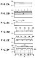
- Figures 2A - 2F are partially sectional views of a color liquid crystal display device according to a first embodiment of the present invention for sequentially illustrating production processes of the display device.
- Figures 3A - 3E are partially sectional views of a color liquid crystal display device according to a second embodiment of the present invention for sequentially illustrating production processes of the display device.
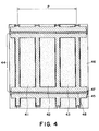
- Figure 4 is a plan view of a matrix electrode structure of a color liquid crystal display device according to a third embodiment and a fourth embodiment of the present invention.
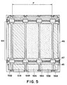
- Figures 5 and 6 are plan views each for illustrating arrangement of electrodes, a color filter and a light-interrupting layer used in color liquid crystal display devices according to a third embodiment and a fourth embodiment of the present invention, respectively.
- Figure 7 is a plan view for illustrating states of color displaying and light interruption in a third embodiment and a fourth embodiment of the present invention.
- Figure 8 is a plan view of a matrix electrode structure of a color liquid crystal display device according to a fifth embodiment and a sixth embodiment of the present invention.
- Figures 9 and 10 are plan views each for illustrating arrangement of electrodes, a color filter and a light-interrupting layer used in color liquid crystal display devices according to a fifth embodiment and a sixth embodiment of the present invention, respectively.
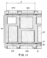
- Figure 11 is a plan view for illustrating states of color displaying and light interruption in a fifth embodiment and a sixth embodiment of the present invention.
- light interruption prevention of light passing or light leakage
- a first light-interrupting layer formed on a first substrate in combination with one or two second light-interrupting layers formed on the first substrate or/and a second substrate.
- the first light-interrupting layer comprises at least one layer comprising a material identical to that of at least one of plural color filter segments, whereby the first light-interrupting layer and the corresponding color filter segment(s) are formed at the same time, thus simplifying a device structure and a production process of the display device.
- the second light-interrupting layer comprises, e.g., a layer of auxiliary electrodes composed of a metallic material and disposed in contact with corresponding (first and/or second) transparent electrodes (as specifically described hereinafter).
- hue and reflection characteristics e.g., reflectivity
- the first light-interrupting layer exhibits a light-interrupting characteristic different from that of an ordinary black light-interrupting layer (black matrix) consisting of a metallic material generally used for light-interruption between color pixels. More specifically, as described above, the first light-interrupting layer functions so as to effectively suppress complete light transmission between adjacent color pixels in combination with the second light-interrupting layer by appropriately controlling a positional relationship therebetween and area ratios, thus substantially masking an entire spacing between color pixels as a whole.
- black matrix black matrix
- the first substrate provided with a color filter may preferably be disposed on the display face side (i.e., the observer (viewer) side).
- a substrate provided with a color filter (as the lower substrate 2 shown in Figure 1) is referred to as a "first substrate” and another substrate disposed opposite to (and spaced apart from) the substrate provided with the color filter (as the upper substrate 9 shown in Figure 1) is referred to as a "second substrate”.
- a second substrate has a structure similar to that of the upper substrate 9 shown in Figure 1 and explanation thereof is omitted.
- Figures 2A - 2F are sectional views of a first substrate 2 along a production process thereof specifically described hereinafter in this embodiment.
- a color liquid crystal display device 20 includes the first substrate 2 having a structure shown in Figure 2F.
- each of display pixels has a region P wherein a red color filter segment 3R (called “red filter”), a green color filter segment 3G (called “green filter”) and a blue color filter segment 3B (called “blue filter”) each constituting a color pixel and, e.g., comprising a colored resin are disposed.
- Adjacent (consecutive) display pixels are apart from each other with a prescribed spacing S.
- one of first light-interrupting layers 21R, 21G an 21B each comprising a material identical to that of each of color filter segments 3R, 3G and 3B, respectively, is arranged so that three species of the first light-interrupting layers (21R, 21G and 21B) are balanced with each other in dispersion density in a prescribed area and may preferably be disposed in the order of the layers 21R, 21G and 21B (not shown) as shown in Figure 2F. However, the arrangement of the layers 21R, 21G and 21B may be performed in different orders and manners, as desired.
- a passivation film (thin film) 5 is formed so as to cover (coat) the members 3R, 3G, 3B, 21R, 21G and 21B. Further, a group of transparent electrodes 6 are formed on the passivation film 5, and thereon, auxiliary electrodes 22 are disposed as shown in Figure 2F.
- Each of the auxiliary electrodes 22 comprises a material of a non-transparent metal and is disposed or arranged so that at least a portion of the auxiliary electrode 22 is located in a position corresponding to a spacing between the red filter 3R and the green filter 3G or between the green filter 3G and the blue filter 3B and so that the auxiliary electrodes 22 function as a second light-interrupting layer.
- the spacing S between the adjacent pixels and the spacing between the adjacent color filter segments (two color pixels) can be prevented from being subjected to light passage (light transmission) by the first light-interrupting layer (21R, 21B, 21G) and the second light-interrupting layer (auxiliary electrode 22) in combination, thus substantially allowing a necessary light interruption performance.
- additional auxiliary electrodes 22 may be disposed on the transparent substrate 6 (shown in Figure 2F) at both end portions thereof (masking spacings between 3R and 21R and between 3B and 21G) so as to perform complete light interruption at the spacings S between the pixels in combination with the first light-interrupting layers (21R, 21G and 21B) (not shown).
- a red pigment dispersion-type photosensitive resin as a color filter material 30 (polyamide-based resin, "PA-1013", available from Ube Kosan K.K.) is applied in a thickness of about 1.5 ⁇ m onto the surface of a first substrate 2 by a spinner (not shown) ( Figure 2A), followed by pre-baking of 10 minutes at 80 o C.
- the thus treated first substrate 2 is subjected to exposure to ultraviolet (UV) light at a light quantity of 300 - 600 mJ via a photomask 31 ( Figure 2B).
- UV ultraviolet
- the resultant first substrate 2 is subjected to development, rinse and post-baking of 10 minutes at 230 o C, thus forming a red filter (red color filter segment) 3R and a first light-interrupting layer 21R from an identical material at the same time ( Figure 2C).
- This step is repeatedly performed with respect to a green filter 3G and a first light-interrupting layer 21G for green (G) and a blue filter 3B and a first light-interrupting layer 21B for blue (B), respectively ( Figure 2D).
- a transparent resin 21 ("PA-1000C", available from Ube Kosan K.K.) is applied by a spinner (not shown) onto the above-treated first substrate 2 ( Figure 2E), followed by heating and curing the transparent resin 21 for 10 minutes at 230 o C to form an about 2 ⁇ m-thick passivation film 5.
- a group of transparent electrodes 6 are formed in a thickness of 1500 ⁇ by forming an ITO (indium tin oxide) film through sputtering and subjecting patterning through photolithographic steps ( Figure 2F).
- ITO indium tin oxide
- a 1500 ⁇ -thick molybdenum film is formed on the transparent electrode 6 by sputtering and subjected to patterning through photolithographic steps to provide auxiliary electrodes 22 (Figure 2F).
- a portion (central portion) of the auxiliary electrode 22 overlaps with a corresponding spacing between corresponding color filter segments (e.g., 3R and 3G) to suppress light leakage therebetween.
- an insulating layer and an alignment control layer may be formed as desired.
- a second substrate having thereon transparent electrodes and auxiliary electrodes (similar to the upper substrate 9 as shown in Figure 1) optionally provided with an insulating layer and an alignment control layer, as desired, is prepared in a similar manner as in the first substrate 2.
- the first and second substrates are disposed opposite to and spaced apart from each other with a prescribed gap (cell gap) while causing the groups of transparent electrodes on the first and second substrates to intersect with each other at right angles to provide a matrix electrode structure so as to form plural color pixels each at a region of an intersection of the groups of the transparent electrodes superposed with the plural color filters (color filter segments) while leaving a pixel spacing (e.g., the spacing S or the spacing between 3R and 3G) between the plural color pixels.
- the gap is filled with a liquid crystal to provide a color liquid crystal display device.
- a light (backlight) issued from the backlight apparatus passes through (transmits) the color filter (color filter segments 3R, 3G and 3B) to allow various color display states by various transmitted light components in combination.
- the first light-interrupting layer (21R, 21G, 21B) is disposed at a portion of the pixel spacing (the spacing S) between adjacent display pixels and the auxiliary electrodes 22 a the second light-interrupting layer are disposed so as to mask a remaining portion of the pixel spacing (e.g., a spacing between adjacent color filter segments 3R and 3G), thus substantially masking the entire pixel spacing (i.e., substantially preventing leakage of incident light (from the backlight apparatus) at the entire pixel spacings between the color pixels including those between the display pixels) at a practically acceptable level although the first light-interrupting layer partially transmits the incident light.
- resultant display images are excellent in contrast and display quality.
- a light-interrupting member exclusively used for light interruption (e.g., a metal layer of, e.g., chromium (Cr), particularly disposed between color filter segments, such as the layer 12 as shown in Figure 1) since the fist and second light-interrupting layers used in the present invention are composed of a material identical to the color filter segment material and the auxiliary electrode, respectively, so that a structure and production process of the resultant color liquid crystal display device are simplified to lower production costs. It is also possible to improve a product yield.
- a light-interrupting member exclusively used for light interruption (e.g., a metal layer of, e.g., chromium (Cr), particularly disposed between color filter segments, such as the layer 12 as shown in Figure 1) since the fist and second light-interrupting layers used in the present invention are composed of a material identical to the color filter segment material and the auxiliary electrode, respectively, so that a structure and production process of the resultant color liquid crystal display device are simplified to lower production costs. It
- the first light-interrupting layer (21R, 21G, 21B) may preferably be arranged suitably in view of a color balance with respect to a prescribed area, whereby no image display region locally takes on a certain color.
- the first substrate (provided with the color filter segments) is disposed on the viewer side
- external light reflection can effectively be prevented since the first light-interrupting layer employs a non-metallic material and the second light-interrupting layer comprising the molybdenum film is located behind the color filter segments via the passivation film and the transparent electrodes when viewed from the viewer side. Consequently, on the display face, good display characteristics can be attained based on a uniform reflection state.
- Figures 3A - 3E are sectional views of a first substrate 2 along a production process thereof.
- a color liquid crystal display device is formed in the similar manner as in the first embodiment described above except that a first light-interrupting layer is consisting of three layers 21R, 21G and 21B each provided with a width of 3 ⁇ m together disposed at a prescribed spacing (a portion of a pixel spacing) corresponding to the spacing S in Figure 2F. More specifically, a color filter segment and a layer having a color identical to the color filter segment (3R and 21R; 3G and 21G; or 3B and 21B) are formed at the same time through the photolithographic steps. Further, other members, such as transparent electrodes 6 and auxiliary electrodes 22 as a second light-interrupting layer are formed similarly as in the first embodiment.
- the first light-interrupting layer composed of a set of three layers 21R, 21G and 21B (for red, green and blue, respectively) is disposed at the prescribed spacing between adjacent two display pixels so as to display white as a whole when incident light from a backlight apparatus (not shown) passes through the prescribed portion.
- additional auxiliary electrodes 22 may be disposed on the transparent substrate 6 (shown in Figure 3E) at both end portions thereof (masking spacings between 3R and 21B and between 3B and 21R) so as to perform substantially complete light interruption at the spacings (corresponding to the spacings S as in Figure 2F) between the pixels in combination with the first light-interrupting layers (21R, 21G and 21B).
- the first light-interrupting layer is arranged so as to provide a set of three colored layers (21R for red, 21G for green and 21B for blue) per each spacing S, so that an image display region is not locally changed to have a particular color.
- the first light-interrupting layer (21R, 21G and 21B) masks a portion of the pixel spacing between adjacent two display pixels (each having a region P) and the second light-interrupting layer (auxiliary electrodes 22) masks a remaining portion of the pixel spacing between color pixels.
- the second light-interrupting layer masks the above portion of the pixel spacing (between adjacent two display pixels) and the first light-interrupting layer masks the remaining portion of the pixel spacing.
- the pixel spacing between the color pixels is masked with the (first and second) light-interrupting layers formed on an identical (first) substrate having the color filter segments.
- the second substrate it is possible to provide the second substrate with a (second) light-interrupting layer in the first and second embodiments.
- a light-interrupting member (first and second light-interrupting layers) provided to a first substrate and a light-interrupting member (second light-interrupting layer) provided to a second (opposite) substrate as a whole mask an entire pixel spacing between color pixels.
- Figure 4 is a plan view showing a matrix electrode structure formed by (first and second) transparent electrodes provided to a pair of (first and second) substrates adopted in color liquid crystal display devices according to third and fourth embodiments of the present invention. Specifically, Figure 4 shows a state of arrangement of respective transparent and auxiliary electrodes viewed from the first substrate (to be provided with color filter segments) side.
- a group of (first) transparent electrodes (not shown) in the form of stripes (transparent electrode pattern) each having a width 44 are formed and thereon a group of auxiliary electrodes (auxiliary electrode pattern) 45 comprising a non-(light) transmissive material, such as metal are formed so as to contact or cover (coat) the transparent electrodes.
- plural color filter segments are disposed in superposition with (preferably below or under) the (first) transparent electrodes so as to overlap regions 41, 42 and 43 defined by the transparent electrode pattern (not shown) having the width 44 and the auxiliary electrode pattern 45.
- a group of (second) transparent electrodes (transparent electrode pattern) 46 are formed so as to intersect with the (first) transparent electrodes to constitute a matrix electrode structure.
- a group of auxiliary electrodes (auxiliary electrode pattern) 47 comprising a non-transmissive material (e.g., metal) are formed so s to contact or cover the transparent electrodes 46.
- first and second substrates On each of the first and second substrates, several layers (not shown) including an insulating layer and an alignment control layer (for controlling alignment of liquid crystal molecules) are formed so as to cover the respective transparent and auxiliary electrodes.
- the first and second substrates treated as described above are caused to be opposite to and spaced apart from each other to provide a prescribed gap (cell gap), which is then filled with a liquid crystal to prepare a color liquid crystal display device (not shown).
- the color liquid crystal display device having the matrix electrode structure contain display pixels each having a length (width) P and a width (length) 44 and including three color pixels 41, 42 and 43 and a pixel spacing between the color pixels.
- the entire pixel spacing (between the color pixels including between the adjacent display pixels) except for regions 48 in Figure 4 is masked with the auxiliary electrode patterns 45 and 47 (functioning as the second light-interrupting layer).
- the regions 48 (a remaining portion of the pixel spacing) are masked with a first light-interrupting layer comprising a material identical to that of at least one of the plural color filter segments as described hereinbelow (third and fourth embodiments).
- Figure 5 is a plan view of a color liquid crystal display device according to a third embodiment of the present invention wherein an arrangement of transparent and auxiliary electrodes, color filter segments, and a light-interrupting member viewed from the first substrate side is specifically shown.
- three color filter segments including a red filter 51R, a green filter 52G and a blue filter 53B per one display pixel are formed and disposed in a position closer to the first substrate than the first transparent electrodes.
- the three color filter segments 51R, 52G and 53B are arranged so as to correspond to the regions (color pixels) 41, 42 and 43 (shown in Figure 4), respectively.
- a (first) light-interrupting member (layer) including a layer 54R comprising a material identical to that of the red filter 51R, a layer 55G comprising a material identical to that of the green filter 52G, and a layer 56B comprising a material identical to that of the blue filter 53B are formed so as to mask the regions 48 (shown in Figure 4) simultaneously with and preferably on an identical level with the color filter segments 51R, 52G and 53B in an identical step.
- the entire pixel spacing defined by the color pixels 41, 42 and 43 ( Figure 4) and not contributing to (color) display is substantially masked (covered) with the light-interrupting member (the layers 54R, 55G and 56B) and auxiliary electrode pattern 45 provided to the first substrate and the auxiliary electrode pattern 47 provided to the second substrate in combination by preventing leakage (escape) of light from the pixel spacing.
- the light-interrupting layers 54R, 55G and 56B and the color filter segments 51R, 52G and 53B are formed at the same time by using the identical materials (e.g., non-metallic colored resins) respectively, whereby a production process and a device structure are simplified.
- the auxiliary electrode patterns 45 and 47 are disposed sufficiently behind the display face when the device is viewed from the first substrate side, an excessive external light reflection (due to external light from the viewer side in a light (sunny) place) can effectively be suppressed.
- Figure 6 is a plan view of a fourth embodiment of the color liquid crystal display device according to the present invention similar to Figure 5 except for employing ia different first light-interrupting member (layer), wherein identical structural members used in the third and fourth embodiments are indicated by identical reference numerals.
- a blue color filter segment (blue filter) 53B formed on the first substrate extends to a region 60 between first transparent electrodes (formed on the first substrate) each having a width 44 and functions as a (first) light-interrupting layer masking a peripheral portion (including the regions 48 shown in Figure 4) of each display pixel, thus masking the entire pixel spacing as a whole together with an auxiliary electrode pattern 45 formed on the first substrate and an auxiliary electrode pattern 47 formed on the second substrate.
- the first light-interrupting layer masking the regions 48 is only consisting of the blue filter 53B providing the lowest (light) transmittance with respect to an identical filter thickness (herein, "transmittance” refers to one given under thus condition) among the color filters 51R, 52G and 53B, thus further effectively suppressing light leakage.
- Figure 7 is a plan view for illustrating how to effect color display and light-interruption (masking) in the above-described third and fourth embodiments.
- color display is performed by using three color filter segments (red filter 51R, green filter 52G, and blue filter 53B) singly or in combination of two or three filters.
- a pixel spacing between color pixels (41 to 43 shown in Figure 4) is principally masked with auxiliary electrode patterns 45 and 47 formed on first and second substrates, respectively. Further, small regions 61 remaining as a portion of the pixel spacing are masked with the light-interrupting layers 54R, 55G and 56B shown in Figure 5 (Third Embodiment) or with the blue filter 53B shown in Figure 6 (Fourth Embodiment).
- the entire pixel spacing is substantially light-interrupted by preventing leakage of incident light from the backlight apparatus.
- Figure 8 is a plan view showing a matrix electrode structure formed by (first and second) transparent electrodes provided to a pair of (first and second) substrates adopted in color liquid crystal display devices according to fifth and sixth embodiments of the present invention. Specifically, Figure 8 shows a state of arrangement of respective transparent and auxiliary electrodes viewed from the first substrate (to be provided with color filter segments) side.
- the device structure is principally similar to that shown in Figure 4 except that four regions 41, 42, 43 and 49 are provided per one display pixel (having widths P and 44), wherein structural members identical to those shown in Figure 4 are indicated by identical reference numerals.
- the four regions 41, 42, 43 and 49 are defined by the (first) transparent electrode pattern (having the width 44) and the auxiliary electrode patterns 45 and 47.
- Four color filter segments (not shown) of red, green, blue and white are disposed so as to overlap the four regions 41, 42, 43 and 49, respectively, as shown in Figures 9 - 11.
- Figure 9 is a plan view of a color liquid crystal display device according to a fifth embodiment of the present invention wherein an arrangement of transparent and auxiliary electrodes, color filter segments, and a light-interrupting member is specifically shown similarly as in Figure 8.
- each color filter segment including a red filter 51R, a green filter 52G, a blue filter 53B and a white (clear) filter 57W per one display pixel are formed and disposed in a position closer to the first substrate than the first transparent electrodes.
- the four color filter segments 51R, 52G, 53B and 57W are arranged so as to correspond to the regions (color pixels) 41, 42, 43 and 49 (shown in Figure 8), respectively.
- a (first) light-interrupting member (layer) including a layer 54R comprising a material identical to that of the red filter 51R and a layer 56B comprising a material identical to that of the blue filter 53B are formed so as to mask regions 48 (shown in Figure 8) simultaneously with and preferably on an identical level with the color filter segments 51R and 53B in an identical step.
- the entire pixel spacing defined by the color pixels 41, 42, 43 and 49 ( Figure 8) and not contributing to (color) display is substantially masked (covered) with the light-interrupting member (the layers 54R and 56B) and auxiliary electrode pattern 45 provided to the first substrate and the auxiliary electrode pattern 47 provided to the second substrate in combination by preventing leakage (escape) of light from the pixel spacing.
- Figure 10 is a plan view of a sixth embodiment of the color liquid crystal display device according to the present invention similar to Figure 9 except for employing ia different first light-interrupting member (layer).
- a blue color filter segment (blue filter) 53B formed on the first substrate extends to a region between first transparent electrodes (formed on the first substrate) each having a width 44 and functions as a (first) light-interrupting layer masking a peripheral portion (including the regions 48 shown in Figure 8) of each display pixel, thus masking the entire pixel spacing as a whole together with an auxiliary electrode pattern 45 formed on the first substrate and an auxiliary electrode pattern 47 formed on the second substrate.
- the first light-interrupting layer masking the regions 48 is only consisting of the blue filter 53B providing the lowest (light) transmittance among the color filters 51R, 52G, 53B and 57W, thus effectively suppressing light leakage.
- Figure 11 is a plan view for illustrating how to effect color display and light-interruption (masking) in the above-described fifth and sixth embodiments.
- color display is performed by using three color filter segments (red filter 51R, green filter 52G, blue filter 53B and white filter 57W) singly or in combination of two to four filters.
- a pixel spacing between color pixels (41, 42, 43 and 49 shown in Figure 8) is principally masked with auxiliary electrode patterns 45 and 47 formed on first and second substrates, respectively. Further, small regions 61 (regions 48 in Figure 8) remaining as a portion of the pixel spacing are masked with the light-interrupting layers 54R and 56B shown in Figure 9 (Fifth Embodiment) or with the extended blue filter 53B shown in Figure 10 (Sixth Embodiment). As a result, the entire pixel spacing is substantially light-interrupted by preventing leakage of incident light from the backlight apparatus.
- the fifth and sixth embodiments of the color liquid crystal display devices of the present invention it is possible to attain effects similar to those in the third and fourth embodiments described above, respectively.
- the light-interrupting layer (54R and 56B in the fifth embodiment or 53B in the sixth embodiment) and the color filter segments 51R, 52G, 53B and 57W are formed at the same time with respect to identical colors by using the identical materials (e.g., non-metallic colored resins) respectively, whereby a production process and a device structure are simplified.
- auxiliary electrode patterns 45 and 47 are disposed sufficiently behind the display face when the device is viewed from the first substrate side, an excessive external light reflection (due to external light from the viewer side in a light (sunny) place) can effectively be suppressed.
- the regions (48 in Figure 8 or 61 in Figure 11) which cannot be masked with the auxiliary electrode patterns 45 and 47 are masked with the light-interrupting layer comprising the layer 56B assuming blue (providing the lowest transmittance among the four colors) and the layer 54R assuming red (providing the second lowest transmittance) in the fifth embodiment or masked with the light-interrupting layer (the blue color filter segment 53B) providing the lowest transmittance, thus further effectively preventing light leakage at the pixel spacing compared with the case of using a light-interrupting member including layers assuming other colors.
- the color liquid crystal display device it is possible to use various liquid crystal materials including those of a twisted nematic (TN) type, those of a super-twisted nematic (STN) type, and those assuming chiral smectic phase. Further, in the above-described first to sixth embodiments, a simple matrix-type liquid crystal display device is employed but an active matrix-type liquid crystal display device using, e.g., a thin film transistor (TFT) may be adopted.
- TFT thin film transistor
- the color liquid crystal display device and the process for producing the device according to the present invention provide the following advantages (i) to (iv).
- the first substrate is provided with a first light-interrupting layer comprising a material identical to that of at least one of the plural color filter segments and disposed at a portion of the pixel spacing so as to mask the portion, and at least one of the first and second substrates is provided with a second light-interrupting layer masking a remaining portion of the pixel spacing.
- the first and second light-interrupting layers as a whole are effective in preventing leakage of light between color pixels, thus providing images with a high contrast and an excellent display quality.
Landscapes
- Physics & Mathematics (AREA)
- Nonlinear Science (AREA)
- Mathematical Physics (AREA)
- Chemical & Material Sciences (AREA)
- Crystallography & Structural Chemistry (AREA)
- General Physics & Mathematics (AREA)
- Optics & Photonics (AREA)
- Liquid Crystal (AREA)
- Optical Filters (AREA)
- Optical Elements Other Than Lenses (AREA)
Applications Claiming Priority (4)
| Application Number | Priority Date | Filing Date | Title |
|---|---|---|---|
| JP179165/95 | 1995-07-14 | ||
| JP17916595 | 1995-07-14 | ||
| JP181033/96 | 1996-07-10 | ||
| JP18103396A JP3296719B2 (ja) | 1995-07-14 | 1996-07-10 | カラー液晶表示素子及び該カラー液晶表示素子の製造方法 |
Publications (1)
| Publication Number | Publication Date |
|---|---|
| EP0753783A1 true EP0753783A1 (de) | 1997-01-15 |
Family
ID=26499101
Family Applications (1)
| Application Number | Title | Priority Date | Filing Date |
|---|---|---|---|
| EP96111401A Withdrawn EP0753783A1 (de) | 1995-07-14 | 1996-07-15 | Farbige Flüssigkristallanzeige und deren Herstellungsverfahren |
Country Status (3)
| Country | Link |
|---|---|
| US (1) | US5777707A (de) |
| EP (1) | EP0753783A1 (de) |
| JP (1) | JP3296719B2 (de) |
Cited By (2)
| Publication number | Priority date | Publication date | Assignee | Title |
|---|---|---|---|---|
| WO1999018475A1 (de) * | 1997-10-07 | 1999-04-15 | Robert Bosch Gmbh | Flüssigkristallzelle |
| CN102369788A (zh) * | 2009-04-09 | 2012-03-07 | 松下电器产业株式会社 | 有机电致发光显示装置 |
Families Citing this family (21)
| Publication number | Priority date | Publication date | Assignee | Title |
|---|---|---|---|---|
| US6320639B1 (en) * | 1996-03-11 | 2001-11-20 | Canon Kabushiki Kaisha | Liquid crystal device and process for production thereof |
| US5943108A (en) * | 1996-07-12 | 1999-08-24 | Canon Kabushiki Kaisha | Matrix type liquid crystal display with substrate having blue filter for masking at least 75% of total planar area of auxiliary electrodes |
| US5899550A (en) * | 1996-08-26 | 1999-05-04 | Canon Kabushiki Kaisha | Display device having different arrangements of larger and smaller sub-color pixels |
| JP3392672B2 (ja) * | 1996-11-29 | 2003-03-31 | 三洋電機株式会社 | 表示装置 |
| US6184962B1 (en) | 1997-03-05 | 2001-02-06 | Canon Kabushiki Kaisha | Liquid crystal display device with visible peripheral non-display region having masking sub-electrodes |
| JPH10268300A (ja) * | 1997-03-21 | 1998-10-09 | Sony Corp | 反射型ゲストホスト液晶表示装置 |
| US6081309A (en) * | 1997-08-28 | 2000-06-27 | Canon Kabushiki Kaisha | Liquid crystal device |
| US6271907B1 (en) | 1997-09-14 | 2001-08-07 | Canon Kabushiki Kaisha | Color liquid crystal device having injection port parallel to the stripe electrodes on the substrate with color filter and flattening film and the other substrate free from color filter and flattening film protruded |
| US7090890B1 (en) | 1998-04-13 | 2006-08-15 | The Trustees Of Princeton University | Modification of polymer optoelectronic properties after film formation by impurity addition or removal |
| KR100604717B1 (ko) * | 1999-07-08 | 2006-07-28 | 엘지.필립스 엘시디 주식회사 | 액정 표시장치 제조방법 및 그 제조방법에 따른 액정표시장치 |
| US7116378B1 (en) * | 2000-08-15 | 2006-10-03 | Displaytech, Inc. | Color-balanced brightness enhancement for display systems |
| US7046221B1 (en) * | 2001-10-09 | 2006-05-16 | Displaytech, Inc. | Increasing brightness in field-sequential color displays |
| KR100978254B1 (ko) * | 2003-06-30 | 2010-08-26 | 엘지디스플레이 주식회사 | 4화소구조 횡전계모드 액정표시소자 |
| KR101157223B1 (ko) * | 2003-10-29 | 2012-06-15 | 엘지디스플레이 주식회사 | 횡전계방식 액정표시소자 및 그 제조방법 |
| KR101068019B1 (ko) * | 2003-10-29 | 2011-09-26 | 엘지디스플레이 주식회사 | 횡전계방식 액정표시소자 및 그 제조방법 |
| KR100554911B1 (ko) * | 2003-12-26 | 2006-02-24 | 엘지.필립스 엘시디 주식회사 | 액정표시장치 |
| JP4548475B2 (ja) | 2007-11-20 | 2010-09-22 | ソニー株式会社 | 液晶表示素子および投射型液晶表示装置 |
| KR101579487B1 (ko) * | 2008-10-28 | 2015-12-23 | 삼성디스플레이 주식회사 | 표시 장치 |
| KR101269006B1 (ko) * | 2008-12-02 | 2013-05-29 | 엘지디스플레이 주식회사 | 액정표시장치 |
| TW201200948A (en) | 2010-06-22 | 2012-01-01 | Au Optronics Corp | Pixel structure and method for manufacturing the same |
| US10690970B2 (en) | 2016-04-08 | 2020-06-23 | Apple Inc. | Display with hybrid column spacer structures |
Citations (4)
| Publication number | Priority date | Publication date | Assignee | Title |
|---|---|---|---|---|
| JPS62250416A (ja) * | 1986-04-23 | 1987-10-31 | Stanley Electric Co Ltd | Tft組込型カラ−液晶表示素子 |
| JPS62294222A (ja) * | 1986-06-13 | 1987-12-21 | Seiko Epson Corp | 液晶表示体の遮光部の製造方法 |
| US4853296A (en) * | 1986-10-22 | 1989-08-01 | Toppan Printing Co., Ltd. | Electrode plate for color display device |
| EP0473168A2 (de) * | 1990-08-30 | 1992-03-04 | Canon Kabushiki Kaisha | Flüssigkristallvorrichtung |
Family Cites Families (15)
| Publication number | Priority date | Publication date | Assignee | Title |
|---|---|---|---|---|
| DE3113041A1 (de) * | 1980-04-01 | 1982-01-28 | Canon K.K., Tokyo | Verfahren und vorrichtung zur anzeige von informationen |
| JPS59129832A (ja) * | 1983-01-18 | 1984-07-26 | Canon Inc | 光学変調装置 |
| JP2576483B2 (ja) * | 1987-01-26 | 1997-01-29 | セイコーエプソン株式会社 | カラーフィルター |
| EP0326112B1 (de) * | 1988-01-29 | 1994-09-14 | Toppan Printing Co., Ltd. | Elektrodenstruktur für Anzeigevorrichtungen und ihr Herstellungsverfahren |
| JP2673739B2 (ja) * | 1990-07-31 | 1997-11-05 | キヤノン株式会社 | 液晶素子 |
| JP2700945B2 (ja) * | 1990-08-30 | 1998-01-21 | キヤノン株式会社 | カラーフィルター付き基板 |
| US5282068A (en) * | 1990-11-08 | 1994-01-25 | Canon Kabushiki Kaisha | Liquid crystal display with opaque insulating layer and metal layer at and wider than inter-electrode gap and method of manufacturing |
| JPH04317027A (ja) * | 1991-04-16 | 1992-11-09 | Seiko Instr Inc | 多色表示装置 |
| US5285300A (en) * | 1991-10-07 | 1994-02-08 | Canon Kabushiki Kaisha | Liquid crystal device |
| JP2974520B2 (ja) * | 1991-10-25 | 1999-11-10 | キヤノン株式会社 | 電極基板及び液晶素子 |
| JP3350991B2 (ja) * | 1992-03-06 | 2002-11-25 | セイコーエプソン株式会社 | 電気光学装置用基板、及び電気光学装置 |
| JP2543286B2 (ja) * | 1992-04-22 | 1996-10-16 | インターナショナル・ビジネス・マシーンズ・コーポレイション | 液晶表示装置 |
| US5461501A (en) * | 1992-10-08 | 1995-10-24 | Hitachi, Ltd. | Liquid crystal substrate having 3 metal layers with slits offset to block light from reaching the substrate |
| JP2596692B2 (ja) * | 1993-03-02 | 1997-04-02 | インターナショナル・ビジネス・マシーンズ・コーポレイション | 散乱型液晶表示装置 |
| JPH06331974A (ja) * | 1993-05-26 | 1994-12-02 | Canon Inc | カラー液晶表示装置 |
-
1996
- 1996-07-10 JP JP18103396A patent/JP3296719B2/ja not_active Expired - Fee Related
- 1996-07-15 US US08/679,988 patent/US5777707A/en not_active Expired - Lifetime
- 1996-07-15 EP EP96111401A patent/EP0753783A1/de not_active Withdrawn
Patent Citations (4)
| Publication number | Priority date | Publication date | Assignee | Title |
|---|---|---|---|---|
| JPS62250416A (ja) * | 1986-04-23 | 1987-10-31 | Stanley Electric Co Ltd | Tft組込型カラ−液晶表示素子 |
| JPS62294222A (ja) * | 1986-06-13 | 1987-12-21 | Seiko Epson Corp | 液晶表示体の遮光部の製造方法 |
| US4853296A (en) * | 1986-10-22 | 1989-08-01 | Toppan Printing Co., Ltd. | Electrode plate for color display device |
| EP0473168A2 (de) * | 1990-08-30 | 1992-03-04 | Canon Kabushiki Kaisha | Flüssigkristallvorrichtung |
Non-Patent Citations (2)
| Title |
|---|
| PATENT ABSTRACTS OF JAPAN vol. 012, no. 125 (P - 691) 19 April 1988 (1988-04-19) * |
| PATENT ABSTRACTS OF JAPAN vol. 012, no. 185 (P - 710) 31 May 1988 (1988-05-31) * |
Cited By (5)
| Publication number | Priority date | Publication date | Assignee | Title |
|---|---|---|---|---|
| WO1999018475A1 (de) * | 1997-10-07 | 1999-04-15 | Robert Bosch Gmbh | Flüssigkristallzelle |
| CN102369788A (zh) * | 2009-04-09 | 2012-03-07 | 松下电器产业株式会社 | 有机电致发光显示装置 |
| EP2429263A4 (de) * | 2009-04-09 | 2013-09-04 | Panasonic Corp | Organische elektrolumineszenzanzeigevorrichtung |
| US8564196B2 (en) | 2009-04-09 | 2013-10-22 | Panasonic Corporation | Organic electroluminescent display device containing filter to provide high contrast |
| CN102369788B (zh) * | 2009-04-09 | 2014-06-11 | 松下电器产业株式会社 | 有机电致发光显示装置 |
Also Published As
| Publication number | Publication date |
|---|---|
| JPH0990343A (ja) | 1997-04-04 |
| US5777707A (en) | 1998-07-07 |
| JP3296719B2 (ja) | 2002-07-02 |
Similar Documents
| Publication | Publication Date | Title |
|---|---|---|
| US5777707A (en) | Color liquid crystal display device and process for producing same | |
| EP0715202B1 (de) | Anzeigevorrichtung | |
| US5757452A (en) | Color liquid crystal panel with light shielding layer sections formed between color filter films without contacting said color filter films | |
| US6147728A (en) | Reflective color LCD with color filters having particular transmissivity | |
| EP0303852B1 (de) | Farbige Flüssigkristallanzeige und Verfahren zu deren Herstellung | |
| KR100907479B1 (ko) | 컬러 필터 기판과 이를 갖는 액정 표시 장치 | |
| US6704075B2 (en) | Color filter substrate, method of fabricating color filter substrate, liquid crystal device, method of fabricating liquid crystal device, and electronic apparatus | |
| KR100989339B1 (ko) | 액정표시장치 및 이의 제조 방법 | |
| US7545466B2 (en) | Liquid crystal display device and substrate therefor | |
| KR20000057974A (ko) | 컬러 필터 및 광학적 표시 장치 | |
| JP3625396B2 (ja) | 表示装置 | |
| JP2806741B2 (ja) | カラー液晶ディスプレイ | |
| KR100965193B1 (ko) | 액정표시장치 | |
| US5943109A (en) | Liquid crystal display device formed with a hologram layer having a plurality of patterns | |
| US8120732B2 (en) | Liquid crystal display device with different liquid crystal layer thicknesses corresponding to different color regions | |
| US11281043B2 (en) | Display panel and display apparatus | |
| JP3040943B2 (ja) | カラーフィルター基板及びそれを用いた液晶素子 | |
| JP3776022B2 (ja) | カラー液晶表示装置 | |
| US5943108A (en) | Matrix type liquid crystal display with substrate having blue filter for masking at least 75% of total planar area of auxiliary electrodes | |
| JPH08220527A (ja) | カラーフィルタ基板とその製造方法および液晶表示装置 | |
| JP3245008B2 (ja) | カラー液晶表示装置およびその製造方法 | |
| KR101068354B1 (ko) | 액정표시장치 및 그 제조방법 | |
| JP3981321B2 (ja) | 液晶パネルおよび該液晶パネルを備える液晶表示装置 | |
| JPH0990339A (ja) | 液晶表示装置 | |
| JP2004151309A (ja) | 半透過型カラー液晶表示装置 |
Legal Events
| Date | Code | Title | Description |
|---|---|---|---|
| PUAI | Public reference made under article 153(3) epc to a published international application that has entered the european phase |
Free format text: ORIGINAL CODE: 0009012 |
|
| 17P | Request for examination filed |
Effective date: 19960715 |
|
| AK | Designated contracting states |
Kind code of ref document: A1 Designated state(s): DE FR GB IT NL |
|
| GRAH | Despatch of communication of intention to grant a patent |
Free format text: ORIGINAL CODE: EPIDOS IGRA |
|
| STAA | Information on the status of an ep patent application or granted ep patent |
Free format text: STATUS: THE APPLICATION IS DEEMED TO BE WITHDRAWN |
|
| 18D | Application deemed to be withdrawn |
Effective date: 20030816 |