EP0756932A2 - Verfahren zum Herstellen eines Farbfilters, Farbfilter, Anzeigevorrichtung und Apparat mit dieser Anzeigevorrichtung - Google Patents
Verfahren zum Herstellen eines Farbfilters, Farbfilter, Anzeigevorrichtung und Apparat mit dieser Anzeigevorrichtung Download PDFInfo
- Publication number
- EP0756932A2 EP0756932A2 EP96112360A EP96112360A EP0756932A2 EP 0756932 A2 EP0756932 A2 EP 0756932A2 EP 96112360 A EP96112360 A EP 96112360A EP 96112360 A EP96112360 A EP 96112360A EP 0756932 A2 EP0756932 A2 EP 0756932A2
- Authority
- EP
- European Patent Office
- Prior art keywords
- ink
- color
- jet head
- substrate
- discharge
- Prior art date
- Legal status (The legal status is an assumption and is not a legal conclusion. Google has not performed a legal analysis and makes no representation as to the accuracy of the status listed.)
- Granted
Links
Images











Classifications
-
- G—PHYSICS
- G02—OPTICS
- G02F—OPTICAL DEVICES OR ARRANGEMENTS FOR THE CONTROL OF LIGHT BY MODIFICATION OF THE OPTICAL PROPERTIES OF THE MEDIA OF THE ELEMENTS INVOLVED THEREIN; NON-LINEAR OPTICS; FREQUENCY-CHANGING OF LIGHT; OPTICAL LOGIC ELEMENTS; OPTICAL ANALOGUE/DIGITAL CONVERTERS
- G02F1/00—Devices or arrangements for the control of the intensity, colour, phase, polarisation or direction of light arriving from an independent light source, e.g. switching, gating or modulating; Non-linear optics
- G02F1/01—Devices or arrangements for the control of the intensity, colour, phase, polarisation or direction of light arriving from an independent light source, e.g. switching, gating or modulating; Non-linear optics for the control of the intensity, phase, polarisation or colour
- G02F1/13—Devices or arrangements for the control of the intensity, colour, phase, polarisation or direction of light arriving from an independent light source, e.g. switching, gating or modulating; Non-linear optics for the control of the intensity, phase, polarisation or colour based on liquid crystals, e.g. single liquid crystal display cells
- G02F1/133—Constructional arrangements; Operation of liquid crystal cells; Circuit arrangements
- G02F1/1333—Constructional arrangements; Manufacturing methods
- G02F1/1335—Structural association of cells with optical devices, e.g. polarisers or reflectors
- G02F1/133509—Filters, e.g. light shielding masks
- G02F1/133514—Colour filters
- G02F1/133516—Methods for their manufacture, e.g. printing, electro-deposition or photolithography
-
- B—PERFORMING OPERATIONS; TRANSPORTING
- B41—PRINTING; LINING MACHINES; TYPEWRITERS; STAMPS
- B41J—TYPEWRITERS; SELECTIVE PRINTING MECHANISMS, i.e. MECHANISMS PRINTING OTHERWISE THAN FROM A FORME; CORRECTION OF TYPOGRAPHICAL ERRORS
- B41J2/00—Typewriters or selective printing mechanisms characterised by the printing or marking process for which they are designed
- B41J2/005—Typewriters or selective printing mechanisms characterised by the printing or marking process for which they are designed characterised by bringing liquid or particles selectively into contact with a printing material
- B41J2/01—Ink jet
-
- B—PERFORMING OPERATIONS; TRANSPORTING
- B41—PRINTING; LINING MACHINES; TYPEWRITERS; STAMPS
- B41J—TYPEWRITERS; SELECTIVE PRINTING MECHANISMS, i.e. MECHANISMS PRINTING OTHERWISE THAN FROM A FORME; CORRECTION OF TYPOGRAPHICAL ERRORS
- B41J2202/00—Embodiments of or processes related to ink-jet or thermal heads
- B41J2202/01—Embodiments of or processes related to ink-jet heads
- B41J2202/09—Ink jet technology used for manufacturing optical filters
Definitions
- This invention relates to a color-filter manufacturing method and apparatus for manufacturing a color filter by discharging ink from an ink-jet head on a substrate, thus coloring respective pixels with a plurality of discharge ink, a color filter, a display device, and an apparatus having the display device.
- LCDs liquid-crystal displays
- color LCDs color LCDs
- the most popular first method is a coloring method.
- This method forms an RGB color filter layer by: (1) applying water-soluble polymer material as coloring material onto a glass substrate; (2) patterning a desired shape by a photolithography process; (3) dipping the obtained pattern into a coloring bath; and (4) repeating the process through steps (1) to (3) thrice.
- the second method is a pigment-dispersion method which is replacing the coloring method.
- This method forms an RGB color filter layer by: (1) forming a photosensitive resin layer where pigment is dispersed on a substrate; (2) patterning a pattern for single color; and (3) repeating the process through steps (1) and (2) thrice.
- the fourth method is a printing method.
- This method forms an RGB color filter by: (1) dispersing, as printing, pigment on thermosetting resin; (2) repeating printing thrice to apply three R, G and B colors; and (3) heat-setting the resin to form colored layer.
- any of these methods usually forms a protective layer on the colored layer.
- a common problem to these methods is to repeat the same process with respect to three R, G and B colors, which increases costs.
- the yield decreases.
- the electrodeposition method as the formable pattern shapes are limited, the technique cannot be applied to manufacture of TFTs.
- the printing method as resolution and smoothness in printing are poor, fine-pitch patterns cannot be formed.
- the ink is discharged from an ink-jet head in the form of droplets. Accordingly, ink droplets are separated from discharge nozzles at irregular timings, which causes variation in ink-discharge speeds at the respective discharge nozzles. While scanning the ink-jet head, otherwise scanning a stage under a fixed ink-jet head for coloring a color-filter substrate, this variation in ink-discharge speeds might shift ink-arrival positions on the color-filter substrate, thus might cause mixture of colors due to ink-arrival at a neighboring position to a target position, or cause uncolored portion(s) due to omission of coloring a desired pixel.
- Japanese Patent Application Laid-Open No. 61-274949 or Japanese Patent Application Laid-Open No. 4-129746 discloses, not discharging ink in the form of ink droplets, but applying ink in the form of pillars before the ink separate from the nozzles of the ink-jet head.
- ink in the form of pillars are applied to a coloring object, ink portion unnecessary for actual coloring is drawn back into the nozzles when the ink is separated from the nozzles.
- this method does not discharge ink droplets in the air, it is advantageous in the point that only low drive energy is required.
- the ink is not separated from the discharge nozzles in the form of droplets, the aforementioned variation in ink-discharge speeds due to shifting of ink-separation timings does not occur.
- Japanese Patent Application Laid-Open No. 61-274949 and Japanese Patent Application Laid-Open No. 4-129746 are directed to printing on recording media such as print sheets, but none of them discloses application to manufacture of color-filters.
- the present invention has been made in consideration of the above situation, and has its object to provide a color-filter manufacturing method and apparatus which manufactures a color filter while preventing mixture of colors or omission of coloring, with improvement in ink-arrival precision on a color-filter substrate.
- Another object of the present invention is to provide a color filter without color mixture or uncolored pixel(s), a display device using the color filter, and an apparatus having the display device.
- a color-filter manufacturing method for manufacturing a color filter by discharging ink from an ink-jet head on a substrate so as to color respective pixels with a plurality of discharge ink comprising the step of: discharging ink, not in the form of droplet but in continuously connected form, from the ink-jet head, the ink having the same color as that of previously-applied ink, to be applied at a position within a pixel, where the ink is to mix with the previously-applied ink.
- a color-filter manufacturing apparatus for manufacturing a color filter by discharging ink from an ink-jet head on a substrate so as to color respective pixels with a plurality of discharge ink, comprising: an ink-jet head for discharging ink, not in the form of droplet but in continuously connected form, to be applied onto the substrate; and control means for controlling the ink-jet head so as to discharge ink having the same color as that of previously-applied ink, to be applied at a position within a pixel, where the ink is to mix with the previously-applied ink.
- the color filter according to the present invention is a color filter manufactured by discharging ink from an ink-jet head on a substrate so as to color respective pixels with a plurality of discharge ink, wherein ink is discharged from the ink-jet head, not in the form of droplet but in continuously connected form, the ink having the same color as that of previously-applied ink, and applied at a position within a pixel, where the ink is to mix with the previously-applied ink.
- the display device using the color filter according to the present invention is a display device having a color filter manufactured by discharging ink from an ink-jet head on a substrate so as to color respective pixels with a plurality of discharge ink, integrally comprising: a color filter colored by discharging ink from the ink-jet head, not in the form of droplet but in continuously connected form, to be applied onto the substrate, the ink having the same color of that of previously-applied ink, at a position within a pixel, where the ink is to mix with the previously-applied ink; and light-amount change means for changing light amount.
- the apparatus having the display device is an apparatus comprising a display device having a color filter manufactured by discharging ink from an ink-jet head on a substrate so as to color respective pixels with a plurality of discharge ink, integrally comprising: a display device integrally comprising a color filter colored by discharging ink from the ink-jet head, not in the form of droplet but in continuously connected form, to be applied onto the substrate, the ink having the same color of that of previously-applied ink, at a position within a pixel, where the ink is to mix with the previously-applied ink, and light-amount change means for changing light amount; and image-signal supply means for supplying an image signal to the display device.
- a color-filter manufacturing method having the following construction. That is a color-filter manufacturing method for manufacturing a color filter by discharging ink from an ink-jet head on a substrate so as to color respective pixels with a plurality of discharge ink, comprising the step of: discharging ink from the ink-jet head, not in the form of droplet but in continuously connected form, to be applied onto the substrate.
- the color-filter manufacturing apparatus is a color-filter manufacturing apparatus for manufacturing a color filter by discharging ink from an ink-jet head on a substrate so as to color respective pixels with a plurality of discharge ink, comprising, wherein ink is discharged, not in the form of droplet but in continuously connected form, to be applied onto the substrate.
- a method for reducing mixture of colors between pixels of the color filter according to the present invention can be provided. That is a method for reducing color mixture between pixels of a color filter in case of manufacturing the color filter by discharging ink from an ink-jet head on a substrate so as to color respective pixels with a plurality of discharge ink, comprising the step of: applying ink discharged from the ink-jet head, not in the form of droplet but in continuously connected form, onto the substrate.
- a method for improving precision of applying ink to the color filter according to the present invention can be provided. That is a method for improving precision of ink-arrival positions on a color filter in case of manufacturing the color filter by discharging ink from an ink-jet head on a substrate so as to color respective pixels with a plurality of discharge ink, comprising the step of: applying ink discharged from the ink-jet head, not in the form of droplet but in continuously connected form, onto the substrate.
- a method for reducing unevenness in coloring pixels of the color filter according to the present invention can be provided. That is a method for reducing coloring unevenness in pixels of a color filter in case of manufacturing the color filter by discharging ink from an ink-jet head on a substrate so as to color respective pixels with a plurality of discharge ink, comprising the step of: discharging ink, not in the form of droplet but in continuously connected form, from the ink-jet head, the ink having the same color as that of previously-applied ink, to be applied at a position within a pixel, where the ink is to mix with the previously-applied ink.
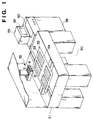
- Fig. 1 is a perspective view showing a structure of a color-filter manufacturing apparatus according to an embodiment of the present invention.
- reference numeral 51 denotes a platform; 52, an XY ⁇ stage provided on the platform 51; 53, a color-filter substrate set on the XY ⁇ stage 52; 54, a color filter formed on the color-filter substrate 53; 55, ink-jet heads respectively containing R (red), G (green) and B (blue) ink for coloring the color filter 54; 58, a controller for controlling the overall operation of a color-filter manufacturing apparatus 90; 59, a teaching pendant (personal computer) as a display unit of the controller 58; and 60, a keyboard as an operation panel of the teaching pendant 59.
- teaching pendant personal computer
- Fig. 2 is a block diagram showing the construction of the controller 58 for controlling operation of the color-filter manufacturing apparatus 90.
- the teaching pendant 59 serves as input-output means of the controller 58.
- Numeral 62 denotes a display unit which displays information such as progress of manufacture or abnormality of the ink-jet heads.
- the keyboard 60 serves as an operation panel for designating operation of the color-filter manufacturing apparatus 90 and the like.
- the controller 58 controls the overall operation of the color-filter manufacturing apparatus 90.
- Numeral 65 denotes an interface unit for data transfer between the teaching pendant 59; 66, a CPU which controls the color-filter manufacturing apparatus 90; 67, a ROM in which control programs for operating the CPU 66 are stored; 68, a RAM for storing production information and the like; 70, a discharge controller which controls ink discharge to the respective pixels of the color filter; 71, a stage controller which controls the operation of the XY ⁇ stage 52 of the color-filter manufacturing apparatus 90.
- the color-filter manufacturing apparatus 90 is connected to the controller 58, and operates in accordance with instructions from the controller 58.
- Fig. 3 is a perspective view showing the structure of the ink-jet head 55 used in the color-filter manufacturing apparatus 90.
- three ink-jet heads 55 are provided corresponding to R, G and B three colors. As these ink-jet heads 55 have the same structure, Fig. 3 only shows one of these ink-jet heads.
- the ink-jet head 55 has a heater board 104, as a substrate on which a plurality of heaters 102 for heating ink are formed, and a top plate 106 to be placed on the heater board 104.
- a plurality of discharge orifices 108 are formed on top plate 106, and the discharge orifices 108 are connected to ink channels 110.
- the respective ink channels 110 are separated from each other by partition walls 112.
- the ink channels 110 are commonly connected at their rear ends to a single ink chamber 114, to which ink is supplied via an ink-supply orifice 116. The ink is supplied from the ink chamber 114 to the respective ink channels 110.
- the heater board 104 and the top plate 106 are aligned and assembled such that the respective heaters 102 are positioned corresponding to the respective ink channels 110.
- Fig. 3 shows only two heaters 102, the heaters 102 one-to-one correspond to the ink channels 110.
- the drive pulse it is possible to control the drive pulse to be applied to the heaters 102 by, e.g., controlling electric power, so as to adjust the size of bubbles, more specifically to freely control the volume of ink discharged from the discharge orifices.
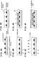
- Figs. 4A to 4F are explanatory views showing an example of color-filter manufacturing process. Next, the manufacture of the color filter 54 will be described with reference to Figs. 4A to 4F.
- a glass substrate is usually employed as the substrate 1, however, the substrate is not limited to glass, but any material can be used so far as it has necessary characteristics of a liquid-crystal color filter, such as transparency and mechanical strength.
- Fig. 4A shows the glass substrate 1 having a black matrix 2 constituting light-emitting portions 9 and light-shielding portions 10.
- resin material is applied onto the substrate 1 having the black matrix 2.
- the resin material itself is poor in ink receptivity, but can be inkphiled on certain condition(s) (for example, light emission or combination of light emission and heating) and it has a characteristic of setting on certain condition(s).
- prebaking is performed on the glass substrate 1 to form a resin layer 3 (Fig. 4B).
- the formation of the resin layer 3 is made by spin-coating, roll-coating, bar-coating, spray-coating, dip-coating or the like, and not limited to any particular method.
- the resin layer is partially inkphiled (Fig. 4C) by performing pattern-exposure on the resin layer on the light-transmitting portions 9 using a photomask 4, to form inkphiled portions 6 and uninkphiled portions 5 of the rein layer 3 (Fig. 4D).
- the ink-jet method includes a method utilizing thermal-energy and a method utilizing mechanical-energy. Any of these methods can be preferably used.
- any ink can be employed so far as it can be used for ink-jet printing.
- Coloring material of ink can be appropriately selected from various dyes or pigments in correspondence with transmission spectrum required for each of R, G and B pixels.
- the resin layer 3, colored and then light-emitted or light-emitted and heated, is set, and in accordance with necessity, a protective layer 8 is formed (Fig. 4F).
- This setting of the resin layer 3 is made by light emission or combination of light emission and heating, on condition(s) different from that of inkphiling of the resin layer, e.g., increased light exposure or heating at higher temperature.
- Figs. 5A to 5F are explanatory views showing another example of color-filter manufacturing process.
- Fig. 5A shows the glass substrate 1 having light-transmitting portions 7 and the black matrix 2 as light-shielding portion.
- resin material which can be set by light emission or combination of light emission and heating, and which has ink receptivity, is applied onto the substrate 1 on which the black matrix 2 is formed.
- pre-baking is performed, and a resin layer 3' is formed (Fig. 5B).
- the formation of the resin layer 3' can be made by spin-coating, roll-coating, bar-coating, spray-coating, dip-coating or the like, and not limited to any particular method.
- the part of the resin layer not covering the light-shielding black matrix 2 is masked with a photomask 4', and pattern-exposure is performed to set the other parts of the resin layer, to form uncolored portions 5' which are not ink-receptive (Fig. 5C).
- the coloring of R, G and B is made in one ink-discharge process by using the ink-jet head (Fig. 5D), and in accordance with necessity, the ink is dried.
- the photomask 4' used for pattern-exposure is a mask having an opening to set the portions light-shielded by the black matrix 2.
- the opening of the mask is preferably smaller than the width (light-shielding width) of the black matrix 2.
- both coloring matters and pigments can be used, further, both liquid ink and solid ink can be used.
- any resin material can be used so far as it has ink receptivity and it can be set by at least light emission or heating or combination thereof.
- resin such as acrylic resin, epoxy resin, silicon resin, cellulose derivatives or denatured materials such as hydroxypropylcellulose, hydroxyethylcellulose, methylcellulose and carboxymethylcellulose, can be used.
- Photo initiator can be employed to promote crosslinking reaction of the resin by light or light and heat.
- photo initiator bichromate, bisazide, radical initiators, cationic initiators, anionic initiators and the like can be used. Further, these photo initiators can be mixed or combined with other sensitizers.
- photooxide generator such as onium salt can be added as crosslinking agent. Note that to further promote crosslinking reaction, thermal processing can be performed after light emission.
- a resin layer containing the materials as mentioned above is excellent in thermal resistance and water resistance, and is fully resistible to high-temperature process or cleaning process in postprocessing.
- ink-jet method used in this embodiment a bubble-jet type method using electrothermal transducers as energy generators, or piezo-jet type method using piezoelectric devices can be employed.
- the coloring area and coloring pattern can be arbitrarily set.
- the present embodiment shows an example where a black matrix is formed on a substrate, however, the black matrix may be formed after a settable resin layer has been formed or after the resin has been colored.
- the formation of black matrix is preferably made by: forming a metal thin film by sputtering or vapor deposition; and patterning by a photolithography process. Note that any other method can be used to form the black matrix.
- Fig. 5E only light emission or only heating, or the combination thereof is used to set the settable resin material
- the protective layer 8 is formed (Fig. 5F).
- symbol h ⁇ represents light intensity.
- heat is applied instead of light h ⁇ .
- a second resin material of photo-setting type, thermosetting type or photo- and thermo-setting type is used as the protective layer 8.
- inorganic materials can be used for forming the protective layer 8 by sputtering or vapor deposition. Any material can be used to form the protective layer 8 so far as it has transparency as a color filter and sufficient resistance in subsequent ITO (Indium Tin Oxide) forming process, orientation film forming process and the like.
- ITO Indium Tin Oxide
- Figs. 6 and 7 are cross-sectional views showing the basic structure of a color LCD (Liquid Crystal Display) device 30 in which the above color filter is integrated.
- LCD Liquid Crystal Display
- the color LCD device 30 is constructed by assembling the color filter substrate 1 and an opposing substrate 21 and injecting liquid-crystal compound 18 between the substrates 1 and 21.
- a TFTs Thin Film Transistors
- a transparent pixel electrodes 20 are formed in matrix on the inner surface of the substrate 21.
- a color filter 54 is provided on the inner surface of the substrate 1, so that RGB color materials are arranged at positions respectively corresponding to the pixel electrodes 20.
- a transparent electrode (common electrode) 16 opposing to the pixel electrodes 20 is formed on all of the upper surface of the color filter 54.
- the black matrix 2 is formed on the color-filter substrate 1 side (see Fig.
- the black matrix 2 is formed on the opposing TFT substrate 21 side (see Fig. 7). Further, orientation films 19 are formed within the surfaces of both substrates. Liquid crystal molecules can be oriented in a specific direction by rubbing processing the orientation films 19. Polarizing plates 11 and 22 are attached to the outside of the respective glass substrates. The liquid-crystal compound 18 is filled in the gap (about 2 to 5 ⁇ m) between the glass substrates.
- the combination of a fluorescent light (not shown) and a scattering plate (not shown) is generally used.
- Display is made by using the liquid-crystal compound 18 as an optical shutter to change transmittance of the backlight.
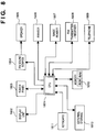
- Fig. 8 is a block diagram showing a construction of an information processing apparatus using the LCD device.
- the information processing apparatus functions as a word processor, a personal computer, a facsimile apparatus, and a copying machine.
- numeral 1801 denotes a controller which controls the overall apparatus. It comprises a CPU such as a microprocessor and various I/O ports, and it outputs control signals, data signals and the like to the respective elements, and inputs control signals and data signals from the respective elements for performing control.
- Numeral 1802 denotes a display unit which displays data such as various menus, document information, image data read by a image reader 1807, on a display screen.
- Numeral 1803 denotes a transparent pressure-sensitive type touch panel, provided on the display unit 1802. By pressing the surface of the touch panel 1803 with a finger or the like, an item, a coordinate position and the like can be inputted on the display unit 1802.
- Numeral 1804 denotes an FM (Frequency Modulation) sound source which accesses music information, generated by a music editor or the like and pre-stored in a memory 1810 or an external storage 1812 in the form of digital information, and performs frequency modulation on the read data.
- the electric signal from the FM sound source 1804 is converted into audio sound by a speaker 1805.
- a printer 1806 is used as an output terminal of a word processor, personal computer, facsimile apparatus or copying machine.
- the image reader 1807 photoelectrically reads an original and inputs the read data.
- the image reader 1807 is provided in the middle of original-conveying path for reading originals for facsimile transmission or copying or other various originals.
- Numeral 1808 denotes a facsimile (FAX) transmitter/receiver which performs facsimile transmission of original data, read by the image reader 1807, and receives facsimile signals and decodes the received facsimile signals.
- the FAX transmitter/receiver 1808 has an interface function between the information processing apparatus and an external device.
- Numeral 1809 denotes a telephone having various telephone functions such as ordinary telephone function, answering function and the like.
- Numeral 1811 denotes a keyboard for inputting document information, various commands and the like.
- the external storage 1812 comprises storage media such as a floppy disk and a hard disk, for storing document information, music or audio information, user's application programs and the like.
- Fig. 9 is a perspective view respectively showing the information processing apparatus having the construction in Fig. 8.
- numeral 1901 denotes a flat-panel display utilizing the above-described LCD device, for displaying various menus, figure information, document information and the like.
- the touch panel 1803 is used for inputting coordinates and designating items by pressing its surface with a finger or the like.
- Numeral 1902 denotes a handset used when the apparatus functions as a telephone.
- a keyboard 1903 is detachably connected to the apparatus main body via a cord, for inputting various document functions and various data.
- the keyboard 1903 has function keys 1904 for various functions.
- Numeral 1905 denotes a slot for inserting a floppy disk for the external storage 1812.
- Numeral 1906 denotes a paper feeder on which originals to be read by the image reader 1807 are set. The read originals are discharged from the rear portion of the apparatus. Upon facsimile reception and the like, read original data are print-outputted from an ink-jet printer 1907.
- this information processing apparatus functions as a personal computer or a word processor
- various information inputted from the keyboard 1811 is respectively processed by the controller 1801 in accordance with a predetermined program, and outputted as an image from the printer 1806.
- facsimile information inputted from the FAX transmitter/receiver 1808 via a communication line is reception-processed by the controller 1801 in accordance with a predetermined program, and outputted as a received image from the printer 1806.
- the information processing apparatus functions as a copying machine
- an original is read by the image reader 1807, and the read original data is outputted as a copied image from the printer 1806 via the controller 1801.
- the apparatus functions as the receiver of the facsimile apparatus
- the original data read by the image reader 1807 is transmission-processed by the controller 1801 in accordance with a predetermined program, and transmitted onto the communication line via the FAX transmitter/receiver 1808.
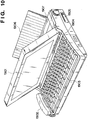
- the ink-jet printer can be integrated into the above information processing apparatus as shown in Fig. 10. This further improves portability.
- Fig. 10 the elements having the same functions as those in Fig. 9 have the same reference numerals.
- the glass substrate 53 is set on the XY ⁇ stage 52 of the color-filter manufacturing apparatus 90. After appropriate positioning, a color-filter forming area (coloring area) of the glass substrate 53 is moved to a position directly below the ink-jet head 55, then coloring of the pixels of the color filter is performed.
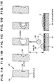
- Figs. 11A to 11E show ink-discharge operation characteristic of the present embodiment.
- one pixel of the color filter is colored with a plurality of discharge ink.
- at least ink I1 has already been discharged onto one pixel.
- At least a part of the already-applied ink I1 exists in liquid state before the ink I1 is completely absorbed into the resin layer 3 or completely dry, the next ink (I2) is discharged in the following manner, so that the next ink can mix with the already-applied ink within the same pixel area. This improves ink-application precision.
- a drive pulse is supplied to the heater 102 from the state shown in Fig. 11A, then a bubble occurs around the heater 102 as shown in Fig. 11B.
- the bubble grows as shown in Fig. 11C, then the ink I2 is discharged from the discharge nozzle.
- the distance A between the surface of ink-jet head 55 and the surface of the glass substrate 53 is set to a minimum distance such that the ink I2 is not separated from the ink-jet head 55 in the form of ink droplet. That is, as shown in Fig. 11C, the ink I2 does not become an ink droplet but a pillar and is applied onto the glass substrate 53.
- ink arrives at a desired pixel in the form of pillar before it is separated from the discharge nozzle. This greatly improves ink-arrival precision.
- the ink I2 comes into contact with the ink I1 that has already been discharged and exists in liquid state, and they mix with each other by surface tension. More specifically, when the ink I2 mixes with the ink I1, the ink I2 is drawn toward the ink I1 by the surface tension of the ink I1. Even if the ink I2 has been shifted from its discharge direction and not discharged in an exact direction, before the ink I2 reaches the glass substrate 53, the discharge direction of the ink I2 is corrected toward the ink I1 by the surface tension of the ink I1. As a result, the ink-application precision of the ink I2 can be improved. As shown in Fig.
- the currently-applied ink mixes with previously-applied ink, and as the currently-applied ink is drawn by the previously-applied ink, the currently-applied ink returns to a desired position within a pixel (the inkphiled portion 6).
- the peripheral pixels are not spattered with the ink.
- undesirable minute ink droplets other than the ink to be applied to the pixel can be prevented, the problem that the other pixels might be spotted with the slight ink droplets can be reduced.
- the application of ink in the form of pillar reduces spots on pixels other than a target pixel.
- the initially-applied ink I1 spreads to have a diameter of about 70 ⁇ m immediately after it has been applied onto the glass substrate. If the distance between a central point a1 of the ink I1 and a central point a2 of the ink I2 is 45 ⁇ m or less, or more preferably 20 to 30 ⁇ m, the ink I1 and the ink I2 mix with each other by surface tension. Note that the ink used in this example is in liquid state at 5°C, however, solid ink can be used so far as it spreads immediately after it has applied onto the substrate.
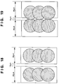
- the advantage in the above case where the mixture of the ink I2 with the previously-applied ink I1 in liquid state will be described. That is, as shown in Fig. 15A, if the ink I2 is discharged after the initial ink I1 has completely absorbed into the resin layer 3 or completely dried, the color of an ink-overlap portion B is deeper than that of a portion A, thus causing density unevenness. Further, the colored portion after the ink has dried is gourd-shaped as shown in Fig. 15B, which may cause uncolored portion(s). On the other hand, if the ink I2 is mixed with the ink I1 while at least a part of the ink I1 is in liquid state, the pixel can be colored with an even density as shown in Fig. 16A. Also, the shape of the colored portion after the ink has dried is oblong as shown in Fig. 16B, which prevents occurrence of uncolored portion(s).
- a drawing object is flexible material such as paper
- the ink-jet head cannot be moved close to the drawing objects within a certain range due to wrinkles and/or waving of the drawing object.
- it is required to maintain the interval between the drawing object and the ink-jet head about 0.9 to 1.5 mm.
- the ink discharge must be made at a predetermined speed (normally 10 m/s) or higher.
- the discharged ink becomes a plurality of ink droplets as shown in Figs. 17A and 17B.
- the scattered ink droplets are not discharged in uniform directions, which degrades ink-arrival precision. Further, as ink-discharge speeds of the respective ink droplets are different, when coloring is performed while the ink-jet head IJH is scanned with respect to the glass substrate 53, ink-arrival positions of the respective ink droplets are shifted.
- the drawing object is fixed-shaped material with a smooth surface such as glass substrate, the distance between the ink-jet head IJH and the surface of the glass substrate 53 can be reduced. This enables application of ink not in the form of ink droplet but in the form of pillar, onto the glass substrate 53, as shown in Figs. 17C to 17E.
- the smoothness (roughness) of the glass substrate to obtain the advantage of the present embodiment is set such that the distance from peaks to valleys in irregularities of the glass substrate surface is about 25 ⁇ m, or more preferably 20 ⁇ m or less.
- ink is discharged successively in the scanning direction of the ink-jet head, however, it can be arranged such that ink is applied to every other pixel in the first scanning, and in the second scanning, the ink is applied so as to fill gaps between the ink-applied pixels, while the initially-applied ink is in liquid state.
- the ink discharge is observed by using a microscope 202.
- the microscope 202 has a strobe 204 as a light source for observation.
- a driver 206 for the strobe 204 has a synchronizing circuit which inputs an external signal and drive the strobe 204 to emit light in synchronization with the external signal, and a delay circuit for shifting light emission timing from the timing of the external signal.
- an ink-jet head drive signal from an ink-jet driver 208 is used as the external signal.
- Figs. 21A to 21E are explanatory views showing the ink discharging process.
- strobe delay time is set to 0 ⁇ m and the strobe emits light in complete synchronization with the ink-jet head drive signal, it is found that the ink has not been discharged yet.
- the strobe delay time is set to 2 ⁇ m, it is found that the ink is just being discharged.
- the strobe delay time is set to 10 ⁇ m, it is found that the ink is in the form of pillar.
- the strobe delay time is increased, it can be observed that the ink state changes from the pillar into droplets.
- the ink state can be easily observed by setting the strobe light emission to be synchronized with the ink-jet head drive signal.
- a preferable ink-discharge speed is 5 m/s to 20 m/s.
- a preferable distance is 0.9 mm or less, or ore preferably 0.05 to 0.5 mm, or further preferably 0.05 to 0.2 mm.
- Fig. 22 shows the relation among the composition, the surface tension and the length of ink pillar. The level of surface tension of ink mainly depends on the content of cyclohexanol.
- Fig. 23 shows the relation between the content of cyclohexanol and surface tension.
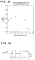
- Fig. 24 shows the relation between the surface tension when the ink-discharge amount is 80 ng and the length of ink pillar when the ink is discharged. As the surface tension is smaller, the length of ink pillar is longer.
- ink discharge has been performed under the conditions that the distance between the surface of the ink-jet head IJH and the glass substrate 53 is 0.1 mm, and the discharge speed is 8 m/s.
- a voltage pulse as shown in Fig. 25 is applied to the heaters 102.
- the ink-discharge speed can be controlled by changing the above voltage waveform.
- Fig. 26 shows the relation between a k-value which practically indicates the power to discharge ink and the ink-discharge speed. From this experimentally obtained relation between the k-value and the discharge speed, the pulse waveform of the voltage to be actually applied to the heaters 102 is set.
- k-value PWop/PWth
- Fig. 27 shows an example of the composition of ink available for color filters.
- solvents as shown in Fig. 28 can be used.
- these solvents more preferable solvents vapor upon heating of the heaters 102, at 250° C or lower, or more preferably at 230° C or lower.
- the content in the ink it is preferably 10 to 98 wt%, or more preferably 15 to 95 wt%.
- pigments organic pigments such as azo pigments and phthalocyanine pigments can be used.
- the pigments are inferior in color characteristics (transmittance, chromaticness contrast and the like), however, the pigments are superior in thermal resistance and optical resistance.
- the pigment is dispersed in an organic solvent using polymer compound or surfactant. After the dispersion, the particle diameter of the pigment is average 0.5 ⁇ m or less, or more preferably 0.2 ⁇ m or less.
- Preferable content of both dye and pigment in ink is 1 to 15 wt%, or more preferably 3 to 10 wt%.
- pH regulator As additives, pH regulator, antifungal agent, anti corrosive, viscosity regulator, surfactant, ultraviolet absorbent, photostabilizer (singlet oxygen quencher), chelating agent or the like can be added to ink in accordance with necessity.
- the content of additive in ink is 0.01 to 5 wt%, or more preferably 0.1 to 2.5 wt%.
- the present embodiment improves ink-arrival precision, and thus enables constant production of excellent color filters.
- the embodiment described above has exemplified a printer, which comprises means (e.g., an electrothermal transducer, laser beam generator, and the like) for generating heat energy as energy utilized upon execution of ink discharge, and causes a change in state of an ink by the heat energy, among the ink-jet printers.
- means e.g., an electrothermal transducer, laser beam generator, and the like
- heat energy as energy utilized upon execution of ink discharge
- causes a change in state of an ink by the heat energy among the ink-jet printers.
- the system is effective because, by applying at least one driving signal, which corresponds to printing information and gives a rapid temperature rise exceeding film boiling, to each of electrothermal transducers arranged in correspondence with a sheet or liquid channels holding a liquid (ink), heat energy is generated by the electrothermal transducer to effect film boiling on the heat acting surface of the print head, and consequently, a bubble can be formed in the liquid (ink) in one-to-one correspondence with the driving signal.
- the driving signal is applied as a pulse signal, the growth and shrinkage of the bubble can be attained instantly and adequately to achieve discharge of the liquid (ink) with the particularly high response characteristics.
- signals disclosed in U.S. Patent Nos. 4,463,359 and 4,345,262 are suitable. Note that further excellent printing can be performed by using the conditions described in U.S. Patent No. 4,313,124 of the invention which relates to the temperature rise rate of the heat acting surface.
- the arrangement using U.S. Patent Nos. 4,558,333 and 4,459,600 which disclose the arrangement having a heat acting portion arranged in a flexed region is also included in the present invention.
- the present invention can be effectively applied to an arrangement based on Japanese Patent Laid-Open No. 59-123670 which discloses the arrangement using a slot common to a plurality of electrothermal transducers as a discharge portion of the electrothermal transducers, or Japanese Patent Laid-Open No. 59-138461 which discloses the arrangement having an opening for absorbing a pressure wave of heat energy in correspondence with a discharge portion.
- a full line type print head having a length corresponding to the width of a maximum printing medium which can be printed by the printer, either the arrangement which satisfies the full-line length by combining a plurality of print heads as disclosed in the above specification or the arrangement as a single print head obtained by forming print heads integrally can be used.
- an exchangeable chip type print head which can be electrically connected to the apparatus main unit and can receive an ink from the apparatus main unit upon being mounted on the apparatus main unit or a cartridge type print head in which an ink tank is integrally arranged on the print head itself can be applicable to the present invention.
- recovery means for the print head, preliminary auxiliary means, and the like provided as an arrangement of the printer of the present invention since the printing operation can be further stabilized.
- examples of such means include, for the print head, capping means, cleaning means, pressurization or suction means, and preliminary heating means using electrothermal transducers, another heating element, or a combination thereof. It is also effective for stable printing to provide a preliminary discharge mode which performs discharge independently of printing.
- the ink is a liquid.
- the present invention may employ an ink which is solid at room temperature or less and softens or liquefies at room temperature, so far as the ink liquefies upon application of a use printing signal.
- an ink which is solid in a non-use state and liquefies upon heating may be used.
- an ink which liquefies upon application of heat energy according to a printing signal and is discharged in a liquid state, an ink which begins to solidify when it reaches a printing medium, or the like, is applicable to the present invention.
- an ink may be situated opposite electrothermal transducers while being held in a liquid or solid state in recess portions of a porous sheet or through holes, as described in Japanese Patent Laid-Open No. 54-56847 or 60-71260.
- the above-mentioned film boiling system is most effective for the above-mentioned inks.
- the present invention can improve ink-arrival precision by applying ink not in the form of ink droplet but in the form of pillar, thus enables manufacture of color filters with high precision.
- a color-filter manufacturing method which manufactures a color filter where occurrence of color mixture and colorless portion(s) are prevented while improving ink-arrival precision in applying ink onto a substrate.
- the method manufactures a color filter by discharging ink from an ink-jet head IJH on a substrate 53 so as to color respective pixels with a plurality of discharge ink.
- ink I2 discharged from the ink-jet head IJH is applied not in the form of ink droplet but in the form of pillar onto the substrate 53, the ink I2 is applied at a position within a pixel, where the ink I2 is to mix with previously-applied ink I1.
Landscapes
- Physics & Mathematics (AREA)
- Nonlinear Science (AREA)
- Mathematical Physics (AREA)
- Engineering & Computer Science (AREA)
- Chemical & Material Sciences (AREA)
- Crystallography & Structural Chemistry (AREA)
- Manufacturing & Machinery (AREA)
- General Physics & Mathematics (AREA)
- Optics & Photonics (AREA)
- Optical Filters (AREA)
- Liquid Crystal (AREA)
- Devices For Indicating Variable Information By Combining Individual Elements (AREA)
- Ink Jet (AREA)
Applications Claiming Priority (6)
| Application Number | Priority Date | Filing Date | Title |
|---|---|---|---|
| JP19523595 | 1995-07-31 | ||
| JP19523595 | 1995-07-31 | ||
| JP195235/95 | 1995-07-31 | ||
| JP18056496 | 1996-07-10 | ||
| JP180564/96 | 1996-07-10 | ||
| JP18056496A JP3124722B2 (ja) | 1995-07-31 | 1996-07-10 | カラーフィルタの製造方法及び製造装置及びカラーフィルタの区画された領域間の混色の低減方法及びカラーフィルタの区画された領域へのインク付与位置の精度向上方法及びカラーフィルタの区画された領域の着色ムラ低減方法 |
Publications (3)
| Publication Number | Publication Date |
|---|---|
| EP0756932A2 true EP0756932A2 (de) | 1997-02-05 |
| EP0756932A3 EP0756932A3 (de) | 1997-08-13 |
| EP0756932B1 EP0756932B1 (de) | 2001-11-07 |
Family
ID=26500044
Family Applications (1)
| Application Number | Title | Priority Date | Filing Date |
|---|---|---|---|
| EP96112360A Expired - Lifetime EP0756932B1 (de) | 1995-07-31 | 1996-07-31 | Verfahren zum Herstellen eines Farbfilters, Farbfilter, Anzeigevorrichtung und Apparat mit dieser Anzeigevorrichtung |
Country Status (7)
| Country | Link |
|---|---|
| US (1) | US6224205B1 (de) |
| EP (1) | EP0756932B1 (de) |
| JP (1) | JP3124722B2 (de) |
| KR (1) | KR100203009B1 (de) |
| CN (1) | CN1129024C (de) |
| AT (1) | ATE208274T1 (de) |
| DE (1) | DE69616685T2 (de) |
Cited By (15)
| Publication number | Priority date | Publication date | Assignee | Title |
|---|---|---|---|---|
| EP0790509A3 (de) * | 1996-02-16 | 1998-04-22 | Canon Kabushiki Kaisha | Herstellungsverfahren für ein Farbfilter und dafür geeignete Anordnung, Farbfilter, Anzeigevorrichtung und diese enthaltendes Gerät |
| EP0892028A3 (de) * | 1997-07-16 | 1999-02-03 | Seiko Epson Corporation | Zusammensetzung für organisches elektrolumineszentes Element und Verfahren zur Herstellung eines organischen elektrolumineszenten Elements |
| WO2001014915A1 (en) * | 1999-08-19 | 2001-03-01 | Matsushita Electric Industrial Co., Ltd. | Ink-jet head and method of manufacturing color filter |
| EP1093156A3 (de) * | 1999-10-13 | 2001-08-08 | Semiconductor Energy Laboratory Co., Ltd. | Vorrichtung zur Herstellung von Dünnfilmen |
| EP1072927A3 (de) * | 1999-07-29 | 2002-01-23 | Canon Kabushiki Kaisha | Farbfilter für eine Flüssigkristallanzeige und dazugehöriges Herstellungverfahren |
| EP1344649A2 (de) | 2002-03-13 | 2003-09-17 | Ricoh Company, Ltd. | Herstellung von einer Montageplatte für funktionelle Vorrichtung unter Verwendung eines Tintenstrahles |
| WO2004023574A1 (en) * | 2002-09-06 | 2004-03-18 | E.I. Du Pont De Nemours And Company | Methods for producing full-color organic electroluminescent devices |
| WO2004051350A1 (en) * | 2002-12-04 | 2004-06-17 | Skytech International Co., Ltd. | Micro-dispenser and method for manufacturing a color filter using the same |
| US6821553B2 (en) | 1996-11-25 | 2004-11-23 | Seiko Epson Corporation | Method of manufacturing organic EL element, organic EL element, and organic EL display device |
| US6872672B2 (en) | 1999-06-28 | 2005-03-29 | Semiconductor Energy Laboratory Co., Ltd. | Method of manufacturing an electro-optical device |
| US7067337B2 (en) | 1996-05-15 | 2006-06-27 | Seiko Epson Corporation | Thin film device provided with coating film, liquid crystal panel and electronic device, and method for making the thin film device |
| US7279194B2 (en) | 2000-02-04 | 2007-10-09 | Semiconductor Energy Laboratory Co., Ltd. | Thin film formation apparatus and method of manufacturing self-light-emitting device using thin film formation apparatus |
| WO2007145979A3 (en) * | 2006-06-05 | 2008-04-03 | Du Pont | Liquid composition for deposition of organic active materials in the field of oled printing |
| US7473928B1 (en) | 1999-10-12 | 2009-01-06 | Semiconductor Energy Laboratory Co., Ltd. | EL display device and a method of manufacturing the same |
| US8431182B2 (en) | 1996-09-19 | 2013-04-30 | Seiko Epson Corporation | Matrix type display device and manufacturing method thereof |
Families Citing this family (47)
| Publication number | Priority date | Publication date | Assignee | Title |
|---|---|---|---|---|
| DE19954366A1 (de) * | 1999-11-11 | 2001-05-17 | Basf Ag | Verfahren zur Beschriftung von Kunststoffoberflächen |
| EP1193513B1 (de) * | 2000-09-27 | 2008-12-03 | DIC Corporation | Verfahren zur Herstellung eines Farbfilters |
| US6872586B2 (en) | 2000-10-17 | 2005-03-29 | Seiko Epson Corporation | Method of manufacture of active matrix substrate and liquid crystal display device |
| JP4797246B2 (ja) * | 2001-01-05 | 2011-10-19 | 大日本印刷株式会社 | カラーフィルタ製造用の塗布装置 |
| AU2002234258A1 (en) * | 2001-01-22 | 2002-07-30 | Sun Microsystems, Inc. | Peer-to-peer network computing platform |
| JP2002365425A (ja) * | 2001-06-12 | 2002-12-18 | Rohm Co Ltd | カラー液晶表示装置およびその製造方法 |
| US7219970B2 (en) * | 2003-10-14 | 2007-05-22 | Hewlett-Packard Development Company, L.P. | Method and a system for single ligament fluid dispensing |
| US7011529B2 (en) * | 2004-03-01 | 2006-03-14 | Anritsu Company | Hermetic glass bead assembly having high frequency compensation |
| US20050255253A1 (en) * | 2004-05-13 | 2005-11-17 | White John M | Apparatus and methods for curing ink on a substrate using an electron beam |
| US20050253917A1 (en) * | 2004-05-13 | 2005-11-17 | Quanyuan Shang | Method for forming color filters in flat panel displays by inkjetting |
| JP2005331619A (ja) | 2004-05-18 | 2005-12-02 | Sharp Corp | パターン部材およびその製造方法 |
| JP4561226B2 (ja) * | 2004-08-06 | 2010-10-13 | セイコーエプソン株式会社 | カラーフィルタの成膜方法 |
| US20060092218A1 (en) * | 2004-11-04 | 2006-05-04 | Applied Materials, Inc. | Methods and apparatus for inkjet printing |
| US7413272B2 (en) * | 2004-11-04 | 2008-08-19 | Applied Materials, Inc. | Methods and apparatus for precision control of print head assemblies |
| US20060093751A1 (en) * | 2004-11-04 | 2006-05-04 | Applied Materials, Inc. | System and methods for inkjet printing for flat panel displays |
| US20070042113A1 (en) * | 2004-11-04 | 2007-02-22 | Applied Materials, Inc. | Methods and apparatus for inkjet printing color filters for displays using pattern data |
| US20060109296A1 (en) * | 2004-11-04 | 2006-05-25 | Bassam Shamoun | Methods and apparatus for inkjet printing color filters for displays |
| US7556334B2 (en) * | 2004-11-04 | 2009-07-07 | Applied Materials, Inc. | Methods and apparatus for aligning print heads |
| US7268006B2 (en) | 2004-12-30 | 2007-09-11 | E.I. Du Pont De Nemours And Company | Electronic device including a guest material within a layer and a process for forming the same |
| US20060159843A1 (en) * | 2005-01-18 | 2006-07-20 | Applied Materials, Inc. | Method of substrate treatment for manufacturing of color filters by inkjet printing systems |
| US20060185587A1 (en) * | 2005-02-18 | 2006-08-24 | Applied Materials, Inc. | Methods and apparatus for reducing ink conglomerates during inkjet printing for flat panel display manufacturing |
| US20070015847A1 (en) * | 2005-07-15 | 2007-01-18 | Applied Materials, Inc. | Red printing ink for color filter applications |
| US7460267B2 (en) * | 2005-07-15 | 2008-12-02 | Applied Materials, Inc. | Green printing ink for color filter applications |
| US7544723B2 (en) * | 2005-07-15 | 2009-06-09 | Applied Materials, Inc. | Blue printing ink for color filter applications |
| TWI318685B (en) * | 2005-07-28 | 2009-12-21 | Applied Materials Inc | Methods and apparatus for concurrent inkjet printing and defect inspection |
| US20070070132A1 (en) * | 2005-09-27 | 2007-03-29 | Fan-Cheung Sze | Inkjet delivery module |
| US20070070109A1 (en) * | 2005-09-29 | 2007-03-29 | White John M | Methods and systems for calibration of inkjet drop positioning |
| US20080018677A1 (en) * | 2005-09-29 | 2008-01-24 | White John M | Methods and apparatus for inkjet print head cleaning using an inflatable bladder |
| US7611217B2 (en) * | 2005-09-29 | 2009-11-03 | Applied Materials, Inc. | Methods and systems for inkjet drop positioning |
| US20070076040A1 (en) * | 2005-09-29 | 2007-04-05 | Applied Materials, Inc. | Methods and apparatus for inkjet nozzle calibration |
| US20070068560A1 (en) * | 2005-09-29 | 2007-03-29 | Quanyuan Shang | Methods and apparatus for inkjet print head cleaning |
| TWI328520B (en) * | 2006-02-07 | 2010-08-11 | Applied Materials Inc | Methods and apparatus for reducing irregularities in color filters |
| US20070210703A1 (en) * | 2006-02-28 | 2007-09-13 | Osram Opto Semiconductors Gmbh | Electroluminescent device and method for producing it |
| US20070252863A1 (en) * | 2006-04-29 | 2007-11-01 | Lizhong Sun | Methods and apparatus for maintaining inkjet print heads using parking structures with spray mechanisms |
| US20070256709A1 (en) * | 2006-04-29 | 2007-11-08 | Quanyuan Shang | Methods and apparatus for operating an inkjet printing system |
| US20070263026A1 (en) * | 2006-04-29 | 2007-11-15 | Quanyuan Shang | Methods and apparatus for maintaining inkjet print heads using parking structures |
| US7992956B2 (en) * | 2006-06-07 | 2011-08-09 | Applied Materials, Inc. | Systems and methods for calibrating inkjet print head nozzles using light transmittance measured through deposited ink |
| US20080024548A1 (en) * | 2006-07-26 | 2008-01-31 | Applied Materials, Inc. | Methods and apparatus for purging a substrate during inkjet printing |
| US20080024532A1 (en) * | 2006-07-26 | 2008-01-31 | Si-Kyoung Kim | Methods and apparatus for inkjet printing system maintenance |
| WO2008013902A2 (en) * | 2006-07-28 | 2008-01-31 | Applied Materials, Inc. | Methods and apparatus for improved manufacturing of color filters |
| US20080204501A1 (en) * | 2006-12-01 | 2008-08-28 | Shinichi Kurita | Inkjet print head pressure regulator |
| US7857413B2 (en) | 2007-03-01 | 2010-12-28 | Applied Materials, Inc. | Systems and methods for controlling and testing jetting stability in inkjet print heads |
| JP4858283B2 (ja) * | 2007-04-18 | 2012-01-18 | セイコーエプソン株式会社 | 流体噴射装置 |
| US7637587B2 (en) * | 2007-08-29 | 2009-12-29 | Applied Materials, Inc. | System and method for reliability testing and troubleshooting inkjet printers |
| WO2009076248A1 (en) * | 2007-12-06 | 2009-06-18 | Applied Materials, Inc. | Systems and methods for improving measurement of light transmittance through ink deposited on a substrate |
| KR20100110323A (ko) * | 2007-12-06 | 2010-10-12 | 어플라이드 머티어리얼스, 인코포레이티드 | 라인 스캔 카메라를 사용하여 기판 상의 픽셀 웰들에 증착된 잉크를 측정하기 위한 방법 및 장치 |
| US20090251504A1 (en) * | 2008-03-31 | 2009-10-08 | Applied Materials, Inc. | Systems and methods for wet in-situ calibration using measurement of light transmittance through ink deposited on a substrate |
Family Cites Families (24)
| Publication number | Priority date | Publication date | Assignee | Title |
|---|---|---|---|---|
| DE2361762C3 (de) * | 1973-12-12 | 1980-04-17 | Philips Patentverwaltung Gmbh, 2000 Hamburg | Schreib-Vorrichtung zum punktförmigen selektiven Übertragen flüssiger Farbe |
| CA1127227A (en) | 1977-10-03 | 1982-07-06 | Ichiro Endo | Liquid jet recording process and apparatus therefor |
| JPS5936879B2 (ja) | 1977-10-14 | 1984-09-06 | キヤノン株式会社 | 熱転写記録用媒体 |
| US4330787A (en) | 1978-10-31 | 1982-05-18 | Canon Kabushiki Kaisha | Liquid jet recording device |
| US4345262A (en) * | 1979-02-19 | 1982-08-17 | Canon Kabushiki Kaisha | Ink jet recording method |
| JPS5931944B2 (ja) | 1979-04-02 | 1984-08-06 | キヤノン株式会社 | 液体噴射記録法 |
| US4463359A (en) | 1979-04-02 | 1984-07-31 | Canon Kabushiki Kaisha | Droplet generating method and apparatus thereof |
| US4313124A (en) | 1979-05-18 | 1982-01-26 | Canon Kabushiki Kaisha | Liquid jet recording process and liquid jet recording head |
| US4558333A (en) | 1981-07-09 | 1985-12-10 | Canon Kabushiki Kaisha | Liquid jet recording head |
| JPS5975205A (ja) | 1982-10-25 | 1984-04-27 | Seiko Epson Corp | カラ−フイルタの製造方法 |
| JPS59123670A (ja) | 1982-12-28 | 1984-07-17 | Canon Inc | インクジエツトヘツド |
| JPS59138461A (ja) | 1983-01-28 | 1984-08-08 | Canon Inc | 液体噴射記録装置 |
| JPS6071260A (ja) | 1983-09-28 | 1985-04-23 | Erumu:Kk | 記録装置 |
| JPS61274949A (ja) | 1985-05-31 | 1986-12-05 | Canon Inc | 記録方式 |
| DE3620334A1 (de) | 1985-06-21 | 1987-01-02 | Sharp Kk | Druckverfahren |
| JPS6213357A (ja) | 1985-07-12 | 1987-01-22 | Tokyo Electric Co Ltd | インクジエツトプリンタ |
| JPS63235901A (ja) | 1987-03-24 | 1988-09-30 | Fujitsu Ltd | カラ−フイルタの形成方法 |
| JP2692833B2 (ja) | 1988-02-25 | 1997-12-17 | 株式会社東芝 | 液晶セルの製造方法 |
| US5285298A (en) | 1988-07-29 | 1994-02-08 | Canon Kabushiki Kaisha | Color display apparatus |
| JPH04129746A (ja) | 1990-09-21 | 1992-04-30 | Ricoh Co Ltd | 記録方法及び記録装置 |
| DE69333000T2 (de) * | 1992-06-01 | 2004-02-19 | Lg. Philips Lcd Co., Ltd. | Herstellungverfahren einer Flüssigkristallanzeige |
| JP3332515B2 (ja) | 1993-11-24 | 2002-10-07 | キヤノン株式会社 | カラーフィルタ、その製造方法及び液晶パネル |
| JP2839133B2 (ja) * | 1994-03-31 | 1998-12-16 | キヤノン株式会社 | カラーフィルタの製造方法及び製造装置及び液晶表示装置の製造方法及び液晶表示装置を備えた装置の製造方法 |
| JP2555986B2 (ja) * | 1994-06-23 | 1996-11-20 | 日本電気株式会社 | 高感度テレビカメラ装置 |
-
1996
- 1996-07-10 JP JP18056496A patent/JP3124722B2/ja not_active Expired - Fee Related
- 1996-07-29 US US08/687,985 patent/US6224205B1/en not_active Expired - Lifetime
- 1996-07-30 KR KR1019960031394A patent/KR100203009B1/ko not_active Expired - Fee Related
- 1996-07-31 DE DE69616685T patent/DE69616685T2/de not_active Expired - Lifetime
- 1996-07-31 EP EP96112360A patent/EP0756932B1/de not_active Expired - Lifetime
- 1996-07-31 CN CN96106995A patent/CN1129024C/zh not_active Expired - Fee Related
- 1996-07-31 AT AT96112360T patent/ATE208274T1/de not_active IP Right Cessation
Cited By (36)
| Publication number | Priority date | Publication date | Assignee | Title |
|---|---|---|---|---|
| US6500485B1 (en) | 1996-02-16 | 2002-12-31 | Canon Kabushiki Kaisha | Color filter manufacturing method and apparatus, color filter, display device, and apparatus having display device |
| EP0790509A3 (de) * | 1996-02-16 | 1998-04-22 | Canon Kabushiki Kaisha | Herstellungsverfahren für ein Farbfilter und dafür geeignete Anordnung, Farbfilter, Anzeigevorrichtung und diese enthaltendes Gerät |
| US7229859B2 (en) | 1996-05-15 | 2007-06-12 | Seiko Epson Corporation | Thin film device provided with coating film, liquid crystal panel and electronic device, and method for making the thin film device |
| US7067337B2 (en) | 1996-05-15 | 2006-06-27 | Seiko Epson Corporation | Thin film device provided with coating film, liquid crystal panel and electronic device, and method for making the thin film device |
| US8580333B2 (en) | 1996-09-19 | 2013-11-12 | Seiko Epson Corporation | Matrix type display device with optical material at predetermined positions and manufacturing method thereof |
| US8431182B2 (en) | 1996-09-19 | 2013-04-30 | Seiko Epson Corporation | Matrix type display device and manufacturing method thereof |
| US7662425B2 (en) | 1996-11-25 | 2010-02-16 | Seiko Epson Corporation | Method of manufacturing organic EL element, organic EL element and organic EL display device |
| US6821553B2 (en) | 1996-11-25 | 2004-11-23 | Seiko Epson Corporation | Method of manufacturing organic EL element, organic EL element, and organic EL display device |
| US6863961B2 (en) | 1996-11-25 | 2005-03-08 | Seiko Epson Corporation | Method of manufacturing organic EL element, organic EL element, and organic EL display device |
| US8614545B2 (en) | 1996-11-25 | 2013-12-24 | Seiko Epson Corporation | Organic EL display device having a bank formed to fill spaces between pixel electrodes |
| US6838192B2 (en) | 1996-11-25 | 2005-01-04 | Seiko Epson Corporation | Method of manufacturing organic EL element, organic EL element, and organic EL display device |
| EP0892028A3 (de) * | 1997-07-16 | 1999-02-03 | Seiko Epson Corporation | Zusammensetzung für organisches elektrolumineszentes Element und Verfahren zur Herstellung eines organischen elektrolumineszenten Elements |
| US6843937B1 (en) | 1997-07-16 | 2005-01-18 | Seiko Epson Corporation | Composition for an organic EL element and method of manufacturing the organic EL element |
| US6872672B2 (en) | 1999-06-28 | 2005-03-29 | Semiconductor Energy Laboratory Co., Ltd. | Method of manufacturing an electro-optical device |
| EP1072927A3 (de) * | 1999-07-29 | 2002-01-23 | Canon Kabushiki Kaisha | Farbfilter für eine Flüssigkristallanzeige und dazugehöriges Herstellungverfahren |
| US6475683B1 (en) | 1999-07-29 | 2002-11-05 | Canon Kabushiki Kaisha | Color filter, process for producing it, and liquid crystal panel |
| KR100374272B1 (ko) * | 1999-07-29 | 2003-03-03 | 캐논 가부시끼가이샤 | 칼라 필터, 그의 제조 방법 및 액정 패널 |
| WO2001014915A1 (en) * | 1999-08-19 | 2001-03-01 | Matsushita Electric Industrial Co., Ltd. | Ink-jet head and method of manufacturing color filter |
| US8884301B2 (en) | 1999-10-12 | 2014-11-11 | Semiconductor Energy Laboratory Co., Ltd. | EL display device and a method of manufacturing the same |
| US8319224B2 (en) | 1999-10-12 | 2012-11-27 | Semiconductor Energy Laboratory Co., Ltd. | EL display device and a method of manufacturing the same |
| US8133748B2 (en) | 1999-10-12 | 2012-03-13 | Semiconductor Energy Laboratory Co., Ltd. | EL display device and method of manufacturing the same |
| US7473928B1 (en) | 1999-10-12 | 2009-01-06 | Semiconductor Energy Laboratory Co., Ltd. | EL display device and a method of manufacturing the same |
| US7919341B2 (en) | 1999-10-13 | 2011-04-05 | Semiconductor Energy Laboratory Co., Ltd. | Thin film forming apparatus |
| EP1093156A3 (de) * | 1999-10-13 | 2001-08-08 | Semiconductor Energy Laboratory Co., Ltd. | Vorrichtung zur Herstellung von Dünnfilmen |
| US7115434B2 (en) | 1999-10-13 | 2006-10-03 | Semiconductor Energy Laboratory Co., Ltd. | Method for precisely forming light emitting layers in a semiconductor device |
| US7279194B2 (en) | 2000-02-04 | 2007-10-09 | Semiconductor Energy Laboratory Co., Ltd. | Thin film formation apparatus and method of manufacturing self-light-emitting device using thin film formation apparatus |
| US8517530B2 (en) | 2002-03-13 | 2013-08-27 | Ricoh Company, Ltd. | Fabrication of functional device mounting board making use of inkjet technique |
| US7553375B2 (en) | 2002-03-13 | 2009-06-30 | Ricoh Company, Ltd. | Fabrication of functional device mounting board making use of inkjet technique |
| US6918666B2 (en) | 2002-03-13 | 2005-07-19 | Ricoh Company, Ltd. | Fabrication of functional device mounting board making use of inkjet technique |
| EP1344649A3 (de) * | 2002-03-13 | 2003-10-29 | Ricoh Company, Ltd. | Herstellung von einer Montageplatte für funktionelle Vorrichtung unter Verwendung eines Tintenstrahles |
| EP1344649A2 (de) | 2002-03-13 | 2003-09-17 | Ricoh Company, Ltd. | Herstellung von einer Montageplatte für funktionelle Vorrichtung unter Verwendung eines Tintenstrahles |
| US7226799B2 (en) | 2002-09-06 | 2007-06-05 | E. I. Du Pont De Nemours And Company | Methods for producing full-color organic electroluminescent devices |
| US7098060B2 (en) | 2002-09-06 | 2006-08-29 | E.I. Du Pont De Nemours And Company | Methods for producing full-color organic electroluminescent devices |
| WO2004023574A1 (en) * | 2002-09-06 | 2004-03-18 | E.I. Du Pont De Nemours And Company | Methods for producing full-color organic electroluminescent devices |
| WO2004051350A1 (en) * | 2002-12-04 | 2004-06-17 | Skytech International Co., Ltd. | Micro-dispenser and method for manufacturing a color filter using the same |
| WO2007145979A3 (en) * | 2006-06-05 | 2008-04-03 | Du Pont | Liquid composition for deposition of organic active materials in the field of oled printing |
Also Published As
| Publication number | Publication date |
|---|---|
| US6224205B1 (en) | 2001-05-01 |
| CN1129024C (zh) | 2003-11-26 |
| JP3124722B2 (ja) | 2001-01-15 |
| KR100203009B1 (ko) | 1999-06-15 |
| KR970005636A (ko) | 1997-02-19 |
| DE69616685T2 (de) | 2002-08-01 |
| DE69616685D1 (de) | 2001-12-13 |
| ATE208274T1 (de) | 2001-11-15 |
| EP0756932A3 (de) | 1997-08-13 |
| CN1170141A (zh) | 1998-01-14 |
| JPH09101411A (ja) | 1997-04-15 |
| EP0756932B1 (de) | 2001-11-07 |
Similar Documents
| Publication | Publication Date | Title |
|---|---|---|
| EP0756932B1 (de) | Verfahren zum Herstellen eines Farbfilters, Farbfilter, Anzeigevorrichtung und Apparat mit dieser Anzeigevorrichtung | |
| EP0675385B1 (de) | Verfahren und Vorrichtung zur Herstellung von Farbfiltern | |
| JP3697131B2 (ja) | カラーフィルタの製造方法、製造装置、カラーフィルタを備えた表示装置の製造方法及び該表示装置を備えた装置の製造方法 | |
| US6207948B1 (en) | Color filter, display device using color filter, apparatus comprising display device, ink-jet head, and color filter manufacturing method and apparatus | |
| US6604821B1 (en) | Method and apparatus for manufacturing color filter, display device using the color filter, and electronic equipment comprising the display device | |
| US6179400B1 (en) | Color filter manufacturing method and apparatus, color filter, display device, apparatus having display apparatus, and method of equalizing colored states of areas | |
| US6500485B1 (en) | Color filter manufacturing method and apparatus, color filter, display device, and apparatus having display device | |
| KR100255838B1 (ko) | 잉크 토출 밀도 설정 방법, 컬러 필터 제조 방법, 컬러 필터,표시 장치 및 표시 장치를 갖는 장치 | |
| KR20010083210A (ko) | 칼라 필터 제조 방법 및 장치 | |
| EP0702250B1 (de) | Herstellungsverfahren für Farbfilter, derart hergestellte Farbfilter, und Flüssigkristallanzeigetafel mit einem solchen Farbfilter | |
| JPH09300664A (ja) | カラーフィルタの製造方法及び製造装置及びカラーフィルタ及び表示装置及びこの表示装置を備えた装置及びプリント方法 | |
| JPH08271724A (ja) | カラーフィルタの製造装置及び製造方法及びカラーフィルタ及び液晶表示装置及びこの液晶表示装置を備えた装置 | |
| US6386700B1 (en) | Color-filter manufacturing method, color filter, display device, and apparatus having the display device | |
| JP3352335B2 (ja) | カラーフィルタの製造方法及び製造装置及びカラーフィルタ及び表示装置及びこの表示装置を備えた装置 | |
| JPH112711A (ja) | カラーフィルタの製造方法及びカラーフィルタ及び表示装置及びこの表示装置を備えた装置 | |
| JP3106104B2 (ja) | カラーフィルタの製造方法及び製造装置及びカラーフィルタ及び表示装置及びこの表示装置を備えた装置及び表示装置の製造方法 | |
| JPH1114820A (ja) | カラーフィルタの製造方法及び製造装置及びカラーフィルタ及び表示装置及びこの表示装置を備えた装置 | |
| JPH10250117A (ja) | カラーフィルタの製造装置及び製造方法及びカラーフィルタ及び表示装置及びこの表示装置を備えた装置 | |
| JPH1130713A (ja) | カラーフィルタの製造方法及び製造装置及びカラーフィルタ及び表示装置及びこの表示装置を備えた装置 | |
| JPH10253813A (ja) | カラーフィルタの製造方法及びカラーフィルタ及び表示装置及びこの表示装置を備えた装置 | |
| JP2006065343A (ja) | カラーフィルタの製造方法、表示パネルの製造方法、表示パネルを備えた情報処理装置の製造方法、液晶表示パネル、液晶表示パネルを備えた情報処装置、液晶表示パネルの製造方法、液晶表示パネルを備えた情報処理装置の製造方法 | |
| JP2006048080A (ja) | カラーフィルタの製造方法、表示パネルの製造方法、表示パネルを備えた情報処理装置の製造方法、液晶表示パネル、液晶表示パネルを備えた情報処装置、液晶表示パネルの製造方法、液晶表示パネルを備えた情報処理装置の製造方法 |
Legal Events
| Date | Code | Title | Description |
|---|---|---|---|
| PUAI | Public reference made under article 153(3) epc to a published international application that has entered the european phase |
Free format text: ORIGINAL CODE: 0009012 |
|
| AK | Designated contracting states |
Kind code of ref document: A2 Designated state(s): AT BE CH DE DK ES FI FR GB GR IE IT LI LU NL PT SE |
|
| PUAL | Search report despatched |
Free format text: ORIGINAL CODE: 0009013 |
|
| AK | Designated contracting states |
Kind code of ref document: A3 Designated state(s): AT BE CH DE DK ES FI FR GB GR IE IT LI LU NL PT SE |
|
| 17P | Request for examination filed |
Effective date: 19971230 |
|
| 17Q | First examination report despatched |
Effective date: 19990723 |
|
| GRAG | Despatch of communication of intention to grant |
Free format text: ORIGINAL CODE: EPIDOS AGRA |
|
| GRAG | Despatch of communication of intention to grant |
Free format text: ORIGINAL CODE: EPIDOS AGRA |
|
| GRAH | Despatch of communication of intention to grant a patent |
Free format text: ORIGINAL CODE: EPIDOS IGRA |
|
| GRAH | Despatch of communication of intention to grant a patent |
Free format text: ORIGINAL CODE: EPIDOS IGRA |
|
| GRAA | (expected) grant |
Free format text: ORIGINAL CODE: 0009210 |
|
| AK | Designated contracting states |
Kind code of ref document: B1 Designated state(s): AT BE CH DE DK ES FI FR GB GR IE IT LI LU NL PT SE |
|
| PG25 | Lapsed in a contracting state [announced via postgrant information from national office to epo] |
Ref country code: LI Free format text: LAPSE BECAUSE OF FAILURE TO SUBMIT A TRANSLATION OF THE DESCRIPTION OR TO PAY THE FEE WITHIN THE PRESCRIBED TIME-LIMIT Effective date: 20011107 Ref country code: GR Free format text: LAPSE BECAUSE OF FAILURE TO SUBMIT A TRANSLATION OF THE DESCRIPTION OR TO PAY THE FEE WITHIN THE PRESCRIBED TIME-LIMIT Effective date: 20011107 Ref country code: FI Free format text: LAPSE BECAUSE OF FAILURE TO SUBMIT A TRANSLATION OF THE DESCRIPTION OR TO PAY THE FEE WITHIN THE PRESCRIBED TIME-LIMIT Effective date: 20011107 Ref country code: CH Free format text: LAPSE BECAUSE OF FAILURE TO SUBMIT A TRANSLATION OF THE DESCRIPTION OR TO PAY THE FEE WITHIN THE PRESCRIBED TIME-LIMIT Effective date: 20011107 Ref country code: BE Free format text: LAPSE BECAUSE OF FAILURE TO SUBMIT A TRANSLATION OF THE DESCRIPTION OR TO PAY THE FEE WITHIN THE PRESCRIBED TIME-LIMIT Effective date: 20011107 Ref country code: AT Free format text: LAPSE BECAUSE OF FAILURE TO SUBMIT A TRANSLATION OF THE DESCRIPTION OR TO PAY THE FEE WITHIN THE PRESCRIBED TIME-LIMIT Effective date: 20011107 |
|
| REF | Corresponds to: |
Ref document number: 208274 Country of ref document: AT Date of ref document: 20011115 Kind code of ref document: T |
|
| REG | Reference to a national code |
Ref country code: CH Ref legal event code: EP |
|
| REG | Reference to a national code |
Ref country code: IE Ref legal event code: FG4D |
|
| REF | Corresponds to: |
Ref document number: 69616685 Country of ref document: DE Date of ref document: 20011213 |
|
| REG | Reference to a national code |
Ref country code: GB Ref legal event code: IF02 |
|
| PG25 | Lapsed in a contracting state [announced via postgrant information from national office to epo] |
Ref country code: SE Free format text: LAPSE BECAUSE OF FAILURE TO SUBMIT A TRANSLATION OF THE DESCRIPTION OR TO PAY THE FEE WITHIN THE PRESCRIBED TIME-LIMIT Effective date: 20020207 Ref country code: PT Free format text: LAPSE BECAUSE OF FAILURE TO SUBMIT A TRANSLATION OF THE DESCRIPTION OR TO PAY THE FEE WITHIN THE PRESCRIBED TIME-LIMIT Effective date: 20020207 Ref country code: DK Free format text: LAPSE BECAUSE OF FAILURE TO SUBMIT A TRANSLATION OF THE DESCRIPTION OR TO PAY THE FEE WITHIN THE PRESCRIBED TIME-LIMIT Effective date: 20020207 |
|
| ET | Fr: translation filed | ||
| REG | Reference to a national code |
Ref country code: CH Ref legal event code: PL |
|
| PG25 | Lapsed in a contracting state [announced via postgrant information from national office to epo] |
Ref country code: ES Free format text: LAPSE BECAUSE OF FAILURE TO SUBMIT A TRANSLATION OF THE DESCRIPTION OR TO PAY THE FEE WITHIN THE PRESCRIBED TIME-LIMIT Effective date: 20020530 |
|
| PG25 | Lapsed in a contracting state [announced via postgrant information from national office to epo] |
Ref country code: LU Free format text: LAPSE BECAUSE OF NON-PAYMENT OF DUE FEES Effective date: 20020731 Ref country code: IE Free format text: LAPSE BECAUSE OF NON-PAYMENT OF DUE FEES Effective date: 20020731 |
|
| PLBE | No opposition filed within time limit |
Free format text: ORIGINAL CODE: 0009261 |
|
| STAA | Information on the status of an ep patent application or granted ep patent |
Free format text: STATUS: NO OPPOSITION FILED WITHIN TIME LIMIT |
|
| 26N | No opposition filed | ||
| REG | Reference to a national code |
Ref country code: IE Ref legal event code: MM4A |
|
| PGFP | Annual fee paid to national office [announced via postgrant information from national office to epo] |
Ref country code: DE Payment date: 20140731 Year of fee payment: 19 Ref country code: NL Payment date: 20140630 Year of fee payment: 19 |
|
| PGFP | Annual fee paid to national office [announced via postgrant information from national office to epo] |
Ref country code: GB Payment date: 20140724 Year of fee payment: 19 Ref country code: FR Payment date: 20140728 Year of fee payment: 19 |
|
| PGFP | Annual fee paid to national office [announced via postgrant information from national office to epo] |
Ref country code: IT Payment date: 20140702 Year of fee payment: 19 |
|
| REG | Reference to a national code |
Ref country code: DE Ref legal event code: R119 Ref document number: 69616685 Country of ref document: DE |
|
| GBPC | Gb: european patent ceased through non-payment of renewal fee |
Effective date: 20150731 |
|
| REG | Reference to a national code |
Ref country code: NL Ref legal event code: MM Effective date: 20150801 |
|
| PG25 | Lapsed in a contracting state [announced via postgrant information from national office to epo] |
Ref country code: DE Free format text: LAPSE BECAUSE OF NON-PAYMENT OF DUE FEES Effective date: 20160202 Ref country code: GB Free format text: LAPSE BECAUSE OF NON-PAYMENT OF DUE FEES Effective date: 20150731 Ref country code: IT Free format text: LAPSE BECAUSE OF NON-PAYMENT OF DUE FEES Effective date: 20150731 |
|
| REG | Reference to a national code |
Ref country code: FR Ref legal event code: ST Effective date: 20160331 |
|
| PG25 | Lapsed in a contracting state [announced via postgrant information from national office to epo] |
Ref country code: FR Free format text: LAPSE BECAUSE OF NON-PAYMENT OF DUE FEES Effective date: 20150731 Ref country code: NL Free format text: LAPSE BECAUSE OF NON-PAYMENT OF DUE FEES Effective date: 20150801 |