EP0757497B1 - Appareil de conversion photoélectrique pour images en couleur - Google Patents
Appareil de conversion photoélectrique pour images en couleur Download PDFInfo
- Publication number
- EP0757497B1 EP0757497B1 EP96305670A EP96305670A EP0757497B1 EP 0757497 B1 EP0757497 B1 EP 0757497B1 EP 96305670 A EP96305670 A EP 96305670A EP 96305670 A EP96305670 A EP 96305670A EP 0757497 B1 EP0757497 B1 EP 0757497B1
- Authority
- EP
- European Patent Office
- Prior art keywords
- pixels
- row
- color filters
- rows
- output lines
- Prior art date
- Legal status (The legal status is an assumption and is not a legal conclusion. Google has not performed a legal analysis and makes no representation as to the accuracy of the status listed.)
- Expired - Lifetime
Links
- 238000006243 chemical reaction Methods 0.000 title claims description 20
- 239000003086 colorant Substances 0.000 claims description 16
- 230000000295 complement effect Effects 0.000 claims description 14
- 238000010586 diagram Methods 0.000 description 12
- 238000000034 method Methods 0.000 description 6
- 230000008859 change Effects 0.000 description 3
- 230000008569 process Effects 0.000 description 3
- 101100275473 Caenorhabditis elegans ctc-3 gene Proteins 0.000 description 2
- 101100168274 Neurospora crassa (strain ATCC 24698 / 74-OR23-1A / CBS 708.71 / DSM 1257 / FGSC 987) cox-3 gene Proteins 0.000 description 2
- 230000003213 activating effect Effects 0.000 description 2
- 230000006872 improvement Effects 0.000 description 2
- 230000002093 peripheral effect Effects 0.000 description 2
- 230000004044 response Effects 0.000 description 2
- 230000004913 activation Effects 0.000 description 1
- 238000007792 addition Methods 0.000 description 1
- 230000003321 amplification Effects 0.000 description 1
- 230000005540 biological transmission Effects 0.000 description 1
- 230000015572 biosynthetic process Effects 0.000 description 1
- 230000006866 deterioration Effects 0.000 description 1
- 230000000694 effects Effects 0.000 description 1
- 238000000605 extraction Methods 0.000 description 1
- 238000003199 nucleic acid amplification method Methods 0.000 description 1
- 230000003287 optical effect Effects 0.000 description 1
- 230000035945 sensitivity Effects 0.000 description 1
- 230000008054 signal transmission Effects 0.000 description 1
- 238000002834 transmittance Methods 0.000 description 1
- 230000004304 visual acuity Effects 0.000 description 1
Images





Classifications
-
- H—ELECTRICITY
- H04—ELECTRIC COMMUNICATION TECHNIQUE
- H04N—PICTORIAL COMMUNICATION, e.g. TELEVISION
- H04N25/00—Circuitry of solid-state image sensors [SSIS]; Control thereof
- H04N25/10—Circuitry of solid-state image sensors [SSIS]; Control thereof for transforming different wavelengths into image signals
- H04N25/11—Arrangement of colour filter arrays [CFA]; Filter mosaics
- H04N25/13—Arrangement of colour filter arrays [CFA]; Filter mosaics characterised by the spectral characteristics of the filter elements
- H04N25/135—Arrangement of colour filter arrays [CFA]; Filter mosaics characterised by the spectral characteristics of the filter elements based on four or more different wavelength filter elements
- H04N25/136—Arrangement of colour filter arrays [CFA]; Filter mosaics characterised by the spectral characteristics of the filter elements based on four or more different wavelength filter elements using complementary colours
-
- H—ELECTRICITY
- H04—ELECTRIC COMMUNICATION TECHNIQUE
- H04N—PICTORIAL COMMUNICATION, e.g. TELEVISION
- H04N25/00—Circuitry of solid-state image sensors [SSIS]; Control thereof
- H04N25/70—SSIS architectures; Circuits associated therewith
-
- H—ELECTRICITY
- H04—ELECTRIC COMMUNICATION TECHNIQUE
- H04N—PICTORIAL COMMUNICATION, e.g. TELEVISION
- H04N25/00—Circuitry of solid-state image sensors [SSIS]; Control thereof
- H04N25/10—Circuitry of solid-state image sensors [SSIS]; Control thereof for transforming different wavelengths into image signals
- H04N25/11—Arrangement of colour filter arrays [CFA]; Filter mosaics
- H04N25/13—Arrangement of colour filter arrays [CFA]; Filter mosaics characterised by the spectral characteristics of the filter elements
- H04N25/133—Arrangement of colour filter arrays [CFA]; Filter mosaics characterised by the spectral characteristics of the filter elements including elements passing panchromatic light, e.g. filters passing white light
-
- H—ELECTRICITY
- H04—ELECTRIC COMMUNICATION TECHNIQUE
- H04N—PICTORIAL COMMUNICATION, e.g. TELEVISION
- H04N25/00—Circuitry of solid-state image sensors [SSIS]; Control thereof
- H04N25/10—Circuitry of solid-state image sensors [SSIS]; Control thereof for transforming different wavelengths into image signals
- H04N25/11—Arrangement of colour filter arrays [CFA]; Filter mosaics
- H04N25/13—Arrangement of colour filter arrays [CFA]; Filter mosaics characterised by the spectral characteristics of the filter elements
- H04N25/135—Arrangement of colour filter arrays [CFA]; Filter mosaics characterised by the spectral characteristics of the filter elements based on four or more different wavelength filter elements
-
- H—ELECTRICITY
- H04—ELECTRIC COMMUNICATION TECHNIQUE
- H04N—PICTORIAL COMMUNICATION, e.g. TELEVISION
- H04N25/00—Circuitry of solid-state image sensors [SSIS]; Control thereof
- H04N25/70—SSIS architectures; Circuits associated therewith
- H04N25/76—Addressed sensors, e.g. MOS or CMOS sensors
-
- H—ELECTRICITY
- H04—ELECTRIC COMMUNICATION TECHNIQUE
- H04N—PICTORIAL COMMUNICATION, e.g. TELEVISION
- H04N9/00—Details of colour television systems
- H04N9/03—Circuitry for demodulating colour component signals modulated spatially by colour striped filters by frequency separation
Definitions
- the present invention relates to a photoelectric conversion apparatus composed for example of BASIS, MOT or SIT XY-addressable photoconverting elements and bearing color filters thereon.
- BASIS base stored image sensor
- Fig. 8 is an equivalent circuit diagram of a photoelectric conversion apparatus utilising BASIS as the color image sensor, wherein shown are a plurality of pixels 40 each comprising bipolar phototransistors 1 receiving photons at the base thereof; a resetting PMOS transistor 2; a control capacitance 3 (COX) for controlling the base potential; and an emitter output line 4.
- a plurality of pixels 40 each comprising bipolar phototransistors 1 receiving photons at the base thereof; a resetting PMOS transistor 2; a control capacitance 3 (COX) for controlling the base potential; and an emitter output line 4.
- vertical output lines 5; horizontal drive lines 6; and read-circuits 41 for reading odd and even vertical output-lines respectively, including: resetting MOS transistors 7 for the vertical output lines 5; transferring MOS transistors 8; accumulating capacitances 9 (CT) for accumulating the photo-induced charge of the bipolar phototransistors 1; transfer MOS transistors 10 to the horizontal output lines; horizontal output lines 11; resetting MOS transistors 12 for the horizontal output linesll; output amplifiers 13 for amplifying the signal of the horizontal output lines; horizontal scanning circuits 14 for scanning the signals transferred to the horizontal output line 11; and a vertical scanning circuit 15 for activating the horizontal drive lines 6.
- CT capacitances 9
- Such method is employed in the ordinary television scanning, as it is superior in the dynamic resolution, indicating the resolution when the object is moving, and in the S/N ratio (signal-to-noise ratio).
- the photoelectric conversion apparatus of the present invention is an apparatus of the kind such as disclosed in JP-A-63-186466 which comprises:
- the apparatus according to the present invention is intended to facilitate the extraction of same color signals, while employing a conventional arrangement of four colour filters.
- the photoelectric conversion apparatus of the present invention which is of the kind aforesaid, is characterised in that:
- Fig. 1 is a schematic circuit diagram of a first embodiment of the present invention, wherein shown are a bipolar phototransistor 1 for receiving photons at the base thereof; a resetting PMOS transistor 2; a control capacitance 3 (COX) for controlling the base potential; an emitter output line 4; a vertical output line 5; a horizontal drive line 6; a resetting NMOS transistor 7 for the vertical output line; a transfer NMOS transistor 8 for transferring the photon-induced charge; an accumulating capacitance 9 (CT) for temporarily accumulating the photon-induced charge; a transferring NMOS transistor 10 for transferring the charge of the accumulating capacitance CT 9; a horizontal output line 11; an NMOS transistor 12 for grounding the horizontal output line; an output amplifier 13; a horizontal scanning circuit 14; a vertical scanning circuit 15; an XY-addressable pixel 40 including the bipolar phototransistor 1, the resetting PMOS transistor 2 and the base potential controlling capacitance COX 3 mentioned
- a low-level pulse is supplied from the vertical scanning circuit 15 to the horizontal drive line 6-1 to render the PMOS transistors 2 of the pixels 40-11 - 40-14 conductive, thereby resetting the bases of the phototransistors 1 of this drive line to the ground level.
- a control pulse ⁇ VC is shifted to a high level to reset the vertical output lines.
- a control pulse ⁇ HR is shifted to a high level to reset the horizontal output line 11.
- photoinduced charges corresponding to the object image are accumulated in the bases of the phototransistors 1.
- a high level pulse is supplied to the horizontal drive line 6-1 to elevate the potentials of the bases of the phototransistors 1 through the control capacitances COX 3 connected to the horizontal drive line 6-1, thereby activating the phototransistors 1 and outputting the photoinduced charges to the emitters thereof.
- a control pulse ⁇ T1 is shifted to a high level to render the transfer NMOS transistors 8 conductive, thereby accumulating the photo-induced charges in the accumulating capacitances CT.
- a control pulse ⁇ T2 is shifted to a high level to render the transfer NMOS transistors 8 conductive, thereby accumulating the photoinduced charges in the accumulating capacitances CT.
- predetermined scanning pulses are supplied from the horizontal scanning circuit 14 to render the transfer NMOS transistors 10 conductive, whereby the image signals are released from output terminals OUT1 - OUT4, through the horizontal output lines 11 and after amplification to a predetermined level by the output by the output amplifiers 13.
- the control pulses ⁇ VC, ⁇ T1, ⁇ T2, ⁇ HR and the pulses from the horizontal scanning circuit 14 are similarly supplied also to an upper readout circuit shown in Fig. 1.
- the pixels are of mutually same characteristics, but are provided thereon with color filters of complementary colors as illustrated.
- the photoinduced charge of the pixel 40-11 (Cy) is transferred to the lower accumulating capacitance 9-11.
- the photoinduced charge of the pixel 40-12 (Ye) is transferred to the upper accumulating capacitance 9-12
- that of the pixel 40-13 (Cy) is transferred to the lower accumulating capacitance 9-13
- that of the pixel 40-14 (Ye) is transferred to the upper accumulating capacitance 9-14.
- the photoinduced charge of the pixel 40-21 (Mg) is transferred to the lower accumulating capacitance 9-21, that of the pixel 40-22 (G) is transferred to the upper accumulating capacitance 9-22, and that of the pixel 40-23 (Mg) is transferred to the lower accumulating capacitance 9-23.
- the photo-induced charges are transferred in succession to the accumulating capacitances, and, in response to the scanning pulses from the horizontal scanning circuit 14, the amplified photoinduced charges of the pixels 40-11 (Cy), 40-21 (Mg), 40-12 (Ye) and 40-22 (G) are respectively released from the output terminals OUT3, OUT4, OUT1 and OUT2.
- the output terminal OUT3 provides the Cy component of the amplified photoinduced charge
- the output terminals OUT4, OUT1 and OUT2 respectively provide the Mg, Ye and G components.
- the G pixel signals are released from the vertical output lines 5-0, 5-2,... Also the G and Ye pixel signals are obtained from the upper readout circuit 41. Consequently the Mg and G components of the photoinduced charges are respectively obtained from the output terminals OUT4 and OUT2, as explained above.
- the pixels are provided thereon with on-chip filters of complementary colors for XY addressing, in a mosaic array in the unit of 4 lines and 4 columns.
- Such complementary mosaic filters are formed on a wafer in the formation of the photoelectric conversion apparatuses, and each chip of the photoelectric conversion apparatus is divided afterwards from such wafer.
- the mosaic filters consist of cyan (Cy), yellow (Ye), magenta (Mg) and green (G) elements.
- Each line is composed of a repeating pattern of cyan (Cy) and yellow (Ye) elements or of magenta (Mg) and green (G) elements.
- the first and third lines consisting of the cyan (Cy) and yellow (Ye) elements are of a same layout
- the second and fourth lines consisting of the magenta (Mg) and green (G) elements
- Mg magenta
- G green
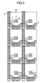
- Fig. 3 is a plan view of the pixel area of an area sensor embodying the present invention.
- the actual area sensor in composed of several ten thousand to several million pixels, by repeating the illustrated unit of 8 pixels in the horizontal and vertical directions.
- a base 16 of an npn phototransistor there are shown a base 16 of an npn phototransistor, an emitter 17 thereof, and a contact 18 between the emitter and the output line.
- an emitter output line 4 of the phototransistor 1 There are also shown, as shown in Fig. 1, an emitter output line 4 of the phototransistor 1, a vertical output line 5, and a horizontal drive line 6.
- the present embodiment is featured by a fact that in each column the output lines 4 of the pixels 40-41, 40-42, 40-43, and 40-44 of each fourth row are connected to respectively adjacent vertical output lines 5-0 to 5-3 at the other side of each pixel instead of the vertical output lines 5-1 to 5-4.
- the G output of each second row pixel and the Mg output of each fourth row pixel are connected to a same vertical output line, but, in the present embodiment, in each column the G pixels of each of the second and fourth row pixels are connected to the same vertical output line, so that each output terminal can always provide a signal of a same color in an all-pixel independent readout drive.
- each of the output terminals OUT1 - OUT4 always provides a signal of a same color, as shown in the following: Horizontal syncronization period 1H 2H 3H 4H 5H OUT1 Ye ⁇ Ye ⁇ Ye ⁇ Ye ⁇ Ye ⁇ OUT2 G ⁇ G ⁇ G ⁇ G ⁇ G OUT3 Cy ⁇ Cy ⁇ Cy ⁇ Cy ⁇ OUT4 Mg ⁇ Mg ⁇ Mg ⁇ Mg ⁇ Mg ⁇
- the present embodiment allows to provide a signal of a same color from each of the output terminals, while maintaining the arrangement of the complementary mosaic color filters in the visually optimum state, thereby enabling to simplify the signal processing circuit without any deterioration in the S/N ratio and in the dynamic resolution. Also the precision of automatic white balancing can be improved, as the arrangement of the complementary color mosaic filters is maintained as explained above.
- the ordered arrangements of the colour filters of the second and fourth rows are reversed with respect to each other, and in each column the pixels of the first, second and third rows are connected to one of the vertical output lines adjacent to that column, and the pixels of the fourth rows are connected to the other of the vertical output lines adjacent to the same column.
- the arrangement may be one in which in each column the pixels of the first, third and fourth rows are connected to one of the vertical output lines adjacent to that column, whilst the pixels of the second rows are connected to the other of the vertical output-lines adjacent to the same column.
- Fig. 4 is a schematic equivalent circuit diagram of a second embodiment of the present invention.
- the green (G) filters are replaced by white (W) filters, for achieving an improvement in the sensitivity, based on the difference in the optical transmittance.
- the W and Mg filters are displaced by a half cycle, and the emitter output lines of the pixels corresponding to such displaced filters are connected to the respectively adjacent output lines.
- the signal processing circuit can be simplified also in this embodiment.
- this embodiment allows to provide the image signal of a same color at each output terminal. Also the output terminal OUT2 provides a white signal, in addition to the complementary color signals of yellow, cyan and magenta, so that the transmission process becomes simple and effective for a color signal system in which the signal transmission is divided into an axis-I of orange-cyan color and an axis-Q of green-magenta color.
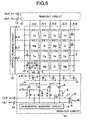
- Fig. 5 is a schematic equivalent circuit diagram of a third embodiment of the present invention, which is featured by a fact that the color filter arrangement in the first and second lines 6-1, 6-2 are displaced by a half cycle, or by a pixel, with respect to that of the third and fourth lines 6-3, 6-4.
- the above-explained mosaic arrangement of the color filters improves the color resolving power, thereby improving the resolution in comparison with the conventional configuration.
- the Ye and G pixels are respectively output from OUT1 and OUT2, through the vertical output lines 5-0, 5-2, ... and the upper readout circuit 41, while the Cy and Mg pixels are respectively output from OUT3 and OUT4, through the vertical output lines 5-1, 5-3, ... and the lower readout circuit 41. Since the Cy and Ye pixels, in addition to the Mg and G pixels, are displaced by one pixel from the basic pattern, there is achieved an improvement in the dynamic resolution, for the movement of the object. In this case, pattern layout of a complementary color mosaic filter on the pixel of the basic pattern is formed similarly to the pattern of the pixels 40.
- Fig. 6 is a circuit diagram of a fourth embodiment of the present invention, applied to a CMOS process compatible area sensor instead of the BASIS area sensor.
- Fig. 6 there are shown horizontal drive lines 21; vertical output lines 22; pixel output selection MOS switches 23; pixel output lines 24; and pixels 25.
- the pixels are provided thereon with complementary color mosaic filters, and the pixels 25-41, 25-42, ... connected to the horizontal drive line 21-4 are displaced, by a pixel, from those connected to the horizontal drive line 21-2.
- Fig. 7A is a circuit diagram of a pixel 25, wherein shown are a photoelectric conversion unit 26 composed of a photodiode; a photogate capacitance 27; a transfer NMOS transistor 28; a resetting NMOS transistor 29; and an amplifying NMOS transistor 30.
- the photoelectric conversion unit 26 is a depletion layer formed by the potential of the photogate capacitance 27, and the above-mentioned potential is controlled by a voltage controlling pulse 32 applied to the photogate capacitance 27.
- a control pulse 34 is shifted to a high level to render the resetting NMOS transistor 29 conductive, thereby resetting the gate of the amplifying NMOS transistor 30 to the power supply line 37.
- a control pulse 32 is shifted to a high level to activate the photoelectric conversion unit 26.
- a control pulse 33 is shifted to a high level state to render the transfer NMOS transistor 28 conductive, thereby transferring the photoinduced charge, accumulated in the photoelectric conversion unit 26 according to the amount of light received from the object image, to the gate of the amplifying NMOS transistor 30.
- the charge is amplified by the transistor 30 and released to the vertical output line 22, through the pixel output selection MOS switch 23 connected to the output line 38 and the pixel output line 24. Thereafter the image signals of the pixels are released by a scanning operation as in the readout circuit 41 shown in Fig. 1.
- the present embodiment enables, also in a sensor in which the pixel units and the peripheral circuits are formed by a same CMOS process, to effect outputs of constant colors independently for all the pixels, by displacing the pixel wirings of a line within the unit pixel pattern by a pixel, without any change in the original pattern of the complementary color mosaic filters. Also the output image signal, being amplified by a MOS transistor within the pixel, becomes a high level, thus providing a high S/N ratio.
- Fig. 7B is a circuit diagram showing the configuration of a fifth embodiment of the present invention, which is featured by a fact that the photogate 27 and the photoelectric conversion area 26, composed of a depletion layer, in the fourth embodiment are replaced by a PN photodiode 31. Also in this embodiment, the readout of all the pixels with constant colors can be achieved merely by a change in the wirings of the pixel output lines.
- a control pulse 36 is shifted to a high level state to render the resetting NMOS transistor 29 conductive, thereby resetting the gate of the amplifying NMOS transistor 30 to the power supply line 37.
- a photoinduced charge is generated in the PN photodiode 31, corresponding to the amount of light from the object image.
- a control pulse 35 is shifted to a high level state to render the transfer NMOS transistor 28 conductive, thereby transferring the photoinduced charge of the PN photodiode 31 to the gate of the amplifying NMOS transistor 30.
- the photoinduced charge is amplified by the transistor 30 and output to the vertical output line 22, through the pixel output selection MOS switch 23 connected to the output line 38 and the pixel output line 24. Thereafter the image signals of the pixels are output by a scanning operation as in the readout circuit 41 in Fig. 1.
- the described embodiments of the present invention all provide an-image signal of a same color from each of the output terminals even with complementary color mosaic filters designed for improving dynamic resolution and regardless of the driving method of the horizontal and vertical scanning circuits, thereby enabling simplification of the signal processing circuit to be used after the photoelectric conversion apparatus and to improve the precision of auto white balancing. Also the output signal of a same color can always be obtained at each of the output terminals, without any change in the filter arrangement, and the image signal of a high S/N ratio can be obtained by employing an amplifying transistor for the pixel output.
Landscapes
- Engineering & Computer Science (AREA)
- Multimedia (AREA)
- Signal Processing (AREA)
- Physics & Mathematics (AREA)
- Spectroscopy & Molecular Physics (AREA)
- Color Television Image Signal Generators (AREA)
- Transforming Light Signals Into Electric Signals (AREA)
- Solid State Image Pick-Up Elements (AREA)
- Facsimile Scanning Arrangements (AREA)
- Facsimile Heads (AREA)
Claims (11)
- Dispositif de conversion photoélectrique comportant :caractérisé en ce que :une pluralité de pixels (40:40-11 à 40-44) agencés de manière bidimensionnelle dans des directions verticale et horizontale,une pluralité de lignes de sortie verticales respectives (5:5 à 5-4) disposées adjacentes à des colonnes des pixels (40-11 à 40-41, 40-12 à 40-42, 40-13 à 40-43, 40-14 à 40-44) agencées dans la direction verticale,un premier circuit de lecture (41) agencé pour lire séquentiellement des signaux à partir de lignes impaires (5-1, 5-3) parmi ladite pluralité de lignes de sortie verticales, etun second circuit de lecture (41) agencé pour lire séquentiellement des signaux à partir de lignes paires (5-2, 5-4) parmi ladite pluralité de lignes de sortie verticales,des filtres colorés de quatre couleurs différentes A, B, C et D respectives pour ladite pluralité de pixels étant agencés selon un motif qui est répété toutes les quatre rangées de pixels agencées dans la direction horizontale, et motif où des filtres colorés respectifs de couleur A et des filtres colorés respectifs de couleur B sont agencés de manière alternée dans des premières rangées (40-11 à 40-14) et également dans des troisièmes rangées (40-31 à 40-34) des pixels agencés dans la direction horizontale, des filtres colorés respectifs de couleur C et des filtres colorés respectifs de couleur D étant agencés de manière alternée dans des deuxièmes rangées (40-21 à 40-24) et également dans des quatrièmes rangées (40-41 à 40-44) de pixels agencés dans la direction horizontale, et l'ordre d'agencement des filtres colorés dans au moins une desdites troisièmes et quatrièmes rangées, toutes les quatre rangées, est l'inverse de celui de l'ordre dans lesdites premières ou deuxièmes rangées,ladite pluralité de pixels (40) situés dans chaque colonne sont connectés auxdites lignes de sortie verticales (5), d'une manière telle que des pixels prédéterminés agencés dans la même colonne sont connectés à une première ligne parmi les lignes de sortie verticales (5-1, 5-2, 5-3, 5-4) adjacentes à ladite même colonne, et les pixels situés dans ladite même colonne autres que lesdits pixels prédéterminés sont connectés à l'autre ligne parmi les lignes de sortie verticales (5-0, 5-1, 5-2, 5-3) adjacentes à ladite même colonne, de sorte que ledit premier circuit de lecture (41) lit des signaux uniquement à partir de ces pixels au niveau desquels sont agencés les filtres colorés de couleurs A et C, et ledit second circuit de lecture (41) lit des signaux uniquement à partir de ces pixels au niveau desquels sont agencés les filtres colorés de couleurs B et D, respectivement.
- Dispositif selon la revendication 1, dans lequel chaque pixel (40) comporte un phototransistor bipolaire (1).
- Dispositif selon la revendication 1, dans lequel chaque pixel comporte un phototransistor MOS (28).
- Dispositif selon la revendication 1, dans lequel chaque pixel comporte une photodiode PN (31).
- Dispositif selon l'une quelconque des revendications précédentes, dans lequel lesdits filtres colorés sont des filtres mosaïques colorés complémentaires agencés selon un réseau unitaire se répétant, constitué de quatre rangées et de quatre colonnes.
- Dispositif selon l'une quelconque des revendications précédentes, dans lequel la couleur C ou D est le vert et les autres couleurs sont les couleurs complémentaires cyan, magenta et jaune.
- Dispositif selon la revendication 6, dans lequel les couleurs A, B, C et D sont respectivement le jaune, le cyan, le magenta et le vert.
- Dispositif selon l'une quelconque des revendications 1 à 5, dans lequel les couleurs A, B, C et D sont respectivement le jaune, le cyan, le magenta et le blanc.
- Dispositif selon l'une quelconque des revendications précédentes, dans lequel l'ordre d'agencement des filtres colorés dans chaque troisième rangée est le même que celui dans chaque première rangée, et l'ordre d'agencement des filtres colorés dans chaque quatrième rangée est l'inverse de celui dans chaque deuxième rangée, et
dans lequel, parmi les pixels agencés dans chaque même colonne, les pixels de chacune des première, deuxième et troisième rangées sont connectés à une première ligne parmi les lignes de sortie verticales adjacentes à ladite même colonne, et le pixel de chaque quatrième rangée est connecté à l'autre ligne parmi les lignes de sortie verticales adjacentes à ladite même colonne. - Dispositif de conversion photoélectrique selon l'une quelconque des revendications 1 à 8, dans lequel l'ordre d'agencement des filtres colorés dans chaque troisième rangée est le même que celui dans chaque première rangée, et l'ordre d'agencement des filtres colorés dans chaque quatrième rangée est l'inverse de celui dans chaque deuxième rangée, et
dans lequel, parmi les pixels agencés dans chaque même colonne, les pixels des première, troisième et quatrième rangées sont connectés à une des lignes de sortie verticales adjacentes à ladite même colonne, et le pixel de chaque deuxième rangée est connecté à l'autre ligne parmi les lignes de sortie verticales adjacentes à ladite même colonne. - Dispositif de conversion photoélectrique selon l'une quelconque des revendications 1 à 8, dans lequel l'ordre d'agencement des filtres colorés dans chaque troisième rangée est l'inverse de celui dans chaque première rangée, et l'ordre d'agencement des filtres colorés dans chaque quatrième rangée est l'inverse de celui dans chaque deuxième rangée, et
dans lequel, parmi les pixels agencés dans chaque même colonne, les pixels des première et deuxième rangées sont connectés à une des lignes de sortie verticales adjacentes à ladite même colonne, et les pixels des troisième et quatrième rangées sont connectés à l'autre ligne parmi les lignes de sortie verticales adjacentes à ladite même colonne.
Applications Claiming Priority (3)
| Application Number | Priority Date | Filing Date | Title |
|---|---|---|---|
| JP19747095A JP3432051B2 (ja) | 1995-08-02 | 1995-08-02 | 光電変換装置 |
| JP19747095 | 1995-08-02 | ||
| JP197470/95 | 1995-08-02 |
Publications (3)
| Publication Number | Publication Date |
|---|---|
| EP0757497A2 EP0757497A2 (fr) | 1997-02-05 |
| EP0757497A3 EP0757497A3 (fr) | 1998-04-08 |
| EP0757497B1 true EP0757497B1 (fr) | 2003-07-02 |
Family
ID=16375028
Family Applications (1)
| Application Number | Title | Priority Date | Filing Date |
|---|---|---|---|
| EP96305670A Expired - Lifetime EP0757497B1 (fr) | 1995-08-02 | 1996-07-31 | Appareil de conversion photoélectrique pour images en couleur |
Country Status (5)
| Country | Link |
|---|---|
| US (1) | US5786588A (fr) |
| EP (1) | EP0757497B1 (fr) |
| JP (1) | JP3432051B2 (fr) |
| DE (1) | DE69628886T2 (fr) |
| ES (1) | ES2199273T3 (fr) |
Families Citing this family (40)
| Publication number | Priority date | Publication date | Assignee | Title |
|---|---|---|---|---|
| JP3385760B2 (ja) * | 1994-02-21 | 2003-03-10 | ソニー株式会社 | 固体撮像装置及びその駆動方法 |
| US6035077A (en) * | 1996-05-03 | 2000-03-07 | Omnivision Technologies, Inc. | Single-chip color CMOS image sensor with two or more line reading structure and high-sensitivity interlace color structure |
| US6289139B1 (en) | 1996-05-03 | 2001-09-11 | Omnivision Technologies, Inc. | Single chip color CMOS image sensor with two or more line reading structure |
| JP3617887B2 (ja) * | 1996-10-14 | 2005-02-09 | シャープ株式会社 | 撮像装置 |
| DE59709654D1 (de) * | 1996-10-31 | 2003-04-30 | Stuttgart Mikroelektronik | Lichtempfindliche sensoreinheit für eine elektronische kamera, mit einer flächigen anordnung von bildpunkten sowie verfahren zum auslesen der bildpunkte zur farbsignalverarbeitung |
| JPH11103418A (ja) * | 1997-09-29 | 1999-04-13 | Canon Inc | 光電変換装置 |
| JP3548410B2 (ja) * | 1997-12-25 | 2004-07-28 | キヤノン株式会社 | 固体撮像装置および固体撮像装置の信号読み出し方法 |
| US6330029B1 (en) * | 1998-03-17 | 2001-12-11 | Eastman Kodak Company | Particular pattern of pixels for a color filter array which is used to derive luminance and chrominance values |
| US6466265B1 (en) * | 1998-06-22 | 2002-10-15 | Eastman Kodak Company | Parallel output architectures for CMOS active pixel sensors |
| US6570615B1 (en) | 1998-07-14 | 2003-05-27 | Analog Devices, Inc. | Pixel readout scheme for image sensors |
| US6512546B1 (en) * | 1998-07-17 | 2003-01-28 | Analog Devices, Inc. | Image sensor using multiple array readout lines |
| JP2000078473A (ja) | 1998-08-31 | 2000-03-14 | Canon Inc | 光電変換装置 |
| US6714243B1 (en) | 1999-03-22 | 2004-03-30 | Biomorphic Vlsi, Inc. | Color filter pattern |
| US6707496B1 (en) | 1999-09-15 | 2004-03-16 | Omnivision Technologies, Inc. | CMOS sensor having analog delay line for image processing |
| JP3467013B2 (ja) | 1999-12-06 | 2003-11-17 | キヤノン株式会社 | 固体撮像装置 |
| US6995800B2 (en) | 2000-01-27 | 2006-02-07 | Canon Kabushiki Kaisha | Image pickup apparatus utilizing a plurality of converging lenses |
| JP4011818B2 (ja) * | 2000-02-29 | 2007-11-21 | キヤノン株式会社 | 半導体固体撮像装置 |
| US6960817B2 (en) | 2000-04-21 | 2005-11-01 | Canon Kabushiki Kaisha | Solid-state imaging device |
| JP3750502B2 (ja) * | 2000-08-03 | 2006-03-01 | ソニー株式会社 | 固体撮像装置およびカメラシステム |
| JP2002252338A (ja) * | 2000-12-18 | 2002-09-06 | Canon Inc | 撮像装置及び撮像システム |
| JP4086514B2 (ja) * | 2002-02-13 | 2008-05-14 | キヤノン株式会社 | 光電変換装置及び撮像装置 |
| JP3833125B2 (ja) | 2002-03-01 | 2006-10-11 | キヤノン株式会社 | 撮像装置 |
| US7742088B2 (en) * | 2002-11-19 | 2010-06-22 | Fujifilm Corporation | Image sensor and digital camera |
| CN1518343A (zh) * | 2003-01-10 | 2004-08-04 | ���µ�����ҵ��ʽ���� | 固态成像装置和使用该装置的摄像机 |
| US7859581B2 (en) * | 2003-07-15 | 2010-12-28 | Eastman Kodak Company | Image sensor with charge binning and dual channel readout |
| JP3951994B2 (ja) * | 2003-09-16 | 2007-08-01 | ソニー株式会社 | 固体撮像装置およびカメラシステム |
| JP4553612B2 (ja) * | 2004-03-18 | 2010-09-29 | ルネサスエレクトロニクス株式会社 | 撮像素子およびそれを備えた撮像装置 |
| JP4385844B2 (ja) | 2004-04-23 | 2009-12-16 | ソニー株式会社 | 固体撮像装置および固体撮像装置の駆動方法 |
| JP2006295620A (ja) | 2005-04-12 | 2006-10-26 | Pentax Corp | 固体撮像素子 |
| US7465934B2 (en) | 2005-09-30 | 2008-12-16 | Eastman Kodak Company | Pixel array output routing structure for multi-channel CMOS imager sensors |
| JP4983093B2 (ja) * | 2006-05-15 | 2012-07-25 | ソニー株式会社 | 撮像装置および方法 |
| WO2009017184A1 (fr) * | 2007-08-01 | 2009-02-05 | Sharp Kabushiki Kaisha | Élément d'imagerie couleur, dispositif d'imagerie utilisant celui-ci et filtre |
| JP4367963B2 (ja) * | 2007-10-24 | 2009-11-18 | キヤノン株式会社 | 撮像装置、撮像システム、及び撮像装置の駆動方法 |
| US8081247B2 (en) * | 2008-06-18 | 2011-12-20 | Omnivision Technologies, Inc. | Partial row readout for image sensor |
| KR101639382B1 (ko) * | 2008-08-27 | 2016-07-13 | 삼성전자주식회사 | 높은 동적 범위를 가지는 영상을 생성하는 장치 및 방법 |
| JP5109962B2 (ja) * | 2008-12-22 | 2012-12-26 | ソニー株式会社 | 固体撮像装置および電子機器 |
| JP5822544B2 (ja) * | 2011-06-08 | 2015-11-24 | キヤノン株式会社 | 撮像装置および撮像システム |
| DE102011120099B4 (de) | 2011-12-02 | 2024-05-29 | Arnold & Richter Cine Technik Gmbh & Co. Betriebs Kg | Bildsensor und Verfahren zum Auslesen eines Bildsensors |
| AU2015206515B2 (en) | 2014-01-15 | 2019-12-12 | The United States Of America, As Represented By The Secretary, Department Of Health And Human Services | Cartilage targeting agents and their use |
| KR102820466B1 (ko) * | 2019-12-13 | 2025-06-17 | 삼성전자주식회사 | 이미지 센서, 그것을 포함하는 이미지 장치 및 그것의 동작 방법 |
Family Cites Families (10)
| Publication number | Priority date | Publication date | Assignee | Title |
|---|---|---|---|---|
| US4437112A (en) * | 1980-02-15 | 1984-03-13 | Canon Kabushiki Kaisha | Solid-state color imaging apparatus |
| JPH084131B2 (ja) * | 1987-01-29 | 1996-01-17 | キヤノン株式会社 | 光電変換装置 |
| DE3856165T2 (de) * | 1987-01-29 | 1998-08-27 | Canon Kk | Photovoltaischer Wandler |
| EP0368614B1 (fr) * | 1988-11-09 | 1993-09-15 | Canon Kabushiki Kaisha | Appareil de traitement d'un signal de couleur |
| US5115302A (en) * | 1990-04-26 | 1992-05-19 | Sharp Kabushiki Kaisha | Solid state color imaging device |
| US5406332A (en) * | 1992-03-06 | 1995-04-11 | Canon Kabushiki Kaisha | Photoelectric converting device |
| EP0570204B1 (fr) * | 1992-05-13 | 1996-07-10 | Matsushita Electric Industrial Co., Ltd. | Dispositif capteur d'images à l'état solide utilisant un filtre à couleur matriciel |
| US5541648A (en) * | 1992-10-09 | 1996-07-30 | Canon Kabushiki Kaisha | Color image pickup apparatus having a plurality of color filters arranged in an offset sampling structure |
| JP3862298B2 (ja) * | 1994-12-22 | 2006-12-27 | キヤノン株式会社 | 光電変換装置 |
| JP3031606B2 (ja) * | 1995-08-02 | 2000-04-10 | キヤノン株式会社 | 固体撮像装置と画像撮像装置 |
-
1995
- 1995-08-02 JP JP19747095A patent/JP3432051B2/ja not_active Expired - Fee Related
-
1996
- 1996-07-31 ES ES96305670T patent/ES2199273T3/es not_active Expired - Lifetime
- 1996-07-31 EP EP96305670A patent/EP0757497B1/fr not_active Expired - Lifetime
- 1996-07-31 DE DE69628886T patent/DE69628886T2/de not_active Expired - Lifetime
- 1996-08-01 US US08/690,936 patent/US5786588A/en not_active Expired - Lifetime
Also Published As
| Publication number | Publication date |
|---|---|
| EP0757497A2 (fr) | 1997-02-05 |
| JP3432051B2 (ja) | 2003-07-28 |
| EP0757497A3 (fr) | 1998-04-08 |
| ES2199273T3 (es) | 2004-02-16 |
| JPH0946480A (ja) | 1997-02-14 |
| DE69628886T2 (de) | 2004-05-13 |
| US5786588A (en) | 1998-07-28 |
| DE69628886D1 (de) | 2003-08-07 |
Similar Documents
| Publication | Publication Date | Title |
|---|---|---|
| EP0757497B1 (fr) | Appareil de conversion photoélectrique pour images en couleur | |
| US6784928B1 (en) | Solid state image pickup device and signal reading method thereof | |
| KR100979197B1 (ko) | 고체촬상장치 | |
| KR100331995B1 (ko) | 촬상장치에서 복수의 화소에 의해 공유되는 각 회로의 화소내의배치 | |
| KR101204571B1 (ko) | 고체 촬상 장치, 고체 촬상 장치의 구동 방법 및 카메라 | |
| KR100678612B1 (ko) | 증폭형 고체 촬상 장치 | |
| US8023018B2 (en) | Drive method for solid-state imaging device, solid-state imaging device, and imaging apparatus | |
| US7489357B2 (en) | Solid-state image pickup element having improved resolution and signal to noise ratio and solid-state image pickup apparatus using the same | |
| US4641183A (en) | Image pick-up apparatus | |
| WO2004049731A1 (fr) | Appareil d'imagerie a semi-conducteurs et son procede de lecture de signaux | |
| EP0933950B1 (fr) | Appareil et procédé de prise de vues en couleurs | |
| US5883667A (en) | Solid-state image pick-up device eliminating smear image component from video signal through real time control | |
| JP3956875B2 (ja) | 固体撮像装置 | |
| US7355641B2 (en) | Solid state imaging device reading non-adjacent pixels of the same color | |
| JP4354862B2 (ja) | 光センサ装置及び伝達回路装置 | |
| JP2964354B2 (ja) | 固体撮像装置及びその駆動方法 | |
| KR100369359B1 (ko) | 이웃하는 픽셀 간의 칼라 데이터 분리할 수 있는 이미지센서 및 그를 위한 데이터 스캔 방법 | |
| JP2004236028A (ja) | 固体撮像装置、カメラおよびカメラシステム | |
| JPS61234188A (ja) | 固体撮像装置 | |
| JPH0734590B2 (ja) | カラー画像用固体撮像素子 | |
| JP2004221994A (ja) | 固体撮像装置、カメラおよびカメラシステム |
Legal Events
| Date | Code | Title | Description |
|---|---|---|---|
| PUAI | Public reference made under article 153(3) epc to a published international application that has entered the european phase |
Free format text: ORIGINAL CODE: 0009012 |
|
| AK | Designated contracting states |
Kind code of ref document: A2 Designated state(s): DE ES FR GB IT NL |
|
| PUAL | Search report despatched |
Free format text: ORIGINAL CODE: 0009013 |
|
| AK | Designated contracting states |
Kind code of ref document: A3 Designated state(s): DE ES FR GB IT NL |
|
| 17P | Request for examination filed |
Effective date: 19980820 |
|
| 17Q | First examination report despatched |
Effective date: 20010222 |
|
| GRAH | Despatch of communication of intention to grant a patent |
Free format text: ORIGINAL CODE: EPIDOS IGRA |
|
| GRAH | Despatch of communication of intention to grant a patent |
Free format text: ORIGINAL CODE: EPIDOS IGRA |
|
| GRAA | (expected) grant |
Free format text: ORIGINAL CODE: 0009210 |
|
| AK | Designated contracting states |
Designated state(s): DE ES FR GB IT NL |
|
| REG | Reference to a national code |
Ref country code: GB Ref legal event code: FG4D |
|
| REF | Corresponds to: |
Ref document number: 69628886 Country of ref document: DE Date of ref document: 20030807 Kind code of ref document: P |
|
| ET | Fr: translation filed | ||
| REG | Reference to a national code |
Ref country code: ES Ref legal event code: FG2A Ref document number: 2199273 Country of ref document: ES Kind code of ref document: T3 |
|
| PLBE | No opposition filed within time limit |
Free format text: ORIGINAL CODE: 0009261 |
|
| STAA | Information on the status of an ep patent application or granted ep patent |
Free format text: STATUS: NO OPPOSITION FILED WITHIN TIME LIMIT |
|
| 26N | No opposition filed |
Effective date: 20040405 |
|
| PGFP | Annual fee paid to national office [announced via postgrant information from national office to epo] |
Ref country code: ES Payment date: 20090605 Year of fee payment: 14 |
|
| PGFP | Annual fee paid to national office [announced via postgrant information from national office to epo] |
Ref country code: FR Payment date: 20090722 Year of fee payment: 14 |
|
| PGFP | Annual fee paid to national office [announced via postgrant information from national office to epo] |
Ref country code: NL Payment date: 20090717 Year of fee payment: 14 |
|
| PGFP | Annual fee paid to national office [announced via postgrant information from national office to epo] |
Ref country code: IT Payment date: 20090717 Year of fee payment: 14 |
|
| REG | Reference to a national code |
Ref country code: NL Ref legal event code: V1 Effective date: 20110201 |
|
| REG | Reference to a national code |
Ref country code: FR Ref legal event code: ST Effective date: 20110331 |
|
| PG25 | Lapsed in a contracting state [announced via postgrant information from national office to epo] |
Ref country code: FR Free format text: LAPSE BECAUSE OF NON-PAYMENT OF DUE FEES Effective date: 20100802 Ref country code: NL Free format text: LAPSE BECAUSE OF NON-PAYMENT OF DUE FEES Effective date: 20110201 Ref country code: IT Free format text: LAPSE BECAUSE OF NON-PAYMENT OF DUE FEES Effective date: 20100731 |
|
| REG | Reference to a national code |
Ref country code: ES Ref legal event code: FD2A Effective date: 20110818 |
|
| PG25 | Lapsed in a contracting state [announced via postgrant information from national office to epo] |
Ref country code: ES Free format text: LAPSE BECAUSE OF NON-PAYMENT OF DUE FEES Effective date: 20100801 |
|
| PGFP | Annual fee paid to national office [announced via postgrant information from national office to epo] |
Ref country code: DE Payment date: 20140731 Year of fee payment: 19 |
|
| PGFP | Annual fee paid to national office [announced via postgrant information from national office to epo] |
Ref country code: GB Payment date: 20140724 Year of fee payment: 19 |
|
| REG | Reference to a national code |
Ref country code: DE Ref legal event code: R119 Ref document number: 69628886 Country of ref document: DE |
|
| GBPC | Gb: european patent ceased through non-payment of renewal fee |
Effective date: 20150731 |
|
| PG25 | Lapsed in a contracting state [announced via postgrant information from national office to epo] |
Ref country code: DE Free format text: LAPSE BECAUSE OF NON-PAYMENT OF DUE FEES Effective date: 20160202 Ref country code: GB Free format text: LAPSE BECAUSE OF NON-PAYMENT OF DUE FEES Effective date: 20150731 |