EP0758108A2 - Stromspiegelanordnung - Google Patents
Stromspiegelanordnung Download PDFInfo
- Publication number
- EP0758108A2 EP0758108A2 EP96202214A EP96202214A EP0758108A2 EP 0758108 A2 EP0758108 A2 EP 0758108A2 EP 96202214 A EP96202214 A EP 96202214A EP 96202214 A EP96202214 A EP 96202214A EP 0758108 A2 EP0758108 A2 EP 0758108A2
- Authority
- EP
- European Patent Office
- Prior art keywords
- transistor
- connection
- current
- emitter
- collector
- Prior art date
- Legal status (The legal status is an assumption and is not a legal conclusion. Google has not performed a legal analysis and makes no representation as to the accuracy of the status listed.)
- Granted
Links
Images
Classifications
-
- G—PHYSICS
- G05—CONTROLLING; REGULATING
- G05F—SYSTEMS FOR REGULATING ELECTRIC OR MAGNETIC VARIABLES
- G05F3/00—Non-retroactive systems for regulating electric variables by using an uncontrolled element, or an uncontrolled combination of elements, such element or such combination having self-regulating properties
- G05F3/02—Regulating voltage or current
- G05F3/08—Regulating voltage or current wherein the variable is DC
- G05F3/10—Regulating voltage or current wherein the variable is DC using uncontrolled devices with non-linear characteristics
- G05F3/16—Regulating voltage or current wherein the variable is DC using uncontrolled devices with non-linear characteristics being semiconductor devices
- G05F3/20—Regulating voltage or current wherein the variable is DC using uncontrolled devices with non-linear characteristics being semiconductor devices using diode- transistor combinations
- G05F3/26—Current mirrors
- G05F3/265—Current mirrors using bipolar transistors only
Definitions
- the bow transistor serves to receive the base currents of the input transistor and the output transistor in such a way that only as small a portion of these base currents as possible influences the relationship between the input current and the output current.
- Such a circuit arrangement is known from DE-PS 31 14 877.
- the input current is brought about by a current source, whereas the output current is conducted via a consumer.
- the current supply in addition to the input current and the output current also becomes the current carried by the stirrup transistor taken that the current gain of one of the transistors of the first conductivity type is less than the sum of the input current and output current. Since this current gain can fluctuate under the influence of various manufacturing and operating parameters, the current through the bow transistor and thus the load on the current supply is a highly scattering variable.
- the current mirror ratio between the input current and the output current is no longer satisfied.
- the output transistor While the input transistor now only carries very low currents, the output transistor enters a saturation state in which a current flows from the current supply via the emitter connection and the base connection of the output transistor into the clip transistor, which corresponds almost to the total current in the clip transistor. If a predetermined input current is now drawn from the connection between the collector connection of the input transistor and the base connection of the bow transistor, this divides into a portion via the collector connection of the input transistor and a share through the base connection of the bow transistor.
- the proportion of current through the base connection of the cleat transistor becomes so large that the current flowing through the emitter connection of the cleat transistor and the base connection of the output transistor at the output transistor generates an equally large base-emitter voltage as is present at the input transistor.
- the specified input current flows almost exclusively through the base connection of the bow transistor.
- the current in the bow transistor is then substantially higher than the input current by the current gain of the bow transistor. This not only represents a significantly increased load on the power supply compared to normal operation, but in addition, this load will scatter strongly in the manner mentioned due to the scatter of the current amplification of the bow transistor.
- the invention has for its object to form a current mirror arrangement of the type mentioned in such a way that a defined load on the power supply is achieved in all operating states.
- the current through the bow transistor is not conducted directly to the reference potential, but via the resistor.
- the further transistor forms a differential amplifier arrangement with the control transistor and the common emitter current source, in which the control voltage is compared with the voltage in the resistor caused by the current in the shunt transistor.
- the current drawn from the current supply is now essentially determined by the quotient of the control voltage and the resistance and by the current of the emitter current source. Since these variables can be determined precisely, a defined load on the power supply is obtained in all operating states. The current from the power supply is also independent of the supply voltage provided on it.
- the mirror ratio of the known current mirror arrangement is apparently to be made more precise even with a plurality of output transistors and thus a higher current in the bow transistor.
- both the bow transistor and the additionally introduced transistor derive their currents from the base connections of the input transistor and the output transistors, the scattering of the currents from the current supply explained at the beginning is not eliminated.
- the current mirror arrangement according to the invention contains an output stage transistor having the second conductivity type, the collector connection of which is connected to the power supply and the base connection of which is connected to the collector connection of the output transistor and the emitter connection can be coupled to a load. This output transistor relieves the output transistor of the current through the consumer.
- the pnp type is preferably referred to as the first conduction type and the npn type of bipolar transistors as the second conduction type.
- the input, output and clip transistor are then of the pnp type.
- Bipolar pnp transistors often have a lower current gain than npn transistors, so that their base currents are relatively larger and therefore lead to larger deviations in current mirrors, but also to greater loads, in particular on the bow transistor. Therefore, an application of the invention to this type of line is particularly advantageous; however, reverse assignment of the line type is also possible.
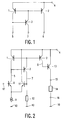
- reference numeral 1 denotes an input transistor of the bipolar pnp type
- 2 denotes an output transistor and 3 a bow transistor of the same conductivity type.
- the emitter connections of the input transistor 1 and the output transistor 2 are connected to a power supply 4, the base connections to the emitter connection of the bow transistor 3.
- the collector connection of the input transistor 1 is connected to an input connection 5, the collector connection of the output transistor 2 to an output connection 6 and the collector connection of the bow transistor 3 to a connection 7, via which a substantial proportion of the sum of the base currents of the input transistor 1 and the output transistor 2 is derived .
- a control transistor 8 is added to the current mirror arrangement described above, which has its collector connection connected to the input connection 5 and its emitter connection via an emitter current source 9 to ground 10 is.
- Another transistor 11 is connected with its collector connection to the power supply 4.
- the base connection of the further transistor 11 is connected to the connection 7, the emitter connection to the emitter connection of the control transistor 8.
- the connection 7 is also connected to ground 10 via a resistor 12.
- connection points 15 and 16 are shown symbolically.
- the control transistor 8, the further transistor 11 and the output stage transistor 13 in FIG. 2 are of the opposite conduction type like the input transistor 1, the output transistor 2 and the clip transistor 3, i.e. of the npn type.
- the output stage transistor 13 is connected as an emitter follower for the low-impedance supply of the consumer 14.
- the emitter current source 9 and the resistor 12 are preferably dimensioned in relation to the other components such that in normal operation, ie with the consumer 14 connected, the voltage caused by the current in the bow transistor 3 at the resistor 12 is less than a control voltage supplied via the base connection 17 of the control transistor 8.
- the further transistor 11 is then de-energized and does not influence the function of the current mirror arrangement, ie the input transistor 1 and the output transistor 2.
- the present invention solves the problem effectively with very little circuitry.
Landscapes
- Engineering & Computer Science (AREA)
- Microelectronics & Electronic Packaging (AREA)
- Physics & Mathematics (AREA)
- Nonlinear Science (AREA)
- Electromagnetism (AREA)
- General Physics & Mathematics (AREA)
- Radar, Positioning & Navigation (AREA)
- Automation & Control Theory (AREA)
- Amplifiers (AREA)
- Control Of Electrical Variables (AREA)
Abstract
- wenigstens einem einen ersten Leitungstyp aufweisenden Eingangstransistor, dessen Emitteranschluß mit einer Stromzuführung verbunden ist und dessen Kollektoranschluß einen Eingangsstrom führen kann,
- wenigstens einem den ersten Leitungstyp aufweisenden Ausgangstransistor, dessen Emitteranschluß mit der Stromzuführung und dessen Basisanschluß mit dem Basisanschluß des Eingangstransistors verbunden ist und dessen Kollektoranschluß ein Ausgangsstrom entnehmbar ist,
- sowie einem den ersten Leitungstyp aufweisen Bügeltransistor, dessen Emitteranschluß mit den Basisanschlüssen des Eingangstransistors und des Ausgangstransistors und dessen Basisanschluß mit dem Kollektoranschluß des Eingangstransistors verbunden und dessen Kollektoranschluß mit einem Bezugspotential gekoppelt ist.
- einen Steuertransistor von einem zweiten, dem ersten Leitungstyp entgegengesetzten Leitungstyp, wobei der Steuertransistor mit seinem Kollektoranschluß an den Kollektoranschluß des Eingangstransistors und mit seinem Emitteranschluß über eine Emitterstromquelle an das Bezugspotential angeschlossen und einem Basisanschluß des Steuertransistors eine Steuerspannung zum Steuern des Ausgangsstromes zuführbar ist,
- einen Widerstand, über den der Kollektoranschluß des Bügeltransistors mit dem Bezugspotential gekoppelt ist, sowie
- einen weiteren Transistor vom zweiten Leitungstyp, dessen Emitteranschluß mit dem Emitteranschluß des Steuertransistors, dessen Basisanschluß mit dem Kollektoranschluß des Bügeltransistors und dessen Kollektoranschluß mit der Stromzuführung verbunden ist.
Description
- Die Erfindung bezieht sich auf eine Stromspiegelanordnung mit
- wenigstens einem einen ersten Leitungstyp aufweisenden Eingangstransistor, dessen Emitteranschluß mit einer Stromzuführung verbunden ist und dessen Kollektoranschluß einen Eingangsstrom führen kann,
- wenigstens einem den ersten Leitungstyp aufweisenden Ausgangstransistor, dessen Emitteranschluß mit der Stromzuführung und dessen Basisanschluß mit dem Basisanschluß des Eingangstransistors verbunden ist und dessen Kollektoranschluß ein Ausgangsstrom entnehmbar ist,
- sowie einem den ersten Leitungstyp aufweisen Bügeltransistor, dessen Emitteranschluß mit den Basisanschlüssen des Eingangstransistors und des Ausgangstransistors und dessen Basisanschluß mit dem Kollektoranschluß des Eingangstransistors verbunden und dessen Kollektoranschluß mit einem Bezugspotential gekoppelt ist.
- Dabei dient der Bügeltransistor zum Aufnehmen der Basisströme des Eingangstransistors und des Ausgangstransistors derart, daß nur ein möglichst geringer Teil dieser Basisströme Einfluß auf das Verhältnis zwischen dem Eingangsstrom und dem Ausgangsstrom ausübt.
- Eine derartige Schaltungsanordnung ist aus der DE-PS 31 14 877 bekannt. In der dortigen Fig. 2 wird der Eingangsstrom von einer Stromquelle bewirkt, wohingegen der Ausgangsstrom über einen Verbraucher geführt wird.
- Im Normalbetrieb dieser Stromspiegelanordnung mit an den Ausgangstransistor angeschlossenem Verbraucher wird der Stromzuführung außer dem Eingangsstrom und dem Ausgangsstrom somit auch der vom Bügeltransistor geführte Strom entnommen, der um die Stromverstärkung eines der Transistoren vom ersten Leitungstyp geringer ist als die Summe aus Eingangsstrom und Ausgangsstrom. Da diese Stromverstärkung unter dem Einfluß verschiedener Fertigungs- und Betriebsparameter schwanken kann, stellt der Strom durch den Bügeltransistor und damit die Belastung der Stromzuführung eine stark streuende Größe dar.
- Wird der Verbraucher vom Ausgangstransistor abgetrennt und befindet sich die Stromspiegelanordnung somit im Leerlaufbetrieb, ergeben sich noch ungünstigere Verhältnisse. In diesem Betriebszustand ist das Stromspiegelverhältnis zwischen dem Eingangsstrom und dem Ausgangsstrom nicht mehr erfüllt. Während der Eingangstransistor jetzt nur noch sehr geringe Ströme führt, gerät der Ausgangstransistor in einen Sättigungszustand, in dem von der Stromzuführung über den Emitteranschluß und den Basisanschluß des Ausgangstransistors ein Strom in den Bügeltransistor fließt, der nahezu dem Gesamtstrom im Bügeltransistor entspricht. Wird jetzt von der Verbindung zwischen dem Kollektoranschluß des Eingangstransistors und dem Basisanschluß des Bügeltransistors ein vorgegebener Eingangsstrom entnommen, teilt sich dieser in einen Anteil über den Kollektoranschluß des Eingangstransistors und einen Anteil durch den Basisanschluß desBügeltransistors.
- Der Stromanteil durch den Basisanschluß des Bügeltransistors wird dabei so groß, daß der dadurch über den Emitteranschluß des Bügeltransistors und den Basisanschluß des Ausgangstransistors fließende Strom am Ausgangstransistor eine ebenso große Basis-Emitter-Spannung erzeugt, wie sie am Eingangstransistor vorliegt. Im Extremfall fließt dabei der vorgegebene Eingangsstrom fast ausschließlich durch den Basisanschluß des Bügeltransistors. Der Strom im Bügeltransistor ist dann im wesentlichen um die Stromverstärkung des Bügeltransistors höher als der Eingangsstrom. Dies stellt nicht nur eine wesentlich erhöhte Belastung der Stromzuführung gegenüber dem Normalbetrieb dar, sondern zusätzlich wird diese Belastung in der genannten Weise aufgrund der Streuungen der Stromverstärkung des Bügeltransistors stark streuen.
- Die Erfindung hat die Aufgabe, eine Stromspiegelanordnung der eingangs genannten Art in der Weise auszubilden, daß in allen Betriebszuständen eine definierte Belastung der Stromzuführung erreicht wird.
- Diese Aufgabe wird bei der gattungsgemäßen Stromspiegelanordnung erfindungsgemäß gelöst durch
- einen Steuertransistor von einem zweiten, dem ersten Leitungstyp entgegengesetzten Leitungstyp, wobei der Steuertransistor mit seinem Kollektoranschluß an den Kollektoranschluß des Eingangstransistors und mit seinem Emitteranschluß über eine Emitterstromquelle an das Bezugspotential angeschlossen und einem Basisanschluß des Steuertransistors eine Steuerspannung zum Steuern des Ausgangsstromes zuführbar ist,
- einen Widerstand, über den der Kollektoranschluß des Bügeltransistors mit dem Bezugspotential gekoppelt ist, sowie
- einen weiteren Transistor vom zweiten Leitungstyp, dessen Emitteranschluß mit dem Emitteranschluß des Steuertransistors, dessen Basisanschluß mit dem Kollektoranschluß des Bügeltransistors und dessen Kollektoranschluß mit der Stromzuführung verbunden ist.
- Bei der erfindungsgemäßen Stromspiegelanordnung wird der Strom durch den Bügeltransistor nicht unmittelbar, sondern über den Widerstand an das Bezugspotential geführt. Der weitere Transistor bildet mit dem Steuertransistor und der gemeinsamen Emitterstromquelle eine Differenzverstärkeranordnung, in der die Steuerspannung mit der durch den Strom im Bügeltransistor im Widerstand hervorgerufenen Spannung verglichen wird. Beim Anwachsen des Stromes durch den Bügeltransistor in der Weise, daß die Spannung am Widerstand die Steuerspannung übersteigt, wird der Strom der Emitterstromquelle aus dem Eingangstransistor in den weiteren Transistor umgeleitet und damit unmittelbar der Stromzuführung entnommen, nicht mehr jedoch dem Stromspiegel aus dem Eingangstransistor, dem Ausgangstransistor und dem Bügeltransistor. Dadurch wird der Strom über den Stromspiegel begrenzt. Der aus der Stromzuführung entnommene Strom ist nun wesentlich bestimmt durch den Quotienten aus der Steuerspannung und dem Widerstand sowie durch den Strom der Emitterstromquelle. Da diese Größen genau bestimmbar sind, erhält man in allen Betriebszuständen eine definierte Belastung der Stromzuführung. Dabei wird der Strom aus der Stromzuführung auch von der an dieser bereitgestellten Versorgungsspannung unabhängig.
- An dieser Stelle sei bemerkt, daß aus der japanischen Offenlegungsschrift 60-165112 (A) eine Stromspiegelanordnung mit einem Eingangstransistor, einem Ausgangstransistor und einem Bügeltransistor vom pnp-Typ bekannt ist, bei der der Kollektoranschluß des Bügeltransistors über einen Widerstand mit Masse verbunden ist. Mit dem Emitteranschluß des Bügeltransistors und den Basisanschlüssen des Eingangstransistors und des Ausgangstransistors bzw. der Ausgangstransistoren ist der Kollektoranschluß eines Transistors verbunden, dessen Basisanschluß mit dem Kollektoranschluß des Bügeltransistors und dessen Emitteranschluß mit Masse verbunden ist. In dieser bekannten Schaltungsanordnung übernimmt der Transistor vom Bügeltransistor einen Teil des Emitterstromes, um den Basisstrom des Bügeltransistors zu verringern. Dadurch soll offenbar das Spiegelverhältnis der bekannten Stromspiegelanordnung auch bei mehreren Ausgangstransistoren und damit einem höheren Strom im Bügeltransistor präziser ausgebildet werden. Da jedoch sowohl der Bügeltransistor als auch der zusätzlich eingeführte Transistor ihre Ströme aus den Basisanschlüssen des Eingangstransistors und der Ausgangstransistoren entnehmen, werden die eingangs erläuterten Streuungen der Ströme aus der Stromzuführung nicht behoben.
- In einer vorteilhaften Ausgestaltung enthält die erfindungsgemäße Stromspiegelanordnung einen den zweiten Leitungstyp aufweisenden Endstufentransistor, dessen Kollektoranschluß mit der Stromzuführung und dessen Basisanschluß mit dem Kollektoranschluß des Ausgangstransistors verbunden und dessen Emitteranschluß mit einer Last koppelbar ist. Durch diesen Entstufentransistor wird der Ausgangs transistor vom Strom durch den Verbraucher entlastet.
- Vorzugsweise wird bei der erfindungsgemäßen Stromspiegelanordnung als erster Leitungstyp der pnp-Typ und als zweiter Leitungstyp der npn-Typ bipolarer Transistoren bezeichnet. Eingangs-, Ausgangs- und Bügeltransistor sind dann vom pnp-Typ. Bipolare pnp-Transistoren weisen vielfach eine geringere Stromverstärkung als npn-Transistoren auf, so daß ihre Basisströme im Verhältnis größer sind und daher zu größeren Abweichungen in Stromspiegeln, aber auch zu größeren Belastungen insbesondere des Bügeltransistors führen. Daher ist eine Anwendung der Erfindung auf diesen Leitungstyp besonders vorteilhaft; jedoch ist auch eine umgekehrte Zuordnung des Leitungstyps möglich.
- Ein Ausführungsbeispiel ist in der Zeichnungd dargestellt und wird im nachfolgenden näher erläutert. Dabei zeigt
- Fig. 1 eine Stromspiegelanordnung nach dem Stand der Technik,
- Fig. 2 eine erfindungsgemäße Stromspiegelanordnung.
- In Fig. 1 ist mit dem Bezugszeichen 1 ein Eingangstransistor vom bipolaren pnp-Typ bezeichnet, wohingegen mit 2 ein Ausgangstransistor und mit 3 ein Bügeltransistor des gleichen Leitungstyps benannt ist. Die Emitteranschlüsse des Eingangstransistors 1 und des Ausgangstransistors 2 sind mit einer Stromzuführung 4, die Basisanschlüsse mit dem Emitteranschluß des Bügeltransistors 3 verbunden. Der Kollektoranschluß des Eingangstransistors 1 ist mit einem Eingangsanschluß 5, der Kollektoranschluß des Ausgangstransistors 2 mit einem Ausgangsanschluß 6 und der Kollektoranschluß des Bügeltransistors 3 mit einem Anschluß 7 verbunden, über den ein wesentlicher Anteil der Summe der Basisströme des Eingangstransistors 1 und des Ausgangstransistors 2 abgeleitet wird.
- In Fig. 2, in der mit Fig. 1 übereinstimmende Elemente wieder mit denselben Bezugszeichen versehen sind, ist der vorstehend beschriebenen Stromspiegelanordnung ein Steuertransistor 8 hinzugefügt, der mit seinem Kollektoranschluß mit dem Eingangsanschluß 5 und mit seinem Emitteranschluß über eine Emitterstromquelle 9 mit Masse 10 verbunden ist. Ein weiterer Transistor 11 ist mit seinem Kollektoranschluß an die Stromzuführung 4 angeschlossen. Der Basisanschluß des weiteren Transistors 11 ist an den Anschluß 7, der Emitteranschluß an den Emitteranschluß des Steuertransistors 8 geführt. Der Anschluß 7 ist außerdem über einen Widerstand 12 mit Masse 10 verbunden.
- Weiterhin ist an den Kollektoranschluß des Ausgangstransistors 2, d.h. an den Ausgangsanschluß 6, der Basisanschluß eines Endstufentransistors 13 angeschlossen, dessen Kollektoranschluß an die Stromzuführung 4 angeschlossen ist und dessen Emitteranschluß über einen Verbraucher 14 an Masse 10 geführt ist. Zum Anschluß des Verbrauchers 14 sind symbolisch Anschlußpunkte 15 und 16 eingezeichnet.
- Der Steuertransistor 8, der weitere Transistor 11 und der Endstufentransistor 13 sind in Fig. 2 vom entgegengesetzten Leitungstyp wie der Eingangstransistor 1, der Ausgangstransistor 2 und der Bügeltransistor 3, d.h. vom npn-Typ. Der Endstufentransistor 13 ist als Emitterfolger zur niederohmigen Speisung des Verbrauchers 14 geschaltet.
- In der Stromspiegelanordnung nach Fig. 2 sind die Emitterstromquelle 9 und der Widerstand 12 im Verhältnis zu den übrigen Bauteilen bevorzugt derart dimensioniert, daß im Normalbetrieb, d.h. mit angeschlossenem Verbraucher 14, die durch den Strom im Bügeltransistor 3 am Widerstand 12 hervorgerufene Spannung geringer ist als eine über den Basisanschluß 17 des Steuertransistors 8 zugeführte Steuerspannung. Der weitere Transistor 11 ist dann stromlos und beeinflußt die Funktion der Stromspiegelanordnung, d.h. des Eingangstransistors 1 und des Ausgangstransistors 2 nicht.
- Steigt im Leerlaufbetrieb, d.h. nach Abtrennen des Verbrauchers 14 an den Anschlußpunkten 15, 16, der Strom im Bügeltransistor 3 an, übersteigt die Spannung am Widerstand 12 die Steuerspannung am Basisanschluß 17. Der Strom der Emitterstromquelle 9 fließt nun von der Stromzuführung 4 unmittelbar über den weiteren Transistor 11. Dadurch wird ein weiteres Anwachsen des Stromes im Bügeltransistor 3 und damit eine Vergrößerung der Stromentnahme aus der Stromzuführung 4 unterbunden; vielmehr wird aus der Stromzuführung 4 zu liefernde Strom auf einen definierten Wert begrenzt, der durch den Strom der Emitterstromquelle 9 und das Verhältnis der Steuerspannung und des Widerstands 12 bestimmt wird.
- Die vorliegende Erfindung löst die hergestellte Aufgabe wirkungsvoll mit sehr geringem Schaltungsaufwand.
Claims (3)
- Stromspiegelanordnung mit- wenigstens einem einen ersten Leitungstyp aufweisenden Eingangstransistor, dessen Emitteranschluß mit einer Stromzuführung verbunden ist und dessen Kollektoranschluß einen Eingangsstrom führen kann,- wenigstens einem den ersten Leitungstyp aufweisenden Ausgangstransistor, dessen Emitteranschluß mit der Stromzuführung und dessen Basisanschluß mit dem Basisanschluß des Eingangstransistors verbunden ist und dessen Kollektoranschluß ein Ausgangsstrom entnehmbar ist,- sowie einem den ersten Leitungstyp aufweisen Bügeltransistor, dessen Emitteranschluß mit den Basisanschlüssen des Eingangstransistors und des Ausgangstransistors und dessen Basisanschluß mit dem Kollektoranschluß des Eingangstransistors verbunden und dessen Kollektoranschluß mit einem Bezugspotential gekoppelt ist,gekennzeichnet durch- einen Steuertransistor von einem zweiten, dem ersten Leitungstyp entgegengesetzten Leitungstyp, wobei der Steuertransistor mit seinem Kollektoranschluß an den Kollektoranschluß des Eingangstransistors und mit seinem Emitteranschluß über eine Emitterstromquelle an das Bezugspotential angeschlossen und einem Basisanschluß des Steuertransistors eine Steuerspannung zum Steuern des Ausgangsstromes zuführbar ist,- einen Widerstand, über den der Kollektoranschluß des Bügeltransistors mit dem Bezugspotential gekoppelt ist, sowie- einen weiteren Transistor vom zweiten Leitungstyp, dessen Emitteranschluß mit dem Emitteranschluß des Steuertransistors, dessen Basisanschluß mit dem Kollektoranschluß des Bügeltransistors und dessen Kollektoranschluß mit der Stromzuführung verbunden ist.
- Stromspiegelanordnung nach Anspruch 1, gekennzeichnet durch einen den zweiten Leitungstyp aufweisenden Endstufentransistor, dessen Kollektoranschluß mit der Stromzuführung und dessen Basisanschluß mit dem Kollektoranschluß des Ausgangstransistors verbunden und dessen Emitteranschluß mit einer Last koppelbar ist.
- Stromspiegelanordnung nach Anspruch 1 oder 2, dadurch gekennzeichnet, daß der erste Leitungstyp den pnp-Typ und der zweite Leitungstyp den npn-Typ bezeichnet.
Applications Claiming Priority (2)
| Application Number | Priority Date | Filing Date | Title |
|---|---|---|---|
| DE19529059A DE19529059A1 (de) | 1995-08-08 | 1995-08-08 | Stromspiegelanordnung |
| DE19529059 | 1995-08-08 |
Publications (3)
| Publication Number | Publication Date |
|---|---|
| EP0758108A2 true EP0758108A2 (de) | 1997-02-12 |
| EP0758108A3 EP0758108A3 (de) | 1997-03-19 |
| EP0758108B1 EP0758108B1 (de) | 1999-12-01 |
Family
ID=7768936
Family Applications (1)
| Application Number | Title | Priority Date | Filing Date |
|---|---|---|---|
| EP96202214A Expired - Lifetime EP0758108B1 (de) | 1995-08-08 | 1996-08-07 | Stromspiegelanordnung |
Country Status (4)
| Country | Link |
|---|---|
| US (1) | US5682094A (de) |
| EP (1) | EP0758108B1 (de) |
| JP (1) | JPH09139636A (de) |
| DE (2) | DE19529059A1 (de) |
Cited By (1)
| Publication number | Priority date | Publication date | Assignee | Title |
|---|---|---|---|---|
| CN113168199A (zh) * | 2018-11-26 | 2021-07-23 | 株式会社村田制作所 | 电流输出电路 |
Families Citing this family (1)
| Publication number | Priority date | Publication date | Assignee | Title |
|---|---|---|---|---|
| DE19930381A1 (de) * | 1999-07-01 | 2001-01-04 | Philips Corp Intellectual Pty | Stromspiegelanordnung |
Family Cites Families (15)
| Publication number | Priority date | Publication date | Assignee | Title |
|---|---|---|---|---|
| NL169239C (nl) * | 1971-10-21 | 1982-06-16 | Philips Nv | Stroomversterker. |
| US3952257A (en) * | 1974-10-29 | 1976-04-20 | Rca Corporation | Current proportioning circuits |
| US4045694A (en) * | 1975-09-26 | 1977-08-30 | Rca Corporation | Current divider |
| US4260945A (en) * | 1979-04-06 | 1981-04-07 | Rca Corporation | Regulated current source circuits |
| JPS605085B2 (ja) * | 1980-04-14 | 1985-02-08 | 株式会社東芝 | カレントミラ−回路 |
| US4525683A (en) * | 1983-12-05 | 1985-06-25 | Motorola, Inc. | Current mirror having base current error cancellation circuit |
| US4525682A (en) * | 1984-02-07 | 1985-06-25 | Zenith Electronics Corporation | Biased current mirror having minimum switching delay |
| JPS60165112A (ja) * | 1984-02-08 | 1985-08-28 | Toshiba Corp | カレントミラ−回路 |
| GB2163614A (en) * | 1984-08-22 | 1986-02-26 | Philips Electronic Associated | Battery economising circuit |
| US4814724A (en) * | 1986-07-15 | 1989-03-21 | Toko Kabushiki Kaisha | Gain control circuit of current mirror circuit type |
| US4771228A (en) * | 1987-06-05 | 1988-09-13 | Vtc Incorporated | Output stage current limit circuit |
| DE68910428T2 (de) * | 1988-08-19 | 1994-05-11 | Philips Nv | Spannungs-/Stromwandler. |
| US4961046A (en) * | 1988-08-19 | 1990-10-02 | U.S. Philips Corp. | Voltage-to-current converter |
| JPH0535350A (ja) * | 1991-07-26 | 1993-02-12 | Nec Yamagata Ltd | 定電流源 |
| US5311146A (en) * | 1993-01-26 | 1994-05-10 | Vtc Inc. | Current mirror for low supply voltage operation |
-
1995
- 1995-08-08 DE DE19529059A patent/DE19529059A1/de not_active Withdrawn
-
1996
- 1996-08-05 US US08/692,146 patent/US5682094A/en not_active Expired - Fee Related
- 1996-08-05 JP JP8205976A patent/JPH09139636A/ja active Pending
- 1996-08-07 DE DE59603762T patent/DE59603762D1/de not_active Expired - Fee Related
- 1996-08-07 EP EP96202214A patent/EP0758108B1/de not_active Expired - Lifetime
Cited By (1)
| Publication number | Priority date | Publication date | Assignee | Title |
|---|---|---|---|---|
| CN113168199A (zh) * | 2018-11-26 | 2021-07-23 | 株式会社村田制作所 | 电流输出电路 |
Also Published As
| Publication number | Publication date |
|---|---|
| EP0758108A3 (de) | 1997-03-19 |
| DE19529059A1 (de) | 1997-02-13 |
| DE59603762D1 (de) | 2000-01-05 |
| EP0758108B1 (de) | 1999-12-01 |
| JPH09139636A (ja) | 1997-05-27 |
| US5682094A (en) | 1997-10-28 |
Similar Documents
| Publication | Publication Date | Title |
|---|---|---|
| DE3713376A1 (de) | Komparator mit erweitertem eingangsgleichtaktspannungsbereich | |
| DE69113523T2 (de) | Emittergeerdete Verstärkerschaltung mit Vorspannungsschaltung. | |
| DE2653624A1 (de) | Videosignalverstaerker | |
| DE2461163C3 (de) | Monolithischer Leistungsverstärker | |
| DE3416850C2 (de) | ||
| DE3230429C2 (de) | ||
| DE3545392C2 (de) | ||
| DE2122768A1 (de) | Spannungsregler fur negative Spannungen | |
| DE2924171C2 (de) | ||
| DE4111495A1 (de) | Gegentakt-endstufe | |
| EP0374288A1 (de) | Integrierbare Schaltungsanordnung zur Rückstromverringerung bei einem invers betriebenen Transistor | |
| EP0758108B1 (de) | Stromspiegelanordnung | |
| DE2349462A1 (de) | Stabilisationsschaltung fuer einen konstanten strom | |
| DE3115051C2 (de) | Spannungs/Strom-Wandlerschaltung | |
| DE3824105A1 (de) | Spannungsregelschaltung | |
| EP0904576B1 (de) | Stromversorgungsschaltung | |
| DE3603799A1 (de) | Stromspiegelschaltung | |
| DE4136605A1 (de) | Verstaerker | |
| EP0107133B1 (de) | Schaltungsanordnung zum Speisen einer eine konstante Betriebsspannung liefernden Stromversorgungseinrichtung | |
| DE3836836A1 (de) | Umsetzschaltung | |
| DE2621083C2 (de) | Differenzverstärker | |
| DE68918750T2 (de) | Niederspannungsgesteuerte elektronische Schaltung in Bereitschaftsstellung mit verzögertem Abschalten. | |
| DE3032970C2 (de) | Schaltungsanordnung zur Symmetrierung der Arbeitspunkte bei elektronisch gleichstromgespeisten Anschlußleitungen in Fernmelde-, insbesondere Fernsprechvermittlungsanlagen | |
| DE3783672T2 (de) | Schaltung mit gemeinsamer verbindung und ausschaltfunktion. | |
| DE2009039A1 (de) | Schaltung mit Überstromschutz |
Legal Events
| Date | Code | Title | Description |
|---|---|---|---|
| PUAI | Public reference made under article 153(3) epc to a published international application that has entered the european phase |
Free format text: ORIGINAL CODE: 0009012 |
|
| PUAL | Search report despatched |
Free format text: ORIGINAL CODE: 0009013 |
|
| AK | Designated contracting states |
Kind code of ref document: A2 Designated state(s): DE FR GB IT |
|
| AK | Designated contracting states |
Kind code of ref document: A3 Designated state(s): DE FR GB IT |
|
| 17P | Request for examination filed |
Effective date: 19970919 |
|
| GRAG | Despatch of communication of intention to grant |
Free format text: ORIGINAL CODE: EPIDOS AGRA |
|
| 17Q | First examination report despatched |
Effective date: 19990127 |
|
| GRAG | Despatch of communication of intention to grant |
Free format text: ORIGINAL CODE: EPIDOS AGRA |
|
| GRAH | Despatch of communication of intention to grant a patent |
Free format text: ORIGINAL CODE: EPIDOS IGRA |
|
| GRAH | Despatch of communication of intention to grant a patent |
Free format text: ORIGINAL CODE: EPIDOS IGRA |
|
| GRAA | (expected) grant |
Free format text: ORIGINAL CODE: 0009210 |
|
| AK | Designated contracting states |
Kind code of ref document: B1 Designated state(s): DE FR GB IT |
|
| PG25 | Lapsed in a contracting state [announced via postgrant information from national office to epo] |
Ref country code: IT Free format text: LAPSE BECAUSE OF FAILURE TO SUBMIT A TRANSLATION OF THE DESCRIPTION OR TO PAY THE FEE WITHIN THE PRESCRIBED TIME-LIMIT;WARNING: LAPSES OF ITALIAN PATENTS WITH EFFECTIVE DATE BEFORE 2007 MAY HAVE OCCURRED AT ANY TIME BEFORE 2007. THE CORRECT EFFECTIVE DATE MAY BE DIFFERENT FROM THE ONE RECORDED. Effective date: 19991201 |
|
| REF | Corresponds to: |
Ref document number: 59603762 Country of ref document: DE Date of ref document: 20000105 |
|
| RAP4 | Party data changed (patent owner data changed or rights of a patent transferred) |
Owner name: KONINKLIJKE PHILIPS ELECTRONICS N.V. Owner name: PHILIPS CORPORATE INTELLECTUAL PROPERTY GMBH |
|
| GBT | Gb: translation of ep patent filed (gb section 77(6)(a)/1977) |
Effective date: 20000121 |
|
| ET | Fr: translation filed | ||
| PLBE | No opposition filed within time limit |
Free format text: ORIGINAL CODE: 0009261 |
|
| STAA | Information on the status of an ep patent application or granted ep patent |
Free format text: STATUS: NO OPPOSITION FILED WITHIN TIME LIMIT |
|
| 26N | No opposition filed | ||
| PGFP | Annual fee paid to national office [announced via postgrant information from national office to epo] |
Ref country code: FR Payment date: 20010824 Year of fee payment: 6 |
|
| PGFP | Annual fee paid to national office [announced via postgrant information from national office to epo] |
Ref country code: GB Payment date: 20010831 Year of fee payment: 6 |
|
| PGFP | Annual fee paid to national office [announced via postgrant information from national office to epo] |
Ref country code: DE Payment date: 20011015 Year of fee payment: 6 |
|
| REG | Reference to a national code |
Ref country code: GB Ref legal event code: IF02 |
|
| PG25 | Lapsed in a contracting state [announced via postgrant information from national office to epo] |
Ref country code: GB Free format text: LAPSE BECAUSE OF NON-PAYMENT OF DUE FEES Effective date: 20020807 |
|
| PG25 | Lapsed in a contracting state [announced via postgrant information from national office to epo] |
Ref country code: DE Free format text: LAPSE BECAUSE OF NON-PAYMENT OF DUE FEES Effective date: 20030301 |
|
| GBPC | Gb: european patent ceased through non-payment of renewal fee |
Effective date: 20020807 |
|
| PG25 | Lapsed in a contracting state [announced via postgrant information from national office to epo] |
Ref country code: FR Free format text: LAPSE BECAUSE OF NON-PAYMENT OF DUE FEES Effective date: 20030430 |
|
| REG | Reference to a national code |
Ref country code: FR Ref legal event code: ST |