EP0759622A2 - Nichtflüchtiger Speicher und Verfahren zu seiner Programmierung - Google Patents
Nichtflüchtiger Speicher und Verfahren zu seiner Programmierung Download PDFInfo
- Publication number
- EP0759622A2 EP0759622A2 EP96113258A EP96113258A EP0759622A2 EP 0759622 A2 EP0759622 A2 EP 0759622A2 EP 96113258 A EP96113258 A EP 96113258A EP 96113258 A EP96113258 A EP 96113258A EP 0759622 A2 EP0759622 A2 EP 0759622A2
- Authority
- EP
- European Patent Office
- Prior art keywords
- voltage
- programming
- drain
- memory device
- gate
- Prior art date
- Legal status (The legal status is an assumption and is not a legal conclusion. Google has not performed a legal analysis and makes no representation as to the accuracy of the status listed.)
- Granted
Links
Images







Classifications
-
- G—PHYSICS
- G11—INFORMATION STORAGE
- G11C—STATIC STORES
- G11C16/00—Erasable programmable read-only memories
- G11C16/02—Erasable programmable read-only memories electrically programmable
- G11C16/06—Auxiliary circuits, e.g. for writing into memory
- G11C16/34—Determination of programming status, e.g. threshold voltage, overprogramming or underprogramming, retention
- G11C16/3436—Arrangements for verifying correct programming or erasure
- G11C16/3468—Prevention of overerasure or overprogramming, e.g. by verifying whilst erasing or writing
- G11C16/3486—Circuits or methods to prevent overprogramming of nonvolatile memory cells, e.g. by detecting onset or cessation of current flow in cells and using the detector output to terminate programming
-
- G—PHYSICS
- G11—INFORMATION STORAGE
- G11C—STATIC STORES
- G11C11/00—Digital stores characterised by the use of particular electric or magnetic storage elements; Storage elements therefor
- G11C11/56—Digital stores characterised by the use of particular electric or magnetic storage elements; Storage elements therefor using storage elements with more than two stable states represented by steps, e.g. of voltage, current, phase, frequency
- G11C11/5621—Digital stores characterised by the use of particular electric or magnetic storage elements; Storage elements therefor using storage elements with more than two stable states represented by steps, e.g. of voltage, current, phase, frequency using charge storage in a floating gate
-
- G—PHYSICS
- G11—INFORMATION STORAGE
- G11C—STATIC STORES
- G11C11/00—Digital stores characterised by the use of particular electric or magnetic storage elements; Storage elements therefor
- G11C11/56—Digital stores characterised by the use of particular electric or magnetic storage elements; Storage elements therefor using storage elements with more than two stable states represented by steps, e.g. of voltage, current, phase, frequency
- G11C11/5621—Digital stores characterised by the use of particular electric or magnetic storage elements; Storage elements therefor using storage elements with more than two stable states represented by steps, e.g. of voltage, current, phase, frequency using charge storage in a floating gate
- G11C11/5628—Programming or writing circuits; Data input circuits
-
- G—PHYSICS
- G11—INFORMATION STORAGE
- G11C—STATIC STORES
- G11C16/00—Erasable programmable read-only memories
- G11C16/02—Erasable programmable read-only memories electrically programmable
- G11C16/04—Erasable programmable read-only memories electrically programmable using variable threshold transistors, e.g. FAMOS
- G11C16/0408—Erasable programmable read-only memories electrically programmable using variable threshold transistors, e.g. FAMOS comprising cells containing floating gate transistors
- G11C16/0416—Erasable programmable read-only memories electrically programmable using variable threshold transistors, e.g. FAMOS comprising cells containing floating gate transistors comprising cells containing a single floating gate transistor and no select transistor, e.g. UV EPROM
-
- G—PHYSICS
- G11—INFORMATION STORAGE
- G11C—STATIC STORES
- G11C16/00—Erasable programmable read-only memories
- G11C16/02—Erasable programmable read-only memories electrically programmable
- G11C16/04—Erasable programmable read-only memories electrically programmable using variable threshold transistors, e.g. FAMOS
- G11C16/0408—Erasable programmable read-only memories electrically programmable using variable threshold transistors, e.g. FAMOS comprising cells containing floating gate transistors
- G11C16/0441—Erasable programmable read-only memories electrically programmable using variable threshold transistors, e.g. FAMOS comprising cells containing floating gate transistors comprising cells containing multiple floating gate devices, e.g. separate read-and-write FAMOS transistors with connected floating gates
-
- G—PHYSICS
- G11—INFORMATION STORAGE
- G11C—STATIC STORES
- G11C16/00—Erasable programmable read-only memories
- G11C16/02—Erasable programmable read-only memories electrically programmable
- G11C16/06—Auxiliary circuits, e.g. for writing into memory
- G11C16/34—Determination of programming status, e.g. threshold voltage, overprogramming or underprogramming, retention
- G11C16/3436—Arrangements for verifying correct programming or erasure
- G11C16/3468—Prevention of overerasure or overprogramming, e.g. by verifying whilst erasing or writing
-
- G—PHYSICS
- G11—INFORMATION STORAGE
- G11C—STATIC STORES
- G11C16/00—Erasable programmable read-only memories
- G11C16/02—Erasable programmable read-only memories electrically programmable
- G11C16/06—Auxiliary circuits, e.g. for writing into memory
- G11C16/34—Determination of programming status, e.g. threshold voltage, overprogramming or underprogramming, retention
- G11C16/3436—Arrangements for verifying correct programming or erasure
- G11C16/3468—Prevention of overerasure or overprogramming, e.g. by verifying whilst erasing or writing
- G11C16/3481—Circuits or methods to verify correct programming of nonvolatile memory cells whilst programming is in progress, e.g. by detecting onset or cessation of current flow in cells and using the detector output to terminate programming
-
- G—PHYSICS
- G11—INFORMATION STORAGE
- G11C—STATIC STORES
- G11C2211/00—Indexing scheme relating to digital stores characterized by the use of particular electric or magnetic storage elements; Storage elements therefor
- G11C2211/56—Indexing scheme relating to G11C11/56 and sub-groups for features not covered by these groups
- G11C2211/561—Multilevel memory cell aspects
- G11C2211/5613—Multilevel memory cell with additional gates, not being floating or control gates
-
- G—PHYSICS
- G11—INFORMATION STORAGE
- G11C—STATIC STORES
- G11C2211/00—Indexing scheme relating to digital stores characterized by the use of particular electric or magnetic storage elements; Storage elements therefor
- G11C2211/56—Indexing scheme relating to G11C11/56 and sub-groups for features not covered by these groups
- G11C2211/562—Multilevel memory programming aspects
- G11C2211/5624—Concurrent multilevel programming and programming verification
Definitions
- the present invention relates to a nonvolatile memory and a method of programming the nonvolatile memory.
- the packing density of a conventional nonvolatile memory corresponds in a one to one fashion to the number of memory cells.
- a multibit cell stores data of over two bits in one memory cell, thus enhancing the density of data on the same chip area without reducing the size of the memory cell.
- threshold voltage levels For the multibit cell, more than three threshold voltage levels should be programmed on respective memory cells. For instance, in order to store data of two bits for every cell, the respective cells must be programmed in 2 2 , that is, four, threshold levels.
- the four threshold levels correspond to logic states 00, 01, 10, and 11, respectively.
- the most critical problem is that the respective threshold voltage levels have a statistical distribution.
- the distribution value is about 0.5V.
- a series of voltage pulses are applied to the cells in order to program the nonvolatile memory cell at intended threshold levels.
- a read operation is performed between the respective programming voltage pulses.
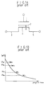
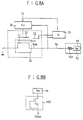
- Fig. 1A illustrates the symbol and circuit diagram of the nonvolatile memory proposed by Cernea.
- the nonvolatile memory cell is composed of a control gate 1, floating gate 2, source 3, channel area 4, and drain 5.
- Cernea's method a program gate for programming is not used separately. Further, this method does not use a structure in which a programming current path and sensing (or verifying) current path are completely separated. For this reason, in Cernea's method, programming and sensing are difficult to optimize individually. The programming current and monitoring current are not separated so that the cell's threshold voltages are difficult to control and adjust directly. Conventionally, however, multi-level programming has been performed in such a manner that the voltages applied to the respective parts of a memory cell are fixed, and reference currents corresponding to the respective levels are varied. In this method, as shown in Fig. 1B, reference currents for detection have no explicit relation with the cell threshold voltages, and are not linear with them.
- the cell structure of an EEPROM or a flash EEPROM is roughly divided into two parts, depending upon where the floating gate is placed on the channel area.
- the first structure is a simple-stacked gate structure in which the floating gate completely covers the cell channel area.
- the second one is a split-channel structure in which the floating gate covers only part of the channel area between the source and drain.
- a portion where the floating gate is not present is called a transfer transistor, which is introduced to eliminate over-erasure problem.
- the split-channel cell is undesirably larger than the simple-stacked gate structure.
- flash EEPROM depends on whether a double polysilicon gate or triple polysilicon gate is used.
- the double polysilicon gate is usually employed in the simple-stacked structure.
- the triple polysilicon gate is used in the split-channel cell.
- the EEPROM or flash EEPROM memory cells are disclosed in detail in United States Patent No. 5,268,318.
- the third gate in the triple polysilicon gate is an erasing gate used merely for data erasure. In the flash EEPROM, erasure is performed in units of blocks made up of a plurality of cells.
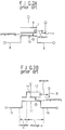
- Fig. 2A is a diagram of a conventional nonvolatile memory cell having a simple-stacked gate.
- Fig. 2B is a diagram of a conventional nonvolatile memory cell having a split-channel structure.
- Figs. 2A and 2B show programming and erasing processes as well as the structure of the conventional nonvolatile memory cells.
- the conventional stacked gate memory cell includes a control gate 6, a floating gate 7, a source 8, a drain 9, a channel area 10, and an erasing gate 11.
- the conventional split channel memory cell includes a control gate 13, a floating gate 14, a source 15, a drain 16, a channel area 17, and an erasing gate 18.
- erasing gates 11 and 18 are not required for programming. Therefore, during programming, the conventional cells of Figs. 2A and 2B have substantially the same structure as the double polysilicon gate.
- programming is carried out only with the control gate, source and/or drain electrodes so that it is difficult to separate the program current path and verification (sensing) current path within the memory cell for programming and verification. Accordingly, it is difficult to control the multi-levels directly and effectively.
- the present invention has been made in view of the above circumstances and has as an object to provide a nonvolatile memory and a method of programming the nonvolatile memory, in which verification and programming can be carried out more directly and effectively.
- the memory cell of a nonvolatile memory device of this invention comprises: a floating gate; a programming region having a first current path to the floating gate, for programming by providing charge carriers to the floating gate through the first current path or extracting charge carriers stored in the floating gate; and a verification region having a second current path separated from the first current path, for verifying the charge amount of the floating gate through the second current path.
- the method of the invention is characterized by: providing charge carriers to said floating gate through a first current path or extracting charge carriers stored in said floating gate; and verifying the charge amount of said floating gate through a second current path separated from said first current path.
- a nonvolatile memory device the memory cell of which comprising: a floating gate; a program gate for providing charge carriers to the floating gate for the purpose of programming; a control gate for controlling the amount of charge carriers provided to the floating gate for programming; and a field effect transistor, including the floating gate, a source, a drain, and a channel area between the source and drain, and for verifying charge carriers provided to the floating gate.
- a method of programming the nonvolatile memory cell comprising the steps of: supplying a first voltage to the control gate and a second voltage to the program gate so that charge carriers for programming are fed to the floating gate from the program gate and an inversion layer is formed in the channel area; and monitoring the conductivity of the inversion layer and stopping the supply of at least one of the first voltage and second voltage to the control gate and the program gate when the monitored conductivity reaches a reference value.
- a nonvolatile memory device comprising: a floating gate divided into first and second areas; a programming field effect transistor including the first area corresponding to part of the floating gate, a first drain, and a common source, a channel area between the first drain and the common source and having a first threshold voltage for supplying charge carriers to the floating gate for the purpose of programming; a control gate for controlling the amount of charge carriers supplied to the floating gate for programming; and a monitoring field effect transistor including the second area of the floating gate excluding the first area, a second drain, and the common source, a channel area between the second drain and the common source and having a second threshold voltage for verifying the amount of charge carriers supplied to the floating gate.
- a nonvolatile memory cell comprising a control gate, a floating gate divided into first and second areas; a programming field effect transistor including the first area of the floating gate, a first drain, a common source, and a first channel area between the first drain and common source, and having a first threshold voltage; and a monitoring field effect transistor including the second area of the floating gate, a second drain, and the common source, and a second channel area between the second drain and common source, and having a second threshold voltage
- a method of programming the nonvolatile memory cell comprising the steps of: supplying a first voltage to the control gate and a second voltage to the first drain so that charge carriers for programming are fed to the floating gate through the first channel area for programming and an inversion layer is formed in the second channel area; and monitoring the conductivity of the inversion layer and stopping the supply of at least one of the first voltage and second voltage to the control gate and the first drain when the monitored conductivity reaches a reference value.
- the programming process and the verification process can be carried out simultaneously, if desired.
- a nonvolatile memory cell comprises a floating gate, a programming region, having a first current path to the floating gate, for programming by providing charge carriers to the floating gate through the first current path or extracting charge carriers stored in the floating gate, and a verification region, having a second current path separated from the first current path for verifying the charge amount of the floating gate through the second current path during programming.
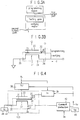
- a nonvolatile memory cell comprises a floating gate 31, a program gate 32 for providing negative charges (electrons) or positive charges (holes) to floating gate 31 for the purpose of double or multi-level programming, a control gate 33 for providing voltage to floating gate 31 by capacitive coupling between the control gate and floating gate and controlling the amount of charges provided to floating gate 31 from program gate 32 for the purpose of programming, and a transistor 34 for verifying (or sensing) charges provided to floating gate 31 during double or multi-level programming.
- transistor 34 includes floating gate 31, a source 35, a drain 36, and a channel area 37 between source 35 and drain 36.
- the nonvolatile memory of the present invention is constructed to perform double or multi-level programming, using a third program gate 32, and to verify whether the programming is completed or not by checking the amount of charges supplied to floating gate 31 during the double or multi-level programming.
- Control gate 33, floating gate 31, and program gate 32 may perform only double or multi-level programming. Conversely, transistor 34 may merely perform monitoring of the amount of charges of floating gate 31 in order to verify whether programming is completed or proceeding.
- the programming region is separated completely from the verifying region. These two regions are connected through floating gate 31.
- Floating gate 31 and program gate 32 corresponding to the programming region can be regarded as forming a tunnel diode. Programming is performed by a tunnelling mechanism through the tunnel diode.
- the prior art does not use program gate 32, and performs both programming and verification through drain 36 and channel area 37 of transistor 34.
- the present invention is distinctive from the prior art.
- the programming method of the present invention includes voltage detection and current detection.
- Fig. 4 includes a first voltage source 38, second voltage source 39, third voltage source 40, fourth voltage source 41, current detector 42, and nonvolatile memory 100 such as that shown in Fig. 3.
- Reference character P S indicates an externally supplied programming start signal.
- Reference character V ST indicates a programming stop signal.
- Voltage V C,i has values that vary with the respective programming levels.
- Second voltage source 39 applies a voltage V P to program gate 32 for the double or multi-level programming.
- Voltage V P always has a fixed negative value.
- Third voltage source 40 induces a voltage V D to drain 36 in order to monitor the state of programming, that is, drain current I D,i (t), during the double or multi-level programming.
- Fourth voltage source 41 supplies a voltage V S to source 35.
- voltage V S may be ground.
- I D,i (t) indicates the current flowing through drain 36 at time (t).
- Current detector 42 has a threshold current value Ith, and produces a programming stop signal V ST when current I D,i (t) flowing through drain 36 reaches the threshold current Ith during an ith threshold level programming.
- Time t p,i refers to the time when the ith threshold programming is completed.
- threshold current Ith of current detector 42 can be defined by a value near the threshold region of the transistor, which can be greater than or equal to zero.
- reference current I REF greater than the threshold current can also be used for describing the present invention, resulting in the same conclusion.
- reference current I REF is large, the initial voltage at floating gate 31 V F, i (0) should be large as well, so as to satisfy I D,i (0)>I REF at the initial stage of the multi-level programming.
- voltage V c,i in order to increase the initial voltage V F,i (0), voltage V c,i must also be increased.
- Current I D,i (t) indicates the current value of drain 36 triggered by voltage V F,i (t) at floating gate 31 during the ith level programming.
- the current value has the largest value at the initial stage of programming, and is reduced as programming proceeds.
- threshold current Ith of current detector 42 the current detector produces program stop signal V ST .
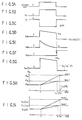
- Figs. 5A-5I show waveforms at the respective locations of Fig. 4.
- Fig. 6 is a flowchart illustrating double or multi-level programming of the present invention.
- the state of erasure means level zero, that is, the lowest level.
- the floating gate field effect transistor has an n-type channel formed on a p-type substrate.
- a floating gate field effect transistor in which a p-type channel is formed on a n-type substrate can be also employed. In this case, if the applied voltages are set to opposite polarities, and the signs of corresponding voltages and threshold voltages are reversed, the same operations can be performed as in the former case.
- V F,i (t) for the ith threshold level programming is applied to floating gate 31, and an inversion layer is formed in channel area 37 of field effect transistor 34. Because source 35, drain 36, and channel area 37 are located within a semiconductor substrate, when the inversion layer is formed, currents flow from drain 36 to source 35 through channel area 37. Voltages are supplied from third and fourth voltage sources 40 and 41 so that drain voltage V D and source voltage V S are induced to drain 36 and source 35, respectively.
- current I D,i (t) flows through drain 36.
- current I D,i (t) has its largest value at an initial stage, and decreases as programming proceeds because the electrons are injected to the floating gate to reduce the floating gate voltage.
- current detector 42 monitors drain current I D,i (t). When this value reaches threshold current Ith, as shown in Fig. 5E, the ith threshold level programming is completed and programming stop signal V ST is output, as shown in Fig. 5F.
- current detector 42 monitors current I D,i (t) at drain 36.
- the current detector 42 monitors the variation of the amount of voltage and charge at floating gate 31 during programming of Fig. 5D. Monitoring of current I D,i (t) can be regarded as monitoring the conductivity of the inversion layer formed in channel area 37.
- programming stop signal V ST is applied to first and second voltage sources 38 and 39.
- First and/or second voltage sources 38 and 39 stop supplying positive voltage V C,i and negative voltage V P to control gate 33 and program gate 32 in response to programming stop signal V ST , as shown in Figs. 5B and 5C.
- Time t P,i indicates when the ith threshold level is programmed.
- threshold current Ith is previously set as a value substantially corresponding to threshold voltage V F TH at floating gate 31.
- Threshold voltage V F TH at the floating gate is determined when the nonvolatile memory is fabricated, and can be defined at an arbitrary value of the threshold current Ith.
- threshold voltage V F TH substantially corresponds to the threshold voltage of channel area 37.
- the programming of any threshold level is completed when the floating gate voltage reaches threshold voltage V F TH . This is one feature that distinguishes the present invention from conventional technologies.
- Fig. 5H is a graph showing threshold voltages V C TH,1 and V C TH,2 at control gate 33, corresponding to the first and second threshold levels, respectively.
- threshold voltage V C TH,1 at control gate 33 increases as the programming level increases during the multi-level programming. This is performed by increasing voltage V C,i during programming.
- program times t P,1 and t P,2 of the first and second levels are different because the control gate voltage and threshold voltage shift of the respective levels are different.
- Fig. 5I is a graph showing the amount of charge variation at floating gate 31 from the initial charge amount Q F,0 (0) to the charge amount Q F,1 (t P,1 ) when the first threshold level programming is completed and to the charge amount Q F,2 (t P,2 ) when the second threshold level programming is completed, in the case where the ith threshold levels corresponds to the first and second levels.
- Fig. 5I is a graph showing the amount of charge variation at floating gate 31 from the initial charge amount Q F,0 (0) to the charge amount Q F,1 (t P,1 ) when the first threshold level programming is completed and to the charge amount Q F,2 (t P,2 ) when the second threshold level programming is completed, in the case where the ith threshold levels corresponds to the first and second levels.
- FIG. 7A the relationship between voltage V C,i applied to control gate 32 from first voltage source 38 and the threshold voltage at a corresponding level, which is a significant result of the present invention, will be explained.
- C C represents the capacitance between control gate 32 and floating gate
- C P represents the capacitance between program gate 32 and floating gate
- C D represents the capacitance between drain 36 and floating gate
- C S represents the capacitance between source 35 (including the substrate) and floating gate 31.
- equation (3) it is assumed that the source and substrate are grounded.
- the threshold voltage shift refers to a threshold voltage measured at the control gate and caused by the charges accumulated at the floating gate.
- Threshold voltage V C TH (t) measured at control gate 33 is defined as the voltage of control gate 33 when drain current I D (t) reaches threshold current Ith of current detector 42.
- Threshold current Ith can be defined arbitrarily as mentioned above. For instance, Ith can equal 1 ⁇ A.
- Threshold voltage V F TH at floating gate 31 is an inherent threshold voltage of the field effect transistor consisting of floating gate 31, source 35, and drain 36 of Fig. 3, which is determined by manufacturing conditions such as channel ion implantation and the thickness of a gate insulator in fabricating nonvolatile memory 100 of Fig. 3. Therefore, threshold voltage V F TH of floating gate 31 is always constant. Threshold voltage V C TH of control gate 33 is determined by the amount of charge Q F at floating gate 31.
- V 1 V F TH - ⁇ P V P - ⁇ D V D (t P ) ⁇ C
- V 1 V F TH - ⁇ P V P - ⁇ D V D (t P ) ⁇ C
- a corresponding level programming can be performed by applying to the control gate a voltage corresponding to the intended threshold level shift ⁇ V C TH,i added to the already known value V C,0 of the lowest level programming, and then waiting for the automatic completion of programming.
- tunnelling voltage V tun,i applied between floating gate 31 and program gate 32 for tunnelling is largest initially and smallest at a time point when voltage V F,i (t) reaches a given threshold voltage V F TH at floating gate 31, that is, when programming is completed.
- V max tun,i of the tunnelling voltage can be given as the following equation (9) by the difference between initial voltage V F,i (0) of floating gate 31 and voltage V P applied to program gate 32:
- equation (9) can be re-defined as the following equation (10):
- V max tun,i ⁇ C V C,i + ( ⁇ P - 1)V P + ⁇ D V D (0)
- the erasing process is very simple to describe. Erasure is performed in such a manner that voltages are applied to the respective parts to form, between the floating gate and source, drain, or channel area, electric fields strong enough to erase charge carriers accumulated at the floating gate. By doing so, the charge carriers are erased to the source, drain, or channel area through tunnelling.
- the erased state means the lowest threshold level, that is, V C TH,0 . In other words, all the nonvolatile memory cells within a given erasure block are programmed at the lowest level. Erasure is performed according to the following steps.
- threshold levels of the overall cells of a selected block are erased to become below level zero, that is, V C TH,0 .
- level zero that is, V C TH,0 .
- the overall selected cells are programmed.
- value V C,0 can be fixed arbitrarily. Erasure is performed substantially according to the programming method, thereby eliminating over-erasure problem.
- V C,i of control gate 33 and voltage V P of program gate 32 necessary for the ith threshold level programming are as follows.
- V C,i In order to monitor the charge variation of the floating gate during programming, voltage V C,i must be applied so that at the initial stage of programming, the channel of transistor shown in Fig. 4 is inverted to make the drain current flow, and during the programming, the conductivity of the inversion layer is reduced.
- the following equation (11) must be satisfied.
- V F,i (0) > V F TH , I D,i (0) > Ith Values V C,i and V P must be determined so that a tunnel electric field formed between program gate 32 and floating gate 31 to create tunnelling therebetween is strong enough for programming.
- Value V P is a fixed negative value so that the strength of the tunnel electric field increases as value V C,i becomes high.
- the speed of programming also increases as threshold voltage shift ⁇ V C TH of control gate 33 becomes large.
- the programming method in accordance with voltage detection is substantially the same as the programming in accordance with current detection.
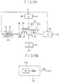
- Fig. 8 is a diagram for explaining the programming of the present invention using voltage detection.
- Fig. 8 is substantially the same as Fig. 4, aside from voltage detector 43 used instead of current detector 42 of Fig. 4.
- Voltage detector 43 can be made with a reference voltage source 44 and a resistor 45 connected between reference voltage source 44 and drain 36.
- the resistor 45 may be replace by a diode to form the voltage detector 43. This is the most simple configuration.
- Voltage detector 43 monitors the voltage of drain 36 during programming. During monitoring, when voltage V F,i of floating gate 31 reaches a threshold voltage V F TH , and if drain voltage V D,TH is detected, then a programming stop signal V ST is output. Value V D,TH is constant with respect to the overall programming level.
- programming is completed when, in response to programming stop signal V ST , first and/or second voltage sources 38 and 39 cut off control gate voltage V C,i and program gate voltage V P .
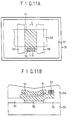
- a first structure of a nonvolatile memory of the present invention comprises a first conductivity-type semiconductor substrate 50 having a channel area on its surface, floating gate 51 formed on the channel area, control gate 52 formed above floating gate 51, program gate 53 formed adjacent to floating gate 51, and an insulating layer 54 formed between program gate 53, floating gate 51, and control gate 52.
- the insulating layer 54 is sufficiently thin between floating gate 51 and program gate 53 to enable tunnelling therebetween.
- a field insulating layer 55 is formed on the surface of substrate 50 surrounding the channel area. Part of floating gate 51 extends to the surface of field insulating layer 55.
- program gate 53 is placed adjacent to one side of control gate 52.
- a gate insulating layer 56 is formed sufficiently thin to enable tunnelling between the channel area and floating gate 51.
- a second structure of the present invention is similar to that of the first structure.
- part of program gate 53 is placed adjacent to the bottom of floating gate 51.
- a third structure of the present invention again is similar to that of the first structure.
- program gate 53 is placed adjacent to the top of floating gate 51.
- a fourth structure of nonvolatile memory of the present invention comprises a first conductivity-type semiconductor substrate 50 having a channel area on its surface, floating gate 51 formed on the channel area, two second conductivity-type impurity areas 57 and 58 formed on either side of the channel area within the surface of the semiconductor substrate, control gate 52 formed above floating gate 51, program gate 53 formed adjacent to floating gate 51, and an insulating layer 54 formed between program gate 53, floating gate 51, and control gate 52.
- the insulating layer 54 is sufficiently thin between floating gate 51 and program gate 53 to enable tunnelling therebetween.
- a field insulating layer 55 surrounds the channel region.
- a gate insulating film 56 is formed sufficiently thin to enable tunnelling between the channel area and the floating gate 51.
- the nonvolatile memory device of the present invention comprises a semiconductor substrate 60, a plurality of word lines 61 spaced apart by a predetermined distance on substrate 60, a plurality of bit lines 62 perpendicular to the word lines to form a plurality of squares or rectangles spaced apart by a predetermined distance, a plurality of program lines 63 disposed in the same direction as the respective bit lines, and a plurality of nonvolatile memory cells 64 disposed in each of the respective squares or rectangles.
- nonvolatile memory cells 64 each comprise a floating gate 65, program gate 66 for supplying charges to floating gate 65 for the purpose of programming, control gate 67 for controlling the amount of charges supplied to floating gate 65 for the purpose of programming, and field effect transistor 68 for reading (or verifying) the amount of charge carriers supplied to floating gate 65 during programming.
- Field effect transistor 68 is composed of floating gate 65, source 69, drain 70, and channel area 71 between source 69 and drain 70.
- Control gate 67 of the respective memory cells is connected to nearby word line 61 and program gate 66 is connected to nearby program line 63.
- Source 69 of nonvolatile memory cell 64 is commonly connected to nearby bit line 62 along with drain 70 of nonvolatile memory cell 64 placed in a nearby or adjacent square.
- - 8- - 15V is applied to a selected program line 63, 0V to unselected program lines 63, 3-12V to a selected word line 61, 0- - 10V to unselected word lines 61, 0.5-2V to a selected bit line 62, 0V to unselected bit lines 62 placed to the left, for example, of a selected cell, 0.5-2V to more than one bit line placed to the right, for example, of the selected cell, and 0V to substrate 60.
- 0- - 12V is applied to the overall program lines 63 of a selected erasure block, - 7- - 12V to the overall word lines 61 of the selected erasure block, 0-6V to the overall bit lines 61 of the selected erasure block, and 0V to substrate 60.
- 0- - 12V is applied to the overall program lines 63 of a selected erasure block, - 7- - 12V to the overall word lines 61 of the selected erasure block.
- Bit lines 62 of the selected block are floated.
- 0-6V is applied to substrate 60.
- 0V is applied to program lines 63, Power supply voltage Vcc to a selected word line 61, 0V to unselected word lines 61, 0.5-2V to a selected bit line 62, 0V to unselected bit lines 62 placed to the left, for example, 0.5-2V to bit lines 62 placed right, for example, of the selected cell, and 0V to substrate 60.
- the voltages of Fig. 13B can be varied with structural characteristics or electrical parameters of the memory cells, for instance, the coupling coefficient or the thickness of tunnel insulator.
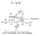
- the nonvolatile memory comprises a floating gate 81 divided into a first area 81a and a second area 81b; a programming field effect transistor including first area 81a of floating gate 81, first drain 82, and common source 83, channel region between the first drain 82 and the common source 83 and having a first threshold voltage V F TH1 for supplying charge carriers to floating gate 81 for the purpose of programming; a control gate 84 for providing voltage to floating gate by capacitive coupling between floating gate and control gate and controlling the amount of charge carriers supplied to floating gate 81 for programming; and a monitoring field effect transistor including second area 81b of floating gate 81 (excluding first area 81a), second drain 85, and common source 83, channel region between the second drain 85 and the common source 83 and having a second threshold voltage V F TH2 for verifying the amount of charge carriers supplied to floating gate 81 during programming.
- second threshold voltage V F TH2 must be greater than first threshold voltage V F TH1
- the second embodiment of nonvolatile memory cell of the present invention does not have a program gate, and instead has three impurity areas (the drain of the monitoring transistor, common source, and the drain of the programming transistor) on the surface of the substrate.
- the memory of Fig. 15A further comprises a first voltage source 88 for supplying a voltage to control gate 84, a second voltage source 89 for supplying a voltage V P D to first drain 82 of the programming field effect transistor for programming, a third voltage source 90 for supplying to common source 83 a voltage V S lower than or equal to voltage V P D supplied to first drain 82, and a current detector 91A for detecting current I D,i (t) flowing through second drain 85 of the monitoring field effect transistor during programming and supplying programming stop signal V ST to respective voltage sources 88, 89 and 90 when the detected current reaches a set threshold current Ith to cut off voltages V C,i , V P D , and V S .
- common source 83 is grounded with the substrate (not shown).
- voltage V C,i supplied to control gate 84 from first voltage source 88 is a positive voltage varying in correspondence with the respective threshold level programming of the multi-level programming.
- Voltage V P D supplied to the programming field effect transistor from second voltage source 89 is a positive voltage.
- Current detector 91A of Fig. 15A can be replaced with voltage detector 91B of Fig. 15B.
- the nonvolatile memory cell further comprises a first voltage source 88 for supplying a voltage V C,i to control gate 84, a second voltage source 89 for supplying a voltage V P D to first drain 82 of the programming field effect transistor for programming, a third voltage source 90 for supplying to common source 83 a voltage V S lower than or equal to voltage V P D supplied to first drain 82, and a voltage detector 91B for monitoring voltage V M D,i (t) during programming and supplying programming stop signal V ST to the first and second voltage sources 88 and 89 when the monitored voltage V M D,i (t) of second drain 85 reaches a set reference voltage V D,TH to cut off voltages V C,i and V P D .
- a first voltage source 88 for supplying a voltage V C,i to control gate 84
- a second voltage source 89 for supplying a voltage V P D to first drain 82 of the programming field effect transistor for programming
- a third voltage source 90 for supplying to common source 83 a voltage
- voltage V C,i supplied to control gate 84 from first voltage source 88 is a positive voltage varying in correspondence with the respective threshold level programming of the multi-level programming.
- Voltage V P D supplied to first drain 82 of the programming field effect transistor from second voltage source 89 is a positive voltage in case of programming using hot carrier injection mechanism.
- voltage detector 91B can be configured with a voltage source V DD for inducing a voltage at second drain 85, and a resistor connected between voltage source V DD and second drain 85 of the monitoring field effect transistor.
- Voltage V P is set to be less than or equal to zero ( ⁇ 0) and is supplied to the program gate of the first embodiment shown in Figs. 3B and 4.
- the cell of the second embodiment shown in Figs. 15A and 15B uses a programming field effect transistor instead of the program gate.
- a method of programming the second embodiment of the nonvolatile memory cell of the present invention includes the steps of: supplying first voltage V C,i to control gate 84 and second voltage V P D to first drain 82 so that charge carriers are fed to floating gate 81 through first channel area 86 for programming and an inversion layer is formed in second channel area 87; and monitoring the conductivity of the inversion layer during programming and cutting off the supply of
- supplying charge carriers to floating gate 81 from first channel area 86 for programming can be performed through hot carrier injection or Fowler-Norheim (FN) tunnelling.
- FN Fowler-Norheim
- the voltage applied to the first drain is less than or equal to zero, and the voltage applied to the common source is equal to that or the first drain.
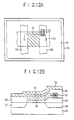
- the nonvolatile memory cell comprises a first conductivity-type (P type) semiconductor substrate 92, a second conductivity-type (n+) first impurity area 93, second impurity area 94, and third impurity area 95 sequentially formed on the surface of substrate 92 while spaced apart by a predetermined distance, a first gate insulating layer 98 formed over first and second impurity areas 93 and 94 on substrate 92, a second gate insulating layer 99 formed over second impurity area 94 and third impurity area 95 and having a different thickness from that of first gate insulating layer 98, a first channel area 100 defined as a region between first and second impurity areas 93 and 94 on the surface of substrate 92, a second channel area 101 defined as a region between second and third impurity areas 94 and 95 on the surface of substrate 92, a floating gate 96 formed over first and third impurity areas 93 and 95 on first and second gate insulating layers
- second gate insulating layer 99 is thicker than first gate insulating layer 98.
- First gate insulating layer 98 is determined to be sufficiently thin so that charge carriers are erased to first channel area 100 from floating gate 96 through tunnelling.
- a field insulating layer 103 is further formed on the surface of substrate 92 excluding first gate insulating layer 98 and second gate insulating layer 99.
- floating gate 96 is formed over first and second channel areas 100 and 101. Part of floating gate 96 extends to the surface of field insulating layer 103.
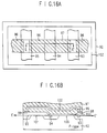
- the nonvolatile memory device of the present invention comprises a plurality of word lines 104 disposed to be spaced apart by a predetermined distance, a plurality of second conductivity-type bit lines 105 disposed to be perpendicular to word lines 104 to form a plurality of squares or rectangles spaced apart by a predetermined distance, common source lines 106 formed to divide the respective squares or rectangles in the same direction as bit lines 105 into the left and right areas between bit lines 105, and a plurality of nonvolatile memory cells having a control gate 84, a floating gate 81 divided into, first and second areas 81a and 81b, a programming field effect transistor placed to the right of the squares, for example, and for supplying charge carriers to floating gate 81 for programming, and a monitoring field effect transistor placed to the left of the squares, for example, and for verifying the amount of charge carriers of floating gate 81 during programming.
- the programming field effect transistor includes first area 81a of floating gate 81, a first drain 82, and common source 83, and a first channel area 86 placed between first drain 82 and common source 83.
- the monitoring field effect transistor includes second area 81b of floating gate 81, a second drain 85, and common source 83, and a second channel area 87 placed between second drain 85 and common source 83.
- the control gate 84 is connected to nearby word line 104, and the common source 83 is connected to common source line 106.
- the first drain 82 is connected to nearby bit line 105 together with second drain 85 of the nonvolatile memory located in a square to the right of the first drain, for example, and the second drain 85 is connected to first drain 82 of the nonvolatile memory located in a square to the left of the second drain 85, for example.
- Fig. 17A When the nonvolatile memory device of Fig. 17A operates in the program mode using the hot carrier injection mechanism.
- 6-13V can be applied to a selected word line, 0V to unselected word line, 5-9V to a selected n th bit line, 0.5-2V to a selected (n-1) th bit lines, 0V to other bit lines, 0V to a selected n th source line, an unselected (n+1) th source line is floated, an unselected (n-1) th source line is equal to a selected (n-1) th bit line, and 0V to the substrate.
- 10-20V is applied to a selected word line, 0V to an unselected word line, 0V to a selected n th bit line, 5-10V to other bit lines, 0V to a selected n th source line, 5-10V to other source lines, and 0V to substrate.
- -7 to -12V can be applied to a selected word line and an unselected word line, all bit lines are floated, Vcc is applied to all source lines, and 0V to the substrate.
- Vcc can be applied to a selected word line, 0V to an unselected word line, 0.5 to 2V to a selected n th bit line, 0V to other bit lines, 0V to all source lines, and 0V to the substrate.
- the voltages of Fig. 17B can be varied with structural characteristics or electrical parameters of the memory cells, for instance, the coupling coefficient or the thickness of tunnel insulator.
- the present invention is advantageous in the following respects.
- respective threshold level programming is accomplished merely by changing the voltage of the control gate thereby, facilitating multi-level programming.
- the respective threshold voltage levels and corresponding control gate voltages are linear, and the shift of the threshold voltage coincides with the shift of the control gate voltage, precisely adjusting the shift of the respective level threshold voltages.
- the state of erasure is controlled by the lowest level programming at an arbitrary control gate voltage, thereby eliminating over-erasure problem.
- pre-programming is not necessary prior to erasure.
- a small voltage below ⁇ 12V is required for operation.
- Seventh, only a small current below several or tens of ⁇ A is merely required for verification.
- the nonvolatile memory cell is constructed as a simple-stacked gate, not a split-channel, making it compact.
- the accuracy of multi-level programming that is, the error distribution of programmed threshold voltages is precisely determined only by parameters fixed at the time of fabrication of the nonvolatile memory and by applied bias voltages. For this reason, the error distribution of the respective levels of the nonvolatile memory of the present invention is not dependent on the large number of program/erase cycles. Even during programming, the memory is not dependent on the trap of charges to the oxide layer, channel mobility, bit line resistance, and unstable or unpredictable electric elements.
- the programming method of the nonvolatile memory of the present invention is voltage-controlled, performing easier and more precise multi-level programming than the current-controlled method.
- the nonvolatile memory device of the present invention accomplishes a contactless virtual ground array with a simple stacked-gate structure not an asymmetric cell like the split-channel structure, sharply reducing the size of chip.
- the source and drain of the nonvolatile memory of the present invention are used only in reading, applying a low voltage required only for reading to the source and drain. This optimizes the diffusion area of the source and drain.
Landscapes
- Engineering & Computer Science (AREA)
- Microelectronics & Electronic Packaging (AREA)
- Computer Hardware Design (AREA)
- Read Only Memory (AREA)
- Non-Volatile Memory (AREA)
- Semiconductor Memories (AREA)
Applications Claiming Priority (2)
| Application Number | Priority Date | Filing Date | Title |
|---|---|---|---|
| KR1019950025761A KR100192430B1 (ko) | 1995-08-21 | 1995-08-21 | 비휘발성 메모리 및 이 비휘발성 메모리를 프로그램하는 방법 |
| KR2576195 | 1995-08-21 |
Publications (3)
| Publication Number | Publication Date |
|---|---|
| EP0759622A2 true EP0759622A2 (de) | 1997-02-26 |
| EP0759622A3 EP0759622A3 (de) | 1998-10-21 |
| EP0759622B1 EP0759622B1 (de) | 2001-11-07 |
Family
ID=19423947
Family Applications (1)
| Application Number | Title | Priority Date | Filing Date |
|---|---|---|---|
| EP96113258A Expired - Lifetime EP0759622B1 (de) | 1995-08-21 | 1996-08-19 | Nichtflüchtiger Speicher und Verfahren zu seiner Programmierung |
Country Status (10)
| Country | Link |
|---|---|
| US (2) | US5745412A (de) |
| EP (1) | EP0759622B1 (de) |
| JP (1) | JP2932424B2 (de) |
| KR (1) | KR100192430B1 (de) |
| CN (1) | CN1107322C (de) |
| DE (1) | DE69616693T2 (de) |
| MY (1) | MY119029A (de) |
| RU (1) | RU2111556C1 (de) |
| SG (1) | SG50754A1 (de) |
| TW (1) | TW279984B (de) |
Cited By (2)
| Publication number | Priority date | Publication date | Assignee | Title |
|---|---|---|---|---|
| FR2879338A1 (fr) * | 2004-12-14 | 2006-06-16 | St Microelectronics Sa | Cellule memoire eeprom comprenant une fenetre tunnel deportee |
| DE19822523B4 (de) * | 1997-05-26 | 2008-03-13 | LG Semicon Co., Ltd., Cheongju | Nichtflüchtige Halbleiter-Speicherzelle, nichtflüchtiges Halbleiterspeicher-Bauteil und Verfahren zum Herstellen eines nichtflüchtigen Halbleiterspeicher-Bauteils |
Families Citing this family (31)
| Publication number | Priority date | Publication date | Assignee | Title |
|---|---|---|---|---|
| KR100205309B1 (ko) | 1996-07-23 | 1999-07-01 | 구본준 | 비휘발성 메모리셀 및 이 비휘발성 메모리셀을 프로그래밍하는 방법 |
| KR100232190B1 (ko) * | 1996-10-01 | 1999-12-01 | 김영환 | 비휘발성 메모리장치 |
| KR100327421B1 (ko) * | 1997-12-31 | 2002-07-27 | 주식회사 하이닉스반도체 | 비휘발성 메모리 소자의 프로그램 시스템 및 그의 프로그램 방법 |
| US6088268A (en) * | 1998-09-17 | 2000-07-11 | Atmel Corporation | Flash memory array with internal refresh |
| KR100283909B1 (ko) | 1998-12-15 | 2001-03-02 | 김영환 | 비휘발성 메모리의 전하 이득 스트레스 테스트 회로 및 그 테스트 방법 |
| US6901006B1 (en) | 1999-07-14 | 2005-05-31 | Hitachi, Ltd. | Semiconductor integrated circuit device including first, second and third gates |
| JP4012341B2 (ja) | 1999-07-14 | 2007-11-21 | 株式会社ルネサステクノロジ | 半導体集積回路装置 |
| US6172914B1 (en) * | 1999-08-13 | 2001-01-09 | Advanced Micro Devices, Inc. | Concurrent erase verify scheme for flash memory applications |
| JP2001148434A (ja) * | 1999-10-12 | 2001-05-29 | New Heiro:Kk | 不揮発性メモリセルおよびその使用方法、製造方法ならびに不揮発性メモリアレイ |
| US6531887B2 (en) | 2001-06-01 | 2003-03-11 | Macronix International Co., Ltd. | One cell programmable switch using non-volatile cell |
| US6545504B2 (en) * | 2001-06-01 | 2003-04-08 | Macronix International Co., Ltd. | Four state programmable interconnect device for bus line and I/O pad |
| US6577161B2 (en) | 2001-06-01 | 2003-06-10 | Macronix International Co., Ltd. | One cell programmable switch using non-volatile cell with unidirectional and bidirectional states |
| US6522584B1 (en) * | 2001-08-02 | 2003-02-18 | Micron Technology, Inc. | Programming methods for multi-level flash EEPROMs |
| US20050102573A1 (en) * | 2003-11-03 | 2005-05-12 | Macronix International Co., Ltd. | In-circuit configuration architecture for embedded configurable logic array |
| US20050097499A1 (en) * | 2003-11-03 | 2005-05-05 | Macronix International Co., Ltd. | In-circuit configuration architecture with non-volatile configuration store for embedded configurable logic array |
| US7466590B2 (en) * | 2004-02-06 | 2008-12-16 | Sandisk Corporation | Self-boosting method for flash memory cells |
| US7161833B2 (en) * | 2004-02-06 | 2007-01-09 | Sandisk Corporation | Self-boosting system for flash memory cells |
| US7009887B1 (en) * | 2004-06-03 | 2006-03-07 | Fasl Llc | Method of determining voltage compensation for flash memory devices |
| US7663167B2 (en) * | 2004-12-23 | 2010-02-16 | Aptina Imaging Corp. | Split transfer gate for dark current suppression in an imager pixel |
| US7428165B2 (en) * | 2006-03-30 | 2008-09-23 | Sandisk Corporation | Self-boosting method with suppression of high lateral electric fields |
| US7511995B2 (en) * | 2006-03-30 | 2009-03-31 | Sandisk Corporation | Self-boosting system with suppression of high lateral electric fields |
| US7907450B2 (en) * | 2006-05-08 | 2011-03-15 | Macronix International Co., Ltd. | Methods and apparatus for implementing bit-by-bit erase of a flash memory device |
| US20090135640A1 (en) * | 2007-11-28 | 2009-05-28 | International Business Machines Corporation | Electromigration-programmable semiconductor device with bidirectional resistance change |
| US7808833B2 (en) * | 2008-01-28 | 2010-10-05 | Qimonda Flash Gmbh | Method of operating an integrated circuit, integrated circuit and method to determine an operating point |
| CN101872648B (zh) * | 2009-04-23 | 2013-04-24 | 上海华虹Nec电子有限公司 | Mos一次可编程器件 |
| JP2010267341A (ja) * | 2009-05-15 | 2010-11-25 | Renesas Electronics Corp | 半導体装置 |
| RU2436176C2 (ru) * | 2009-09-04 | 2011-12-10 | Корпорация "САМСУНГ ЭЛЕКТРОНИКС Ко., Лтд." | Способ определения тока и вращательного момента в многослойной структуре в приближении сильной связи |
| US8384147B2 (en) * | 2011-04-29 | 2013-02-26 | Silicon Storage Technology, Inc. | High endurance non-volatile memory cell and array |
| US9543021B2 (en) * | 2014-03-12 | 2017-01-10 | SK Hynix Inc. | Semiconductor device and programming method thereof |
| US12198770B2 (en) | 2022-11-17 | 2025-01-14 | Macronix International Co., Ltd. | Memory device for increasing speed of soft-program operation |
| TWI852173B (zh) * | 2022-11-17 | 2024-08-11 | 旺宏電子股份有限公司 | 記憶體裝置 |
Family Cites Families (28)
| Publication number | Priority date | Publication date | Assignee | Title |
|---|---|---|---|---|
| US4331968A (en) * | 1980-03-17 | 1982-05-25 | Mostek Corporation | Three layer floating gate memory transistor with erase gate over field oxide region |
| JPS5798190A (en) * | 1980-12-08 | 1982-06-18 | Toshiba Corp | Semiconductor storage device |
| US4558344A (en) * | 1982-01-29 | 1985-12-10 | Seeq Technology, Inc. | Electrically-programmable and electrically-erasable MOS memory device |
| EP0100772B1 (de) * | 1982-08-06 | 1987-11-19 | Deutsche ITT Industries GmbH | Elektrisch programmierbare Speichermatrix |
| JPS60236195A (ja) * | 1984-05-08 | 1985-11-22 | Nec Corp | 不揮発性半導体メモリ |
| FR2600809B1 (fr) * | 1986-06-24 | 1988-08-19 | Eurotechnique Sa | Dispositif de detection du fonctionnement du systeme de lecture d'une cellule-memoire eprom ou eeprom |
| JPS63274180A (ja) * | 1987-05-06 | 1988-11-11 | Seiko Instr & Electronics Ltd | 半導体不揮発性メモリ |
| JPS63310179A (ja) * | 1987-06-12 | 1988-12-19 | Seiko Instr & Electronics Ltd | 半導体不揮発性メモリ− |
| US5268318A (en) * | 1988-06-08 | 1993-12-07 | Eliyahou Harari | Highly compact EPROM and flash EEPROM devices |
| US5043940A (en) * | 1988-06-08 | 1991-08-27 | Eliyahou Harari | Flash EEPROM memory systems having multistate storage cells |
| FR2635410B1 (fr) * | 1988-08-11 | 1991-08-02 | Sgs Thomson Microelectronics | Memoire de type eprom a haute densite d'integration avec une organisation en damier et un facteur de couplage ameliore et procede de fabrication |
| US5216269A (en) * | 1989-03-31 | 1993-06-01 | U.S. Philips Corp. | Electrically-programmable semiconductor memories with buried injector region |
| JPH02260298A (ja) * | 1989-03-31 | 1990-10-23 | Oki Electric Ind Co Ltd | 不揮発性多値メモリ装置 |
| US5081054A (en) * | 1989-04-03 | 1992-01-14 | Atmel Corporation | Fabrication process for programmable and erasable MOS memory device |
| US5163021A (en) * | 1989-04-13 | 1992-11-10 | Sundisk Corporation | Multi-state EEprom read and write circuits and techniques |
| US5187683A (en) * | 1990-08-31 | 1993-02-16 | Texas Instruments Incorporated | Method for programming EEPROM memory arrays |
| US5282161A (en) * | 1990-12-31 | 1994-01-25 | Sgs-Thomson Microelectronics S.R.L. | Eeprom cell having a read interface isolated from the write/erase interface |
| US5218569A (en) * | 1991-02-08 | 1993-06-08 | Banks Gerald J | Electrically alterable non-volatile memory with n-bits per memory cell |
| US5264384A (en) * | 1991-08-30 | 1993-11-23 | Texas Instruments Incorporated | Method of making a non-volatile memory cell |
| US5467305A (en) * | 1992-03-12 | 1995-11-14 | International Business Machines Corporation | Three-dimensional direct-write EEPROM arrays and fabrication methods |
| US5386132A (en) * | 1992-11-02 | 1995-01-31 | Wong; Chun C. D. | Multimedia storage system with highly compact memory device |
| JPH06251590A (ja) * | 1993-02-24 | 1994-09-09 | Hitachi Ltd | 半導体集積回路装置 |
| US5329487A (en) * | 1993-03-08 | 1994-07-12 | Altera Corporation | Two transistor flash EPROM cell |
| JPH06334195A (ja) * | 1993-05-18 | 1994-12-02 | Nippon Steel Corp | 不揮発性半導体記憶装置 |
| US5422842A (en) * | 1993-07-08 | 1995-06-06 | Sundisk Corporation | Method and circuit for simultaneously programming and verifying the programming of selected EEPROM cells |
| US5357466A (en) * | 1993-07-14 | 1994-10-18 | United Microelectronics Corporation | Flash cell with self limiting erase and constant cell current |
| DE69433001T2 (de) * | 1993-10-12 | 2004-06-17 | Texas Instruments Inc., Dallas | Niederspannungs-Flash-EEPROM-X-Zelle mit Fowler-Nordheim-Tunneling |
| JP2937805B2 (ja) * | 1995-05-19 | 1999-08-23 | モトローラ株式会社 | 2層フローティングゲート構造のマルチビット対応セルを有する不揮発性メモリ及びそのプログラム/消去/読出方法 |
-
1995
- 1995-08-21 KR KR1019950025761A patent/KR100192430B1/ko not_active Expired - Fee Related
- 1995-09-29 US US08/537,327 patent/US5745412A/en not_active Expired - Lifetime
- 1995-11-02 TW TW084111579A patent/TW279984B/zh not_active IP Right Cessation
-
1996
- 1996-01-17 MY MYPI96000170A patent/MY119029A/en unknown
- 1996-01-24 RU RU96101896A patent/RU2111556C1/ru not_active IP Right Cessation
- 1996-02-16 JP JP8052595A patent/JP2932424B2/ja not_active Expired - Fee Related
- 1996-04-11 CN CN96102817A patent/CN1107322C/zh not_active Expired - Fee Related
- 1996-08-19 DE DE69616693T patent/DE69616693T2/de not_active Expired - Lifetime
- 1996-08-19 EP EP96113258A patent/EP0759622B1/de not_active Expired - Lifetime
- 1996-08-21 SG SG1996010503A patent/SG50754A1/en unknown
-
1998
- 1998-03-13 US US09/042,022 patent/US5905674A/en not_active Expired - Lifetime
Cited By (2)
| Publication number | Priority date | Publication date | Assignee | Title |
|---|---|---|---|---|
| DE19822523B4 (de) * | 1997-05-26 | 2008-03-13 | LG Semicon Co., Ltd., Cheongju | Nichtflüchtige Halbleiter-Speicherzelle, nichtflüchtiges Halbleiterspeicher-Bauteil und Verfahren zum Herstellen eines nichtflüchtigen Halbleiterspeicher-Bauteils |
| FR2879338A1 (fr) * | 2004-12-14 | 2006-06-16 | St Microelectronics Sa | Cellule memoire eeprom comprenant une fenetre tunnel deportee |
Also Published As
| Publication number | Publication date |
|---|---|
| DE69616693D1 (de) | 2001-12-13 |
| DE69616693T2 (de) | 2002-07-25 |
| JPH0964214A (ja) | 1997-03-07 |
| US5745412A (en) | 1998-04-28 |
| EP0759622B1 (de) | 2001-11-07 |
| RU2111556C1 (ru) | 1998-05-20 |
| US5905674A (en) | 1999-05-18 |
| CN1143814A (zh) | 1997-02-26 |
| EP0759622A3 (de) | 1998-10-21 |
| JP2932424B2 (ja) | 1999-08-09 |
| SG50754A1 (en) | 1998-07-20 |
| MY119029A (en) | 2005-03-31 |
| TW279984B (en) | 1996-07-01 |
| CN1107322C (zh) | 2003-04-30 |
| KR100192430B1 (ko) | 1999-06-15 |
Similar Documents
| Publication | Publication Date | Title |
|---|---|---|
| EP0759622B1 (de) | Nichtflüchtiger Speicher und Verfahren zu seiner Programmierung | |
| US6411547B2 (en) | Nonvolatile memory cell and method for programming and/or verifying the same | |
| US5801993A (en) | Nonvolatile memory device | |
| US6172397B1 (en) | Non-volatile semiconductor memory device | |
| KR100260070B1 (ko) | 개선된 트랜지스터 셀을 포함하는 플래시 메모리 및 그 메모리를 프로그래밍하는 방법 | |
| US5544103A (en) | Compact page-erasable eeprom non-volatile memory | |
| EP1638110B1 (de) | Verfahren und Vorrichtung zum Betreiben einer Kette von Ladungshaftstellen-Speicherzellen | |
| US7483307B2 (en) | Method and apparatus for sensing in charge trapping non-volatile memory | |
| EP0080560B1 (de) | Speicherzelle mit schwebendem Gatter | |
| EP0646933A2 (de) | Verfahren zum Programmieren von Schwebendengatterspeicherzellen | |
| US20110121380A1 (en) | Non-volatile electrically alterable memory cell for storing multiple data | |
| EP0763829A2 (de) | Verfahren zum programmieren eines nichflüchtigen Speicher | |
| US7072219B1 (en) | Method and apparatus for operating a non-volatile memory array | |
| WO1992013349A1 (en) | Single transistor eeprom architecture | |
| US7130215B2 (en) | Method and apparatus for operating a non-volatile memory device | |
| US5394357A (en) | Non-volatile semiconductor memory device | |
| EP0463331A2 (de) | Verbessertes Verfahren zur Programmierung eines nichtflüchtigen Speichers | |
| US7072220B1 (en) | Method and apparatus for operating a non-volatile memory array |
Legal Events
| Date | Code | Title | Description |
|---|---|---|---|
| PUAI | Public reference made under article 153(3) epc to a published international application that has entered the european phase |
Free format text: ORIGINAL CODE: 0009012 |
|
| AK | Designated contracting states |
Kind code of ref document: A2 Designated state(s): DE FR GB NL |
|
| PUAL | Search report despatched |
Free format text: ORIGINAL CODE: 0009013 |
|
| AK | Designated contracting states |
Kind code of ref document: A3 Designated state(s): DE FR GB NL |
|
| 17P | Request for examination filed |
Effective date: 19990416 |
|
| 17Q | First examination report despatched |
Effective date: 20000321 |
|
| GRAG | Despatch of communication of intention to grant |
Free format text: ORIGINAL CODE: EPIDOS AGRA |
|
| GRAG | Despatch of communication of intention to grant |
Free format text: ORIGINAL CODE: EPIDOS AGRA |
|
| GRAH | Despatch of communication of intention to grant a patent |
Free format text: ORIGINAL CODE: EPIDOS IGRA |
|
| GRAH | Despatch of communication of intention to grant a patent |
Free format text: ORIGINAL CODE: EPIDOS IGRA |
|
| GRAA | (expected) grant |
Free format text: ORIGINAL CODE: 0009210 |
|
| AK | Designated contracting states |
Kind code of ref document: B1 Designated state(s): DE FR GB NL |
|
| REF | Corresponds to: |
Ref document number: 69616693 Country of ref document: DE Date of ref document: 20011213 |
|
| REG | Reference to a national code |
Ref country code: GB Ref legal event code: IF02 |
|
| ET | Fr: translation filed | ||
| PLBE | No opposition filed within time limit |
Free format text: ORIGINAL CODE: 0009261 |
|
| STAA | Information on the status of an ep patent application or granted ep patent |
Free format text: STATUS: NO OPPOSITION FILED WITHIN TIME LIMIT |
|
| 26N | No opposition filed | ||
| PGFP | Annual fee paid to national office [announced via postgrant information from national office to epo] |
Ref country code: GB Payment date: 20120724 Year of fee payment: 17 |
|
| PGFP | Annual fee paid to national office [announced via postgrant information from national office to epo] |
Ref country code: DE Payment date: 20120724 Year of fee payment: 17 Ref country code: FR Payment date: 20120808 Year of fee payment: 17 |
|
| PGFP | Annual fee paid to national office [announced via postgrant information from national office to epo] |
Ref country code: NL Payment date: 20120724 Year of fee payment: 17 |
|
| REG | Reference to a national code |
Ref country code: NL Ref legal event code: V1 Effective date: 20140301 |
|
| GBPC | Gb: european patent ceased through non-payment of renewal fee |
Effective date: 20130819 |
|
| PG25 | Lapsed in a contracting state [announced via postgrant information from national office to epo] |
Ref country code: NL Free format text: LAPSE BECAUSE OF NON-PAYMENT OF DUE FEES Effective date: 20140301 Ref country code: DE Free format text: LAPSE BECAUSE OF NON-PAYMENT OF DUE FEES Effective date: 20140301 |
|
| REG | Reference to a national code |
Ref country code: DE Ref legal event code: R119 Ref document number: 69616693 Country of ref document: DE Effective date: 20140301 |
|
| REG | Reference to a national code |
Ref country code: FR Ref legal event code: ST Effective date: 20140430 |
|
| PG25 | Lapsed in a contracting state [announced via postgrant information from national office to epo] |
Ref country code: GB Free format text: LAPSE BECAUSE OF NON-PAYMENT OF DUE FEES Effective date: 20130819 |
|
| PG25 | Lapsed in a contracting state [announced via postgrant information from national office to epo] |
Ref country code: FR Free format text: LAPSE BECAUSE OF NON-PAYMENT OF DUE FEES Effective date: 20130902 |