EP0759638A2 - Halbleiterbauelement mit hoher Spannungsfestigkeit und dessen Herstellungsverfahren - Google Patents
Halbleiterbauelement mit hoher Spannungsfestigkeit und dessen Herstellungsverfahren Download PDFInfo
- Publication number
- EP0759638A2 EP0759638A2 EP96104778A EP96104778A EP0759638A2 EP 0759638 A2 EP0759638 A2 EP 0759638A2 EP 96104778 A EP96104778 A EP 96104778A EP 96104778 A EP96104778 A EP 96104778A EP 0759638 A2 EP0759638 A2 EP 0759638A2
- Authority
- EP
- European Patent Office
- Prior art keywords
- diffusion region
- impurity diffusion
- conductivity type
- withstand voltage
- layer
- Prior art date
- Legal status (The legal status is an assumption and is not a legal conclusion. Google has not performed a legal analysis and makes no representation as to the accuracy of the status listed.)
- Granted
Links
Images











Classifications
-
- H—ELECTRICITY
- H10—SEMICONDUCTOR DEVICES; ELECTRIC SOLID-STATE DEVICES NOT OTHERWISE PROVIDED FOR
- H10D—INORGANIC ELECTRIC SEMICONDUCTOR DEVICES
- H10D30/00—Field-effect transistors [FET]
- H10D30/60—Insulated-gate field-effect transistors [IGFET]
- H10D30/64—Double-diffused metal-oxide semiconductor [DMOS] FETs
- H10D30/65—Lateral DMOS [LDMOS] FETs
- H10D30/657—Lateral DMOS [LDMOS] FETs having substrates comprising insulating layers, e.g. SOI-LDMOS transistors
-
- H—ELECTRICITY
- H10—SEMICONDUCTOR DEVICES; ELECTRIC SOLID-STATE DEVICES NOT OTHERWISE PROVIDED FOR
- H10D—INORGANIC ELECTRIC SEMICONDUCTOR DEVICES
- H10D12/00—Bipolar devices controlled by the field effect, e.g. insulated-gate bipolar transistors [IGBT]
- H10D12/411—Insulated-gate bipolar transistors [IGBT]
-
- H—ELECTRICITY
- H10—SEMICONDUCTOR DEVICES; ELECTRIC SOLID-STATE DEVICES NOT OTHERWISE PROVIDED FOR
- H10D—INORGANIC ELECTRIC SEMICONDUCTOR DEVICES
- H10D12/00—Bipolar devices controlled by the field effect, e.g. insulated-gate bipolar transistors [IGBT]
- H10D12/411—Insulated-gate bipolar transistors [IGBT]
- H10D12/421—Insulated-gate bipolar transistors [IGBT] on insulating layers or insulating substrates, e.g. thin-film IGBTs
-
- H—ELECTRICITY
- H10—SEMICONDUCTOR DEVICES; ELECTRIC SOLID-STATE DEVICES NOT OTHERWISE PROVIDED FOR
- H10D—INORGANIC ELECTRIC SEMICONDUCTOR DEVICES
- H10D18/00—Thyristors
- H10D18/60—Gate-turn-off devices
- H10D18/65—Gate-turn-off devices with turn-off by field effect
- H10D18/655—Gate-turn-off devices with turn-off by field effect produced by insulated gate structures
-
- H—ELECTRICITY
- H10—SEMICONDUCTOR DEVICES; ELECTRIC SOLID-STATE DEVICES NOT OTHERWISE PROVIDED FOR
- H10D—INORGANIC ELECTRIC SEMICONDUCTOR DEVICES
- H10D30/00—Field-effect transistors [FET]
- H10D30/01—Manufacture or treatment
- H10D30/021—Manufacture or treatment of FETs having insulated gates [IGFET]
- H10D30/028—Manufacture or treatment of FETs having insulated gates [IGFET] of double-diffused metal oxide semiconductor [DMOS] FETs
-
- H—ELECTRICITY
- H10—SEMICONDUCTOR DEVICES; ELECTRIC SOLID-STATE DEVICES NOT OTHERWISE PROVIDED FOR
- H10D—INORGANIC ELECTRIC SEMICONDUCTOR DEVICES
- H10D30/00—Field-effect transistors [FET]
- H10D30/60—Insulated-gate field-effect transistors [IGFET]
- H10D30/601—Insulated-gate field-effect transistors [IGFET] having lightly-doped drain or source extensions, e.g. LDD IGFETs or DDD IGFETs
- H10D30/603—Insulated-gate field-effect transistors [IGFET] having lightly-doped drain or source extensions, e.g. LDD IGFETs or DDD IGFETs having asymmetry in the channel direction, e.g. lateral high-voltage MISFETs having drain offset region or extended drain IGFETs [EDMOS]
-
- H—ELECTRICITY
- H10—SEMICONDUCTOR DEVICES; ELECTRIC SOLID-STATE DEVICES NOT OTHERWISE PROVIDED FOR
- H10D—INORGANIC ELECTRIC SEMICONDUCTOR DEVICES
- H10D30/00—Field-effect transistors [FET]
- H10D30/60—Insulated-gate field-effect transistors [IGFET]
- H10D30/64—Double-diffused metal-oxide semiconductor [DMOS] FETs
-
- H—ELECTRICITY
- H10—SEMICONDUCTOR DEVICES; ELECTRIC SOLID-STATE DEVICES NOT OTHERWISE PROVIDED FOR
- H10D—INORGANIC ELECTRIC SEMICONDUCTOR DEVICES
- H10D62/00—Semiconductor bodies, or regions thereof, of devices having potential barriers
- H10D62/10—Shapes, relative sizes or dispositions of the regions of the semiconductor bodies; Shapes of the semiconductor bodies
- H10D62/102—Constructional design considerations for preventing surface leakage or controlling electric field concentration
- H10D62/103—Constructional design considerations for preventing surface leakage or controlling electric field concentration for increasing or controlling the breakdown voltage of reverse-biased devices
- H10D62/105—Constructional design considerations for preventing surface leakage or controlling electric field concentration for increasing or controlling the breakdown voltage of reverse-biased devices by having particular doping profiles, shapes or arrangements of PN junctions; by having supplementary regions, e.g. junction termination extension [JTE]
-
- H—ELECTRICITY
- H10—SEMICONDUCTOR DEVICES; ELECTRIC SOLID-STATE DEVICES NOT OTHERWISE PROVIDED FOR
- H10D—INORGANIC ELECTRIC SEMICONDUCTOR DEVICES
- H10D62/00—Semiconductor bodies, or regions thereof, of devices having potential barriers
- H10D62/10—Shapes, relative sizes or dispositions of the regions of the semiconductor bodies; Shapes of the semiconductor bodies
- H10D62/102—Constructional design considerations for preventing surface leakage or controlling electric field concentration
- H10D62/103—Constructional design considerations for preventing surface leakage or controlling electric field concentration for increasing or controlling the breakdown voltage of reverse-biased devices
- H10D62/105—Constructional design considerations for preventing surface leakage or controlling electric field concentration for increasing or controlling the breakdown voltage of reverse-biased devices by having particular doping profiles, shapes or arrangements of PN junctions; by having supplementary regions, e.g. junction termination extension [JTE]
- H10D62/106—Constructional design considerations for preventing surface leakage or controlling electric field concentration for increasing or controlling the breakdown voltage of reverse-biased devices by having particular doping profiles, shapes or arrangements of PN junctions; by having supplementary regions, e.g. junction termination extension [JTE] having supplementary regions doped oppositely to or in rectifying contact with regions of the semiconductor bodies, e.g. guard rings with PN or Schottky junctions
- H10D62/107—Buried supplementary regions, e.g. buried guard rings
-
- H—ELECTRICITY
- H10—SEMICONDUCTOR DEVICES; ELECTRIC SOLID-STATE DEVICES NOT OTHERWISE PROVIDED FOR
- H10D—INORGANIC ELECTRIC SEMICONDUCTOR DEVICES
- H10D62/00—Semiconductor bodies, or regions thereof, of devices having potential barriers
- H10D62/10—Shapes, relative sizes or dispositions of the regions of the semiconductor bodies; Shapes of the semiconductor bodies
- H10D62/102—Constructional design considerations for preventing surface leakage or controlling electric field concentration
- H10D62/103—Constructional design considerations for preventing surface leakage or controlling electric field concentration for increasing or controlling the breakdown voltage of reverse-biased devices
- H10D62/105—Constructional design considerations for preventing surface leakage or controlling electric field concentration for increasing or controlling the breakdown voltage of reverse-biased devices by having particular doping profiles, shapes or arrangements of PN junctions; by having supplementary regions, e.g. junction termination extension [JTE]
- H10D62/109—Reduced surface field [RESURF] PN junction structures
- H10D62/111—Multiple RESURF structures, e.g. double RESURF or 3D-RESURF structures
-
- H—ELECTRICITY
- H10—SEMICONDUCTOR DEVICES; ELECTRIC SOLID-STATE DEVICES NOT OTHERWISE PROVIDED FOR
- H10D—INORGANIC ELECTRIC SEMICONDUCTOR DEVICES
- H10D62/00—Semiconductor bodies, or regions thereof, of devices having potential barriers
- H10D62/10—Shapes, relative sizes or dispositions of the regions of the semiconductor bodies; Shapes of the semiconductor bodies
- H10D62/13—Semiconductor regions connected to electrodes carrying current to be rectified, amplified or switched, e.g. source or drain regions
- H10D62/149—Source or drain regions of field-effect devices
- H10D62/151—Source or drain regions of field-effect devices of IGFETs
-
- H—ELECTRICITY
- H10—SEMICONDUCTOR DEVICES; ELECTRIC SOLID-STATE DEVICES NOT OTHERWISE PROVIDED FOR
- H10D—INORGANIC ELECTRIC SEMICONDUCTOR DEVICES
- H10D62/00—Semiconductor bodies, or regions thereof, of devices having potential barriers
- H10D62/10—Shapes, relative sizes or dispositions of the regions of the semiconductor bodies; Shapes of the semiconductor bodies
- H10D62/17—Semiconductor regions connected to electrodes not carrying current to be rectified, amplified or switched, e.g. channel regions
- H10D62/177—Base regions of bipolar transistors, e.g. BJTs or IGBTs
- H10D62/184—Base regions of bipolar transistors, e.g. BJTs or IGBTs of lateral BJTs
-
- H—ELECTRICITY
- H10—SEMICONDUCTOR DEVICES; ELECTRIC SOLID-STATE DEVICES NOT OTHERWISE PROVIDED FOR
- H10D—INORGANIC ELECTRIC SEMICONDUCTOR DEVICES
- H10D62/00—Semiconductor bodies, or regions thereof, of devices having potential barriers
- H10D62/10—Shapes, relative sizes or dispositions of the regions of the semiconductor bodies; Shapes of the semiconductor bodies
- H10D62/17—Semiconductor regions connected to electrodes not carrying current to be rectified, amplified or switched, e.g. channel regions
- H10D62/192—Base regions of thyristors
- H10D62/206—Cathode base regions of thyristors
-
- H—ELECTRICITY
- H10—SEMICONDUCTOR DEVICES; ELECTRIC SOLID-STATE DEVICES NOT OTHERWISE PROVIDED FOR
- H10D—INORGANIC ELECTRIC SEMICONDUCTOR DEVICES
- H10D64/00—Electrodes of devices having potential barriers
- H10D64/111—Field plates
-
- H—ELECTRICITY
- H10—SEMICONDUCTOR DEVICES; ELECTRIC SOLID-STATE DEVICES NOT OTHERWISE PROVIDED FOR
- H10D—INORGANIC ELECTRIC SEMICONDUCTOR DEVICES
- H10D64/00—Electrodes of devices having potential barriers
- H10D64/20—Electrodes characterised by their shapes, relative sizes or dispositions
- H10D64/23—Electrodes carrying the current to be rectified, amplified, oscillated or switched, e.g. sources, drains, anodes or cathodes
- H10D64/251—Source or drain electrodes for field-effect devices
-
- H—ELECTRICITY
- H10—SEMICONDUCTOR DEVICES; ELECTRIC SOLID-STATE DEVICES NOT OTHERWISE PROVIDED FOR
- H10D—INORGANIC ELECTRIC SEMICONDUCTOR DEVICES
- H10D84/00—Integrated devices formed in or on semiconductor substrates that comprise only semiconducting layers, e.g. on Si wafers or on GaAs-on-Si wafers
- H10D84/101—Integrated devices comprising main components and built-in components, e.g. IGBT having built-in freewheel diode
- H10D84/121—BJTs having built-in components
-
- H—ELECTRICITY
- H10—SEMICONDUCTOR DEVICES; ELECTRIC SOLID-STATE DEVICES NOT OTHERWISE PROVIDED FOR
- H10D—INORGANIC ELECTRIC SEMICONDUCTOR DEVICES
- H10D18/00—Thyristors
- H10D18/251—Lateral thyristors
-
- H—ELECTRICITY
- H10—SEMICONDUCTOR DEVICES; ELECTRIC SOLID-STATE DEVICES NOT OTHERWISE PROVIDED FOR
- H10D—INORGANIC ELECTRIC SEMICONDUCTOR DEVICES
- H10D62/00—Semiconductor bodies, or regions thereof, of devices having potential barriers
- H10D62/10—Shapes, relative sizes or dispositions of the regions of the semiconductor bodies; Shapes of the semiconductor bodies
- H10D62/102—Constructional design considerations for preventing surface leakage or controlling electric field concentration
- H10D62/103—Constructional design considerations for preventing surface leakage or controlling electric field concentration for increasing or controlling the breakdown voltage of reverse-biased devices
- H10D62/105—Constructional design considerations for preventing surface leakage or controlling electric field concentration for increasing or controlling the breakdown voltage of reverse-biased devices by having particular doping profiles, shapes or arrangements of PN junctions; by having supplementary regions, e.g. junction termination extension [JTE]
- H10D62/106—Constructional design considerations for preventing surface leakage or controlling electric field concentration for increasing or controlling the breakdown voltage of reverse-biased devices by having particular doping profiles, shapes or arrangements of PN junctions; by having supplementary regions, e.g. junction termination extension [JTE] having supplementary regions doped oppositely to or in rectifying contact with regions of the semiconductor bodies, e.g. guard rings with PN or Schottky junctions
-
- H—ELECTRICITY
- H10—SEMICONDUCTOR DEVICES; ELECTRIC SOLID-STATE DEVICES NOT OTHERWISE PROVIDED FOR
- H10D—INORGANIC ELECTRIC SEMICONDUCTOR DEVICES
- H10D62/00—Semiconductor bodies, or regions thereof, of devices having potential barriers
- H10D62/10—Shapes, relative sizes or dispositions of the regions of the semiconductor bodies; Shapes of the semiconductor bodies
- H10D62/13—Semiconductor regions connected to electrodes carrying current to be rectified, amplified or switched, e.g. source or drain regions
- H10D62/149—Source or drain regions of field-effect devices
- H10D62/151—Source or drain regions of field-effect devices of IGFETs
- H10D62/156—Drain regions of DMOS transistors
- H10D62/157—Impurity concentrations or distributions
-
- H—ELECTRICITY
- H10—SEMICONDUCTOR DEVICES; ELECTRIC SOLID-STATE DEVICES NOT OTHERWISE PROVIDED FOR
- H10D—INORGANIC ELECTRIC SEMICONDUCTOR DEVICES
- H10D62/00—Semiconductor bodies, or regions thereof, of devices having potential barriers
- H10D62/10—Shapes, relative sizes or dispositions of the regions of the semiconductor bodies; Shapes of the semiconductor bodies
- H10D62/17—Semiconductor regions connected to electrodes not carrying current to be rectified, amplified or switched, e.g. channel regions
- H10D62/351—Substrate regions of field-effect devices
- H10D62/357—Substrate regions of field-effect devices of FETs
- H10D62/364—Substrate regions of field-effect devices of FETs of IGFETs
- H10D62/371—Inactive supplementary semiconductor regions, e.g. for preventing punch-through, improving capacity effect or leakage current
Definitions
- the present invention relates to a high withstand voltage semiconductor device and a method for manufacturing the same, and particularly to a high withstand voltage semiconductor device in which a state in which current conducts and a state in which current is cut off are implemented by voltage of a control electrode.
- Fig. 40 is a partial cross sectional view of a first example of the conventional high withstand voltage semiconductor device.
- an n - layer 2 is formed on a main surface of a p-type semiconductor substrate 1.
- An n + buried diffusion region 8 is formed at a boundary portion of n - layer 2 and p-type semiconductor substrate 1.
- a p diffusion region 7 is formed such that it penetrates n - layer 2 in the direction of the depth to reach a main surface of p-type semiconductor substrate 1.
- a p-channel MOS transistor 14 is formed at a surface of n - layer 2.
- P-channel MOS transistor 14 consists of a p - diffusion region 5, a p + diffusion region 3 and a gate electrode (control electrode) 9.
- n + diffusion region 4 is formed adjacent to p + diffusion region 3. Furthermore, an n diffusion region 4a is formed such that it surrounds p + diffusion region 3 and n + diffusion region 4. A source electrode 11 is formed such that it contacts both n + diffusion region 4 and p + diffusion region 3. Source electrode 11 extends on gate electrode 9 and p - diffusion region 5 with an oxide film 10 interposed. A p + diffusion region 6 is formed contiguous to one end of p - diffusion region 5. A drain electrode 12 is formed on p + diffusion region 6 surface. Furthermore, a substrate electrode (back-surface electrode) 13 is formed on a back surface of p-type semiconductor substrate 1.
- Figs. 41-43 operation of the high withstand voltage semiconductor device shown in Fig. 40 will be described.
- Figs. 41 and 42 off-operation of the device will be described.
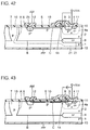
- Figs. 41 and 42 show in steps a state of a depletion layer in the high withstand voltage semiconductor device shown in Fig. 40 at the time of off-operation.
- electric potentials of drain electrode 12 and substrate electrode 13 are adapted to be 0V and a positive electric potential (+Vcc) is applied to gate electrode 9 and source electrode 11.
- This causes a depletion layer to widen mainly from a pn junction B which is an interface of n - layer 2 and p-type semiconductor substrate 1, a pn junction A which is an interface of n - layer 2 and p diffusion region 7, and a pn junction C which is an interface of n - layer 2 and p - diffusion region 5.
- a depletion layer extending from pn junction A normally widens more easily due to the influence of a depletion layer extending from pn junction B. Accordingly, the electric field in the vicinity of pn junction A is maintained to a relatively small value.
- This effect is realized by optimizing concentration of p-type semiconductor substrate 1, n-type impurity concentration contained in n - layer 2 and the thickness of n - layer 2, and is generally referred to as RESURF (REduced SURface Field) effect.
- a portion of the depletion layer extending from pn junction C widens towards n - layer 2 and at the same time makes p - diffusion region 5 depleted, since p - diffusion region 5 is a low concentration region.
- Gate electrode 9 and source electrode 11 formed overlapped above p - diffusion region 5 form a two-stage field plate. This promotes depletion of p - diffusion region 5 and relaxes an electric field of pn junction C in the vicinity of gate electrode 9.
- n + buried diffusion region 8 and p-type semiconductor substrate 1 have almost been depleted. Thus, the off-state can be maintained.
- Fig. 43 shows an on-state of the conventional high withstand voltage semiconductor device shown in Fig. 40.
- a potential of gate electrode 9 is lowered relative to that of source electrode 11. This inverts that surface of n - layer 2 directly under gate electrode 9 to p-type. This allows a hole current to flow from p + diffusion region 3 to p + diffusion region 6 via p - diffusion region 5 as shown by the arrows in Fig. 43.
- Most of the resistance of the device in the on-state comes from a resistance value of p - diffusion region 5.
- Fig. 44 is a partial cross sectional view of the second example of the conventional high withstand voltage semiconductor device. Referring to Fig. 44, it differs from the first example of the high withstand voltage semiconductor device shown in Fig. 40 in that an n + type diffusion 15 is formed within p + diffusion region 6. Other than that structure, the device is the same as the high withstand voltage semiconductor device shown in Fig. 40.
- Figs. 45-47 operation of the high withstand voltage semiconductor device shown in Fig. 44 will be described.
- Figs. 45 and 46 show in steps a state of depletion layer in the high withstand voltage semiconductor device shown in Fig. 44 at the time of off-operation. The description of the off-operation will not be repeated here since it is the same as the description in the case of the first example of the high withstand voltage semiconductor device shown in Fig. 40.
- Fig. 47 shows an on-state of the second example of the high withstand voltage semiconductor device.
- an electric potential of gate electrode 9 is decreased relative to that of source electrode 11. This allows the surface of n - layer 2 directly under gate electrode 9 to be inverted to p-type. This allows a hole current 37b to flow from p + diffusion region 3 to p + diffusion region 6 via p - diffusion region 5. Responsively, an electron current 37a from n + diffusion region 15 into both p - diffusion region 5 and n - layer 2. This implements a state in which many electrons and holes are stored and causes conductivity modulation. As a result, the on-state will be implemented. In other words, the second example of the high withstand voltage semiconductor device described above serves to operate as a p-channel IGBT.
- Fig. 48 is a bird's eye view of the entire structure of the second example of the high withstand voltage semiconductor device described above.
- FIG. 49 is a partial cross sectional view of the third example of the high withstand voltage semiconductor device.
- a buried oxide film 17 is formed on a surface of a semiconductor substrate 16.
- N - layer 2 is formed on buried oxide film 17.
- a trench 22 is formed at a predetermined position at n - layer 2.
- An oxide film 18 is formed on an inner surface of trench 22.
- a polysilicon layer 19 is buried inside oxide film 18.
- the high withstand voltage semiconductor device is similar to the first example of the high withstand voltage semiconductor device shown in Fig. 40.
- Figs. 50 and 51 show in steps a state of a depletion layer in the high withstand voltage semiconductor device at the time of off-operation.
- electric potentials of drain electrode 12 and substrate electrode 13 are set to be 0V and a positive electric potential (+V) is applied to gate electrode 9 and source electrode 11.
- This allows a depletion layer to extend mainly from a pn junction which is an interface of p - diffusion region 5 and n - layer 2 and from a pn junction which is an interface of p + diffusion region 6 and n - layer 2.
- the depletion layer starts to extend simultaneously from an interface of n - layer 2 and buried oxide film 17. This contributes to relaxation of electric field.
- the RESURF effect described above is obtained.
- the RESURF effect is described, for example, in S. Merchant et al. "Realization of High Breakdown Voltage (>700V) in Thin SOI Devices" Proc. of 3rd ISPSD, pp.31-35, 1991.
- on-operation of the third example of the high withstand voltage semiconductor device is shown in Fig. 52, its on-operation is not described here since it is the same as the on-operation of the first example of the high withstand voltage semiconductor device described above.
- FIG. 53 is a partial sectional view of the fourth example of the conventional high withstand voltage semiconductor device.
- n + diffusion region 3 and a p diffusion region 3a are formed in n - layer 2, and n + diffusion region 4 is formed at a surface of p + diffusion region 3. Furthermore, an n + diffusion region 15a is formed such that it is spaced apart from p + diffusion region 3. Furthermore, gate electrode 9 is formed on p diffusion region 3a positioned between n + diffusion region 4 and n - layer 2 with oxide film 10 interposed. Furthermore, source electrode 11 is formed in contact with surfaces of both p + diffusion region 3 and n + diffusion region 4. Drain electrode 12 is formed in contact with a surface of n + diffusion region 15a.
- Fig. 54 shows a state of a depletion layer of the fourth example of the high withstand voltage semiconductor device at the time of off-operation.
- electric potentials of source electrode 11, gate electrode 9 and substrate electrode 13 are adapted to be 0V, and a positive electric potential is applied to drain electrode 12.
- This allows a depletion layer to extend mainly from pn junction A which is an interface of p diffusion region 3a and n - layer 2.
- the depletion layer extends from an interface B of n - layer 2 and buried oxide film 17. This promotes expansion of the depletion layer, thus further widening the depletion layer. In other words, the RESURF effect is obtained. Consequently, a high withstand voltage device is obtained.
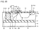
- Fig. 55 shows an on-state of the fourth example of the high withstand voltage semiconductor device.
- electric potentials of source electrode 11 and substrate electrode 13 are adapted to be 0V
- an electric potential of gate electrode 9 is increased relative to that of source electrode 11, and a positive electric potential (+Vcc) is applied to drain electrode 12.
- This allows a surface of p + diffusion region 3 directly under gate electrode 9 to be inverted to n-type, thereby forming an inverted region 38.
- This allows electrons from n + diffusion region 4 to reach n - layer 2 and n + diffusion region 15a via inverted region 38. Consequently, the on-operation will be implemented.
- the resistance value of p - diffusion region 5 is the factor which almost determines the resistance value of the high withstand voltage semiconductor device at the time of on-operation. Therefore, it is desired that the resistance of p - diffusion region 5 be decreased.
- the use of a technique which increases p-type impurity concentration contained in p - diffusion region 5 is generally considered. However, this restrains the widening of the depletion layer within p - diffusion region 5. Consequently, the electric field tends to be higher within the depletion layer and the withstand voltage of the high withstand voltage semiconductor device will be undesirably decreased.
- the resistance value of n - layer 2 serves as the factor which determines the resistance value of the high withstand voltage semiconductor device at the time of on-operation. Therefore, it is desired that the resistance of n - layer 2 be decreased.
- the use of a technique which increases n-type impurity concentration contained in n - layer 2 is considered.
- the widening of the depletion layer within n - layer 2 is restrained and the withstand voltage of the high withstand voltage semiconductor device will be degraded.
- the present invention is to solve the problems described above.
- the object of the invention is to provide a high withstand voltage semiconductor device capable of decreasing the resistance value of the device at the time of on-operation while hardly decreasing the withstand voltage of the device at the time of off-operation, and a method of manufacturing the same.
- the high withstand voltage semiconductor device includes a substrate having a main surface, a semiconductor layer of a first conductivity type, first and second impurity diffusion regions of a second conductivity type, a control electrode, and first and second main electrodes.
- the semiconductor layer is formed on the main surface of the substrate.
- the first and second impurity diffusion regions are formed such that they are spaced apart from each other on a surface of the semiconductor layer.
- the control electrode is formed on a surface of the semiconductor layer positioned between the first and second impurity diffusion regions with an insulating layer interposed.
- the first main electrode is electrically connected to the first impurity diffusion region.
- the second main electrode is electrically connected to the second impurity diffusion region.
- the second impurity diffusion region has a low concentration region containing impurity of the second conductivity type which has a relatively low concentration, and a plurality of high concentration regions containing impurity of the second conductivity type which has a relatively high concentration and connected to the low concentration region.
- the second impurity diffusion region includes both a low concentration region and a plurality of high concentration regions.
- a resistance value of the second impurity diffusion region can be decreased and a resistance value of the high withstand voltage semiconductor device at the time of on-operation can be decreased.
- a diffusion layer can be sufficiently widened in the low concentration region at the time of off-operation of the high withstand voltage semiconductor device. Accordingly, the widening of the depletion layer of the high withstand voltage semiconductor device at the time of off-operation will be promoted.
- the resistance value of the high withstand voltage semiconductor device at the time of on-operation can be decreased while hardly decreasing the withstand voltage of the high withstand voltage semiconductor device at the time of off-operation.
- the high withstand voltage semiconductor device is provided with a substrate having a main surface, a semiconductor layer of a first conductivity type, first, second and third impurity diffusion regions of a second conductivity type, a fourth impurity diffusion region of the first conductivity type, a control electrode, a first main electrode, and a second main electrode.
- the semiconductor layer is formed on the main surface of the substrate.
- the first impurity diffusion region is formed at a surface of the semiconductor layer.
- the second impurity diffusion region is formed on a surface of the semiconductor layer such that the second impurity diffusion region is spaced apart from the first impurity diffusion region.
- the control electrode is formed on a surface of the semiconductor layer positioned between the first and second impurity diffusion regions with an insulating layer interposed.
- the third impurity diffusion region is formed contiguous to that end of the second impurity diffusion region which is farther from the control electrode.
- the first main electrode is formed in contact with both a surface of the impurity diffusion region and a surface of the semiconductor layer positioned in the vicinity of the first impurity diffusion region.
- the fourth impurity diffusion region is formed at a surface of the third impurity diffusion region.
- the second main electrode is formed in contact with a surface of the fourth impurity diffusion region.
- a fifth impurity diffusion region of the first conductivity type containing impurity of the first conductivity type the amount of which is almost the same as that of the impurity of the first conductivity type contained in the semiconductor layer is formed, and the fifth impurity diffusion region is connected to the semiconductor layer.
- a fifth impurity diffusion region is formed at a surface of the second impurity diffusion region.
- the fifth impurity diffusion region and the semiconductor layer are positioned above and below the second impurity diffusion region, respectively.
- a depletion layer can extend from pn junctions positioned above and below the second impurity diffusion region. This allows the depletion layer to effectively extend within the second impurity diffusion region. Consequently, a high withstand voltage at the time of off-operation can be maintained.
- the high withstand voltage semiconductor device is provided with a substrate having a main surface, a semiconductor layer of a first conductivity type, a first impurity diffusion region of a second conductivity type, second and third impurity diffusion regions of the first conductivity type, a control electrode, and first and second main electrodes.
- the semiconductor layer is formed on the main surface of the substrate.
- the first impurity diffusion region is formed at a surface of the semiconductor layer.
- the second impurity diffusion region is formed at a surface of the first impurity diffusion region.
- the third impurity diffusion region is formed on a surface of the semiconductor layer such that the third impurity diffusion region is spaced apart from the first impurity diffusion region.
- the control electrode is formed on a surface of the first impurity diffusion region positioned between the second and third impurity diffusion regions with an insulating layer interposed.
- the first main electrode is formed in contact with both a surface of the second impurity diffusion region and a surface of the first impurity diffusion region proximate to the second impurity diffusion region.
- the second main electrode is formed in contact with a surface of the third impurity diffused region.
- a plurality of fourth impurity diffusion regions of the second type are formed at bottom regions of the semiconductor layer positioned between the first and third impurity diffusion regions.
- fourth impurity diffusion regions are formed at bottom regions of the semiconductor layer proximate to the main surface of the substrate.
- the widening of a depletion layer from a junction of the substrate in the semiconductor layer can be promoted.
- This improves a withstand voltage of the high withstand voltage semiconductor device at the time of off-operation.
- this maintains a high withstand voltage of the high withstand voltage semiconductor device, even when a concentration of the impurity of the first conductivity type contained in the semiconductor layer is increased. Consequently, a resistance value of the high withstand voltage semiconductor device at the time of on-operation can be decreased.
- the high withstand voltage semiconductor device in another aspect of the high withstand voltage semiconductor device according to the present invention, it is provided with a substrate having a main surface, a semiconductor layer of a first conductivity type, first and fourth impurity diffusion regions of a second conductivity type, second, third and fifth impurity diffusion regions of the first conductivity type, a control electrode, and first, second and third electrode layers.
- the semiconductor layer is formed on the main surface of the substrate.
- the first impurity diffusion region is formed at a surface of the semiconductor layer.
- the second and third impurity diffusion regions are formed such that they are spaced apart from each other on a surface of the first impurity diffusion region.
- the fourth impurity diffusion region is formed at a surface of the second impurity diffusion region.
- the fifth impurity diffusion region is formed on a surface of the first impurity diffusion region such that the fifth impurity diffusion region is spaced apart from the third impurity diffusion region.
- the control electrode is formed on a surface of the first impurity diffusion region positioned between the second and the third impurity diffusion regions with an insulating layer interposed.
- the first electrode layer is formed in contact with surfaces of the second and fourth impurity diffusion regions.
- the second electrode layer is formed in contact with a surface of the third impurity diffusion region.
- the third electrode layer is formed in contact with a surface of the fifth impurity diffusion region.
- the first impurity diffusion region positioned between the third and fifth impurity diffusion regions includes a low concentration region containing impurity of the second conductivity type which has a relatively low concentration, and a plurality of high concentration regions including impurity of the second conductivity type which has a relatively high concentration and spaced apart from one another.
- the first impurity diffusion region positioned between the third and fifth impurity diffusion regions has a low concentration region and high concentration regions.
- a depletion layer can be sufficiently widened in the low concentration region at the time of off-operation of the high withstand voltage semiconductor device. This improves the withstand voltage of the high withstand voltage semiconductor device at the time of off-operation.
- a resistance value of the first impurity diffusion region can be decreased. This decreases the resistance value of the high withstand voltage semiconductor device at the time of on-operation.
- the resistance value of the high withstand voltage semiconductor device at the time of on-operation can be decreased without decreasing the withstand voltage of the high withstand voltage semiconductor device at the time of off-operation.
- a semiconductor layer of a first conductivity type is firstly formed on a main surface of a substrate.
- An insulating layer is formed on a surface the semiconductor layer and the insulating layer is patterned.
- a conductive layer containing impurity of a second conductivity type having a relatively high concentration is formed such that it covers the patterned insulating layer and a surface of the semiconductor layer.
- the conductive layer is patterned, and the first impurity diffusion regions are electrically connected by the conductive layer. Furthermore, a second impurity diffusion region of the second conductivity type is formed on a surface of the semiconductor layer such that the second impurity diffusion region is spaced apart from the first impurity diffusion regions.
- a control electrode is formed on a surface of the semiconductor layer positioned between the first and the second impurity diffusion regions with an insulating layer interposed. First and second main electrodes are formed on portions of a surface of the semiconductor layer.
- a conductive layer containing the second conductivity type of impurity having a relatively high concentration is formed on a surface of the semiconductor layer, and a plurality of first impurity diffusion regions containing the second conductivity type of impurity having a relatively low concentration are formed by diffusing the impurity from the conductive layer into the semiconductor layer.
- the first impurity diffusion regions are connected to one another by the conductive layer.
- the conductive layer contains impurity of the second conductivity type having a relatively high concentration, its resistance value will be low.
- a resistance value of the current path can be decreased by providing the conductive layer described above. This decreases a resistance value of the high withstand voltage semiconductor device at the time of on-operation.
- a semiconductor layer of a first conductivity type is firstly formed on a main surface of a substrate.
- An insulating layer is formed on the main surface of the semiconductor layer and the insulating layer is patterned.
- a conductive layer containing impurity of the second conductivity type having a relatively high concentration is formed such that it covers surfaces of the insulating layer and the semiconductor layer.
- the conductive layer is patterned, and the first impurity diffusion regions are electrically connected by the conductive layer.
- a second impurity diffusion region of the second conductivity type is formed on a surface of the semiconductor layer such that the second impurity diffusion region is spaced apart from the first impurity diffusion region.
- a control electrode is formed on a surface of the semiconductor layer positioned between the first and second impurity diffusion regions with an insulating layer interposed. First and second main electrodes are formed on portions of a surface of the semiconductor layer.
- a plurality of the first impurity diffusion regions containing impurity of the second conductivity type having a relatively low concentration are connected by a conductive layer containing impurity having a relatively high concentration. This decreases a resistance value of the high withstand voltage semiconductor device at the time of on-operation, as is the case of the one aspect described above. Furthermore, by providing the first impurity diffusion regions, a high withstand voltage of the high withstand voltage semiconductor device at the time of off-operation can also be improved.
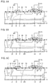
- Fig. 1 is a partial cross sectional view of a first embodiment of the high withstand voltage semiconductor device according to the present invention.
- Fig. 2 is a cross sectional view illustrating a state of a depletion layer of the high withstand voltage semiconductor device shown in Fig. 1 at the time of off-operation.
- Fig. 3A shows resistance components of the high withstand voltage semiconductor device shown in Fig. 1 at the time of on-operation.
- Fig. 3B shows resistance components of a conventional high withstand voltage semiconductor device at the time of on-operation.
- Fig. 4 shows the relation between surface concentration of a p - diffusion region and withstand voltage.
- Figs. 5A-5C show in steps a state of a depletion layer at the time of off-operation.
- concentration of p diffusion region 24 is uniformly increased.
- Figs. 6A-6C show in steps a state of a depletion layer of the high withstand voltage semiconductor device shown in Fig. 1 at the time of off-operation.
- Fig. 7 is a partial cross sectional view of a second embodiment of the high withstand voltage semiconductor device according to the present invention.
- Fig. 8 shows a state of a depletion layer of the high withstand voltage semiconductor device shown in Fig. 7 at the time of off-operation.
- Fig. 9 is a partial cross sectional view of a third embodiment of the high withstand voltage semiconductor device according to the present invention.
- Fig. 10 shows a state of a depletion layer of the high withstand voltage semiconductor device shown in Fig. 9 at the time of off-operation.
- Fig. 11 is a perspective view of a fourth embodiment of the high withstand voltage semiconductor device according to the present invention.
- Fig. 12 is a partial cross sectional view taken along the line XII-XII shown in Fig. 11.
- Fig. 13 shows a state of a depletion layer of the high withstand voltage semiconductor device shown in Fig. 11 at the time of off-operation.
- Fig. 14 is a partial cross sectional view of a fifth embodiment of the high withstand voltage semiconductor device according to the present invention.
- Fig. 15 shows a state of a depletion layer of the high withstand voltage semiconductor device shown in Fig. 14 at the time of off-operation.
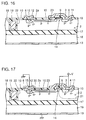
- Fig. 16 is a partial cross sectional view of a sixth embodiment of the high withstand voltage semiconductor device according to the present invention.
- Fig. 17 shows a state of a depletion layer of the high withstand voltage semiconductor device shown in Fig. 16 at the time of off-operation.
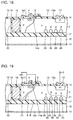
- Fig. 18 is a partial cross sectional view of a seventh embodiment of the high withstand voltage semiconductor device according to the present invention.
- Fig. 19 shows a state of a depletion layer of the high withstand voltage semiconductor device shown in Fig. 18 at the time of off-operation.
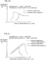
- Fig. 20 shows the relation between the specific resistance of n - layer and the withstand voltage of the high withstand voltage semiconductor device.
- Fig. 21 shows the relation between the thickness of the buried oxide film and the withstand voltage of the high withstand voltage semiconductor device.
- Fig. 22 is a partial cross sectional view of an eighth eighth embodiment of the high withstand voltage semiconductor device according to the present invention.
- Fig. 23 shows a state of a depletion layer of the high withstand voltage semiconductor device shown in Fig. 22 at the time of off-operation.
- Fig. 24 is a partial cross sectional view of a ninth embodiment of the high withstand voltage semiconductor device according to the present invention.
- Fig. 25 shows a state of a depletion layer of the high withstand voltage semiconductor device shown in Fig. 24 at the time of off-operation.
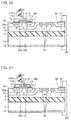
- Fig. 26 is a partial cross sectional view of a tenth embodiment of the high withstand voltage semiconductor device according to the present invention.
- Fig. 27 is a partial cross sectional view of a eleventh embodiment of the high withstand voltage semiconductor device according to the present invention.
- Fig. 28 is a cross sectional view of a first modification of the arrangement of p diffusion region 20 according to the present invention.
- Fig. 29 is a cross sectional view of a second modification of the arrangement of p diffusion region 20 according to the present invention.
- Fig. 30 is a cross sectional view of a third modification of the arrangement of p diffusion region 20 according to the present invention.
- Fig. 31 is a cross sectional view of a fourth modification of the arrangement of p diffusion region 20 according to the present invention.
- Fig. 32 is a cross sectional view of a fifth modification of the arrangement of p diffusion region 20 according to the present invention.
- Figs. 33-35 are cross sectional views illustrating the first to third steps of a first method of forming polysilicon layer 34a and p - diffusion region 5e shown in Fig. 32.
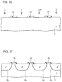
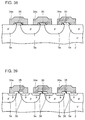
- Figs. 36-39 are cross sectional views illustrating the first to fourth steps of a second method of forming polysilicon layer 34a and p - diffusion region 5e shown in Fig. 32.
- Fig. 40 is a cross sectional view of a first example of a conventional high withstand voltage semiconductor device.
- Fig. 41 shows a state of a depletion layer of the conventional high withstand voltage semiconductor device shown in Fig. 40 at the time of off-operation.
- Fig. 42 shows a state of a depletion layer of the high withstand voltage semiconductor device shown in Fig. 40 at the time of off-operation.
- Fig. 43 shows an on-operation of the high withstand voltage semiconductor device shown in Fig. 40.
- Fig. 44 is a partial cross sectional view of a second example of the conventional high withstand voltage semiconductor device.
- Fig. 45 shows a state of a depletion layer of the conventional high withstand voltage semiconductor device shown in Fig. 44 at the time of off-operation.
- Fig. 46 shows a state of a depletion layer of the high withstand voltage semiconductor device shown in Fig. 44 at the time of off-operation.
- Fig. 47 shows an on-operation of the high withstand voltage semiconductor device shown in Fig. 44.
- Fig. 48 is a bird's eye view of the entire structure of the high withstand voltage semiconductor device shown in Fig. 44.
- Fig. 49 is a partial cross sectional view of a third example of the conventional high withstand voltage semiconductor device.
- Fig. 50 shows a state of a depletion layer of the conventional high withstand voltage semiconductor device shown in Fig. 49 at the time of off-operation.
- Fig. 51 shows a state of the depletion layer of the high withstand voltage semiconductor device shown in Fig. 49 at the time of off-operation.
- Fig. 52 shows an on-operation of the high withstand voltage semiconductor device shown in Fig. 49.
- Fig. 53 is a partial cross sectional view of a fourth example of the conventional high withstand voltage semiconductor device.
- Fig. 54 shows a state of a depletion layer of the conventional high withstand voltage semiconductor device shown in Fig. 53 at the time of off-operation.
- Fig. 55 shows an off-operation of the high withstand voltage semiconductor device shown in Fig. 53.
- Fig. 1 is a partial cross sectional view of a first embodiment of the present invention. More specifically, the figure shows an embodiment in which the present invention is applied to a p-channel MOS device.
- an n - layer 2 is formed on a main surface of p-type semiconductor substrate 1.
- a p diffusion region 7 is formed such that it penetrates n - layer 2 to reach p-type semiconductor substrate 1.
- a p-channel MOS transistor 14 is formed at a surface of n - layer 2.
- P-channel MOS transistor 14 is provided with a p - diffusion region 5, a p + diffusion region 3 and a gate electrode 9.
- Gate electrode 9 is formed on a surface of n - layer 2 positioned between p - diffusion region 5 and p + diffusion region 3 with an oxide film 10 interposed.
- n + diffusion region 4 is formed adjacent to p + diffusion region 3. Furthermore, a p + diffusion region 6 is formed contiguous to one end of p - diffusion region 5.
- a drain electrode 12 is formed in contact with a surface of p + diffusion region 6, and a source electrode 11 is formed in contact with a surface of p + diffusion region 3 and a surface of n + diffusion region 4. Source electrode 11 extends above gate electrode 9 and on p - diffusion region 5, as shown in Fig. 1.
- a p diffusion region 20 is formed such that it reaches n - layer 2 from p + diffusion region 5.
- p diffusion region 20 has a ring-shaped planar structure.
- p diffusion region 20 will be described in detail. It is preferred that a p-type impurity concentration contained in p diffusion region 20 (in the present specification, "impurity concentration” means the peak concentration of the impurity) be at least approximately 10-100 times p-type impurity concentration contained in p - diffusion region 5. Furthermore, it is preferred that a plurality of p diffusion regions 20 be provided such that they are spaced apart from one another in the longitudinal direction of p - diffusion region 5. By providing a plurality of p diffusion regions 20 such that they are spaced apart from one another in p - diffusion region 5 as described, the widening of a depletion layer of the high withstand voltage semiconductor device at the time of off-operation will be promoted in the horizontal direction.
- Fig. 2 shows a state of a depletion layer of the first embodiment of the high withstand voltage semiconductor device at the time of off-operation.
- the reference numeral 21 indicates an edge of the depletion layer.
- electric potentials of a substrate electrode 13 and drain electrode 12 are set to be 0V, and a positive electric potential (+V) is applied to gate electrode 9 and source electrode 11. This allows a depletion layer to widen from pn junctions A, B and C.
- the widening of the depletion layer in the horizontal direction is promoted in the vicinity of a surface of n - layer 2 due to the presence of ring-shaped p diffusion region 20.
- a non-depleted region 30 remains at portions of p + diffusion region 6 and p diffusion region 20, the depletion layer is sufficiently widened in n - layer 2. This relaxes an electric field strength in the depletion layer and the same effect as the RESURF effect is obtained.
- the structure corresponding to ring-shaped p diffusion region 20 is referred to as Floating Field Rings and has an effect to promote widening of a depletion layer. This is described, for example, in B.J. Balign, Modern Power Devices , 1987, pp.92-99.
- FIG. 3A shows a state of the on-operation of the high withstand voltage semiconductor device shown in Fig. 1.
- Fig. 3B shows a state of a conventional high withstand voltage semiconductor device at the time of on-operation.
- the on-operation of the high withstand voltage semiconductor device is implemented by adapting electric potentials of drain electrode 12 and substrate electrode (not shown) to be 0V, applying a positive electric potential (+Vcc) to source electrode 11 and decreasing an electric potential of gate electrode 9 as compared with that of source electrode 11. Then, a surface of n - layer 2 directly under gate electrode 9 is inverted to p-type and a current flows from source electrode 11 to drain electrode 12.
- the resistance components of p - diffusion region 5 are indicated as R A1 , R A2 ... R Am
- the resistance components of p diffusion region 20 are indicated as R B1 , R B2 ... R Bn
- the resistance component of a channel region directly under gate electrode 9 is indicated as Rch.
- the resistance components of p - diffusion region 5 the position of which corresponds to that of p diffusion region 20 of the conventional example are indicated as R C1 , R C2 ... R Cn .
- each of the total resistances is expressed as follows:
- Fig. 4 shows a result of computer simulation regarding the change in withstand voltage of the high withstand voltage semiconductor device relative to the surface concentration of p - diffusion region 5.
- Conditions corresponding to p-type semiconductor substrate 1 are controlled and two models have been examined which have withstand voltages of 450V and 600V, respectively, in the absence of p - diffusion region 5.
- the withstand voltage of either of the two models tends to decrease as surface concentration increases.
- the withstand voltage of either of the two models decreases to approximately 150V regardless of the initial design conditions.
- Figs. 5A-5C are cross sectional views illustrating a state of a depletion layer when positive electric potentials (+V1 ⁇ +V2 ⁇ +V3) are sequentially applied to a high withstand voltage semiconductor device having a p diffusion region 24 the concentration of which is uniformly increased.
- Fig. 6A-6C are cross sectional views illustrating a state of a depletion layer when the positive electric potentials +V1, +V2, +V3 described above are sequentially applied to the first embodiment of the high withstand voltage semiconductor device.
- a depletion layer starts to extend from pn junctions A, B, C. Then, by applying a higher electric potential, the depletion layer extends towards source electrode 11 as shown in Figs. 5B and 5C.
- the concentration of p diffusion region 24 is uniformly high, the degree of the widening of the depletion layer gradually decreases as it approaches source electrode 11. Then, as shown in Fig. 5C, there is generated an electric field concentration point 32, causing an avalanche breakdown.
- the depletion layer extends smoothly towards source electrode 11 as higher voltages are sequentially applied.
- p - diffusion region 5 exists between p diffusion regions 20.
- a non-depleted region 30 remains in diffusion region 20 when the depletion layer extends.
- the widening of the depletion layer is promoted.
- depletion layer continues to extend while p - diffusion region 5 is completely depleted.
- the depletion layer expands sufficiently and a withstand voltage of the high withstand voltage semiconductor device can be improved at the time of off-operation.
- the resistance value of the high withstand voltage semiconductor device at the time of on-operation can be decreased without degrading the withstand voltage of the high withstand voltage semiconductor device at the time of off-operation.
- FIG. 7 is a partial cross sectional view of the second embodiment of the high withstand voltage semiconductor device of the present invention.
- the high withstand voltage semiconductor device shown in the figure differs from the one shown in Fig. 1 in that an n + buried diffusion region 8 is formed. Other than that structure, the device is the same as the one shown in Fig. 1.
- Fig. 8 shows a state of a depletion layer of the high withstand voltage semiconductor device shown in Fig. 7 at the time of off-operation.
- the depletion layer can be prevented from widening in n - layer 2 positioned between n + buried diffusion region 8 and p + diffusion region 3, as shown in Fig. 8. Accordingly, the depletion layer extends in p-type semiconductor substrate 1 positioned under n + buried diffusion region 8. At that time, the depletion layer can be sufficiently widened, since p-type semiconductor substrate 1 has a low concentration and is thick. This further improves a withstand voltage of the high withstand voltage semiconductor device at the time of off-operation.
- FIG. 9 is a partial sectional view of the third embodiment of the high withstand voltage semiconductor device according to the present invention.
- a buried oxide film 17 is formed on a surface of a semiconductor substrate 16 and n - layer 2 is formed on a surface of buried oxide film 17.
- a high withstand voltage semiconductor device having the SOI (Semiconductor On Insulator) structure is shown.
- a trench 22 is provided so that it penetrates n - layer 2, and an oxide film 18 and a polysilicon layer 18 are buried within trench 22.
- the device is the same as the first embodiment of the high withstand voltage semiconductor device shown in Fig. 1.
- Fig. 10 shows a state of a depletion layer of the third embodiment of the high withstand voltage semiconductor device at the time of off-operation.
- the depletion layer extends sufficiently in n - layer 2 while a non-depleted region 30 remains.
- the expansion of the depletion layer is promoted in the horizontal direction due to the presence of p diffusion region 20 and p - diffusion region 5. This allows the RESURF effect to occur effectively, and the withstand voltage at the time of off-operation is improved.
- the same effect as the case of the first embodiment can be obtained.
- FIG. 11 is a partial cross sectional, perspective view of the fourth embodiment of the high withstand voltage semiconductor device according to the present invention.
- a p diffusion region 23 containing p-type impurity the concentration of which is higher than that of p-type impurity contained in p - diffusion region 5 is formed, and an n - diffusion region 2a is provide at a surface of p diffusion region 23. Furthermore, an n + diffusion region 15 is formed on a surface of p + diffusion region 6. Other than that structure, the device is almost the same as the high withstand voltage semiconductor device shown in Fig. 1.
- n - diffusion region 2a provided on a surface of p diffusion region 23 as described above, a region in which modulation occurs by electron implantation is formed above and below p diffusion region 23 at the time of on-operation. This improves modulation efficiency and accelerates switching operation rate.
- Fig. 12 shows a part of the cross section taken along the line XII-XII shown in Fig. 11.
- p diffusion region 23 has a gap 31 at its side. Gap 31 allows formation of a region in which modulation occurs at the right and left sides of p diffusion region 23, as well as above and below p diffusion region 23. This further improves modulation efficiency.
- the gap 31 described above connects n - diffusion region 2a with n - layer 2.
- FIG. 13 shows a state of a depletion layer of the fourth embodiment of the high withstand voltage semiconductor device at the time of off-operation.
- a predetermined voltage is applied under the same voltage applying conditions as is in the first embodiment described above. This allows expansion of a depletion layer from pn junctions A, B, C, D. Particularly, a portion of the depletion layer extending from pn junctions C, D grows such that it sandwiches p diffusion region 23 between upper and lower portions, as indicated by arrows 25 in Fig. 13. This promotes the depletion of p diffusion region 23, and the RESURF effect can be obtained effectively. This improves a withstand voltage of the high withstand voltage semiconductor device at the time of off-operation.
- p diffusion region 23 since the depletion of p diffusion region 23 is further promoted as described above, a p-type impurity concentration of p diffusion region 23 can be increased more than that of p - diffusion region 5. This decreases a resistance value of the high withstand voltage semiconductor device at the time of on-operation.
- FIG. 14 is a partial cross sectional view of the fifth embodiment of the high withstand voltage semiconductor device according to the present invention. More specifically, the figure shows an embodiment in which the present invention is applied to the IGBT.
- the fifth embodiment of the high withstand voltage semiconductor device differs from the high withstand voltage semiconductor device shown in Fig. 1 in that n + buried diffusion region 8 is formed.
- n + buried diffusion region 8 By providing n + buried diffusion region 8, it becomes possible to expand a depletion layer in p-type semiconductor substrate 1 positioned under n + buried diffusion region 8 at the time of off-operation, as shown in Fig. 15. This further improves a withstand voltage of the high withstand voltage semiconductor device, as is in the second embodiment described above.
- FIG. 16 is a partial cross sectional view of the sixth embodiment of the high withstand voltage semiconductor device according to the present invention.
- n - layer 2 is formed on a surface of p-type semiconductor substrate 16 with buried oxide film 17 interposed.
- Trench 22 is provided such that it penetrates n - layer 2, and oxide film 18 and polysilicon layer 19 are buried in trench 22.
- the device is the same as the high withstand voltage semiconductor device shown in Fig. 11.
- FIG. 18 is a cross sectional view of the seventh embodiment of the high withstand voltage semiconductor device according to the present invention. More specifically, the figure shows an embodiment in which the present invention is applied to n-channel MOS device.
- buried oxide film 17 is formed on a surface of semiconductor substrate 16.
- N - layer 2 is formed on buried oxide film 17.
- An n-channel MOS transistor 14a is formed at a surface of n - layer 2.
- N-channel MOS transistor 14a consists of n + diffusion region 4, gate electrode 9 and n - layer 2. Furthermore, a p diffusion region 3a is formed in n - layer 2.
- n + diffusion region 15a is formed such that it is spaced apart from p diffusion region 3a.
- Drain electrode 12 is formed in contact with a surface of n + diffusion region 15a, and source electrode 11 is formed in contact with a surface of p diffusion region 3a and a surface of n + diffusion region 4.
- Trench 22 is formed such that it penetrates n - layer 2 to reach buried oxide film 17, and oxide film 18 and polysilicon layer 19 are buried in trench 22. Furthermore, a p diffusion region 26 is formed at a bottom region of n - layer 2 positioned between p diffusion region 3a and n + diffusion region 15a such that p diffusion region 26 is adjacent to buried oxide film 17.
- a plurality of p diffusion regions 26 may be provided such that they are spaced apart from one another, as shown in Fig. 18, or the adjacent p diffusion regions 26 may be connected to each other by, for example, a p-type low concentration region.
- a p-type impurity concentration contained in p diffusion region 26 may be the same as or more than a p-type impurity concentration contained in diffusion region 3a.
- the p-type impurity concentration contained in p diffusion region 26 is approximately 10-100 times the p-type impurity concentration contained in p diffusion region 3a.
- Fig. 19 shows a state of a depletion layer in the seventh embodiment of the high withstand voltage semiconductor device at the time of off-operation.
- electric potentials of source electrode 11, gate electrode 9 and substrate electrode 13 are set to be 0V and a positive electric potential (+V) is applied to drain electrode 12. This allows a depletion layer to extend from pn junction A and an interface E.
- p diffusion region 26 As shown in Fig. 19, by providing p diffusion region 26 at the bottom of n - layer 2 positioned between p diffusion region 3a and n + diffusion region 15a, p diffusion region 26 will have a function to promote the widening of the depletion layer in the horizontal direction. Furthermore, by providing a plurality of p diffusion regions 26 towards the bottom region of n - layer 2 positioned directly under drain electrode 12, the function to promote the widening of the depletion layer in the horizontal direction will further be improved.
- the widening of the depletion layer is promoted in the horizontal direction and the RESURF effect is obtained effectively.
- a withstand voltage of the high withstand voltage semiconductor device at the time of off-operation can be improved.
- p diffusion region 26 it becomes possible to widen the range of the value of various parameters related to the determination of withstand voltage in which a certain constant withstand voltage is maintained.
- Fig. 20 shows change in withstand voltage of the high withstand voltage semiconductor devices relative to the specific resistance of n - layer 2.
- the characteristic of a conventional example is indicated with the solid line.
- Fig. 20 shows a tendency that the withstand voltage slightly increases with decreased specific resistance of n - layer 2 and then the withstand voltage rapidly decreases.
- Fig. 21 shows change in withstand voltage of the high withstand voltage semiconductor device relative to the thickness of the buried oxide film.
- the solid line indicates the characteristic of a conventional example.
- the withstand voltage increases with increased thickness of the buried oxide film, the withstand voltage rapidly decreases when the thickness of the buried oxide film reaches a certain value. This tendency is attributed to a constraint on the widening of the depletion layer expanding from interface E into n - layer 2 in Fig. 19.
- the characteristic changes to the one indicated with the dotted line in Fig. 21 when forming p diffusion region 26 is performed.
- a high withstand voltage can be maintained. Accordingly, it becomes possible to design devices with sufficient margins in thickness and specific resistance of n - layer 2, and a device can be easily manufactured which takes into consideration the decrease in the device resistance and rapid switching.
- FIG. 22 is a partial cross sectional view of the eighth embodiment of the high withstand voltage semiconductor device according to the present invention.
- the device differs from the high withstand voltage semiconductor device shown in Fig. 18 in that an n diffusion region 23a is formed at a bottom region of n - layer 2 positioned directly under n + diffusion region 15a.
- the device is the same as the high withstand voltage semiconductor device shown in Fig. 18.
- Fig. 23 shows a state of a depletion layer in the high withstand voltage semiconductor device shown in Fig. 22 at the time of off-operation.
- off-state is implemented under the same conditions as in the case of the seventh embodiment described above.
- a depletion layer starts to extend from pn junction A and interface E. Then, the widening of the depletion layer is promoted in the horizontal direction due to the presence of p diffusion region 26. Accordingly, the RESURF effect is obtained effectively.
- FIG. 24 is a partial cross sectional view of the ninth embodiment of the high withstand voltage semiconductor device of the present invention.
- p diffusion region 26 is formed such that it is spaced apart from an interface of buried oxide film 17 and n - layer 2.
- the device is the same as the high withstand voltage semiconductor device shown in Fig. 18.
- Fig. 25 shows a state of a depletion layer in the ninth embodiment of the high withstand voltage semiconductor device shown in Fig. 24 at the time of off-operation. As shown in Fig. 25, the depletion layer can be sufficiently widened in the horizontal direction and the RESURF effect can be obtained effectively.
- FIG. 26 is a partial cross sectional view of the tenth embodiment of the high withstand voltage semiconductor device according to the present invention. More specifically, the figure shows an embodiment in which the concept of the present invention is applied to a p-channel EST.
- n - layer 2 is formed on a surface of semiconductor substrate 16 with buried oxide film 17 interposed.
- a p - diffusion region 27 is formed on a surface of n - layer 2.
- N diffusion regions 28a, 28b and on n + diffusion region 39 are provided such that they are spaced apart from each another at a surface of p - diffusion region 27.
- An n + diffusion region 40 and a p + diffusion region 29a are formed on a surface of n diffusion region 28a.
- a source electrode 11a is formed in contact with both n + diffusion region 40 and p + diffusion region 29a, and a source electrode 11b is formed in contact with a p + diffusion region 29b. Furthermore, gate electrode 9 is formed on a surface of p - diffusion region 27 positioned between n diffusion region 28a and n diffusion region 28b with oxide film 10 interposed. Furthermore, drain electrode 12 is formed in contact with a surface of n + diffusion region 39.
- a p diffusion region 33 is provided at p - diffusion region 27 positioned between n diffusion region 28b and n + diffusion region 39.
- a p-type impurity concentration contained in p diffusion region 33 is more than approximately 10-100 times p-type impurity concentration contained in p - diffusion region 27.
- a plurality of p diffusion regions 33 be provided such that they are spaced apart from one another.
- the widening of the depletion layer in the horizontal direction at the time of off-operation can be effectively promoted. Furthermore, as the concentration of p diffusion region 33 is relatively higher than that of p - diffusion region 27, a resistance of a current path at the time of on-operation can also be decreased. This decreases the device resistance.
- FIG. 11 is a cross sectional view of the eleventh embodiment of the high withstand voltage semiconductor device according to the present invention.
- the eleventh embodiment of the high withstand voltage semiconductor device differs from the tenth embodiment of the high withstand voltage semiconductor device shown in Fig. 26 in that an n + diffusion region 41 is formed in place of p + diffusion region 29b.
- the device is the same as the tenth embodiment of the high withstand voltage semiconductor device described above.
- the eleventh embodiment illustrates a high withstand voltage semiconductor device in which the concept of the present invention is applied to a p-channel BRT.
- the same effect as the case of the tenth embodiment described above will be obtained.
- Fig. 28 is a partially enlarged cross sectional view of the first modification of p diffusion region 20.
- a p diffusion region 20a and a p - diffusion region 5a are arranged alternately, a diffusion depth of each being almost the same. In this structure also, almost the same effect as the case shown in Fig. 1 is obtained.
- Fig. 29 is a partially enlarged cross sectional view of the second modification of p diffusion region 20.
- the diffusion depth of a p diffusion region 20b is made shallower than the diffusion depth of a p - diffusion region 5b. This further promotes the widening of the depletion layer in the horizontal direction when compared with the case shown in Fig. 1.
- FIG. 30 is a partially enlarged cross sectional view of the third modification of p diffusion region 20.
- a polysilicon layer 34 introducing a high concentration p-type impurity may be formed on a surface of n - layer 2.
- a plurality of p - layers 5c are formed on a surface of n - layer 2 such that they are spaced apart from one another, the adjacent p - diffusion regions 5c being electrically connected by polysilicon layer 34.
- the concentration of polysilicon layer 34 can be rendered extremely high, further decreasing device resistance at the time of on-operation when compared with the case of the first embodiment shown in Fig. 1.
- FIG. 31 is a partially enlarged cross sectional view of the fourth modification of p diffusion region 20.
- a plurality of p diffusion regions 20c are provided on the surface of a p - diffusion region 5d such that they are spaced apart from one another.
- this structure also, the same effect as the case of the first embodiment shown in Fig. 1 will be obtained.
- FIG. 32 is a partially enlarged cross sectional view of the fifth modification of p diffusion region 20.
- a polysilicon layer 34a is formed on a surface of n - layer 2 with an insulating layer 35 interposed. Furthermore, a p + diffusion region 36 is formed such that it surrounds a contact portion of polysilicon layer 34a and a p - diffusion region 5e.
- the present modification is the same as the third modification described above. In the present modification also, almost the same effect as the case of the third modification described above is obtained.
- insulating layer 35 of silicon oxide film is deposited on a surface of n - layer 2 using the CVD method. Then, after insulating layer 35 is patterned to a predetermined pattern, polysilicon layer 34a introducing a high concentration p-type impurity is formed using the CVD method, for example, such that it covers insulating layer 35 and a surface of n - layer 2.
- p - diffusion regions 5e are formed such that they are spaced apart from one another.
- polysilicon layer 34a is patterned to a predetermined pattern. Through the process described above, polysilicon layer 34a and p - diffusion region 5e shown in Fig. 32 are formed.
- a second method of manufacturing polysilicon layer 34a and p - diffusion region 5e will be described.
- a p-type impurity such as boron ion (B + ) is selectively implanted at a surface of n - layer 2 by using insulating layer 35 as a mask.
- p - diffusion regions 5e are formed such that they are spaced apart from one another, as shown in Fig. 37.
- polysilicon layer 34a is formed through the same process as shown in the case of the first manufacturing method described above. Then, by heat treatment of polysilicon layer 34a, p + diffusion region 36 is formed on a surface of p - diffusion region 5e, as shown in Fig. 39. Through the process described above, polysilicon layer 34a and p - diffusion region 5e shown in Fig. 32 are formed. Then, gate electrode 9, p + diffusion region 3, 6, oxide film 10, source electrode 11, drain electrode 12 etc. are formed.
- the first to fifth modifications described above can be applied not only to the first embodiment but also to all of the other p-channel devices.
Landscapes
- Insulated Gate Type Field-Effect Transistor (AREA)
- Thin Film Transistor (AREA)
- Thyristors (AREA)
Priority Applications (2)
| Application Number | Priority Date | Filing Date | Title |
|---|---|---|---|
| EP07018406A EP1868234A3 (de) | 1995-08-22 | 1996-03-26 | Hochspannungsbeständige Halbleitervorrichtung und Herstellungsverfahren dafür |
| EP10182259A EP2261990A3 (de) | 1995-08-22 | 1996-03-26 | Hochspannungsbeständige Halbleitervorrichtung und Herstellungsverfahren dafür |
Applications Claiming Priority (2)
| Application Number | Priority Date | Filing Date | Title |
|---|---|---|---|
| JP213523/95 | 1995-08-22 | ||
| JP21352395A JP3581447B2 (ja) | 1995-08-22 | 1995-08-22 | 高耐圧半導体装置 |
Related Child Applications (3)
| Application Number | Title | Priority Date | Filing Date |
|---|---|---|---|
| EP07018406A Division EP1868234A3 (de) | 1995-08-22 | 1996-03-26 | Hochspannungsbeständige Halbleitervorrichtung und Herstellungsverfahren dafür |
| EP07018406.4 Division-Into | 2007-09-19 | ||
| EP10182259.1 Division-Into | 2010-09-29 |
Publications (3)
| Publication Number | Publication Date |
|---|---|
| EP0759638A2 true EP0759638A2 (de) | 1997-02-26 |
| EP0759638A3 EP0759638A3 (de) | 1999-05-06 |
| EP0759638B1 EP0759638B1 (de) | 2011-07-13 |
Family
ID=16640608
Family Applications (3)
| Application Number | Title | Priority Date | Filing Date |
|---|---|---|---|
| EP96104778A Expired - Lifetime EP0759638B1 (de) | 1995-08-22 | 1996-03-26 | Halbleiterbauelement mit hoher Spannungsfestigkeit und dessen Herstellungsverfahren |
| EP10182259A Withdrawn EP2261990A3 (de) | 1995-08-22 | 1996-03-26 | Hochspannungsbeständige Halbleitervorrichtung und Herstellungsverfahren dafür |
| EP07018406A Withdrawn EP1868234A3 (de) | 1995-08-22 | 1996-03-26 | Hochspannungsbeständige Halbleitervorrichtung und Herstellungsverfahren dafür |
Family Applications After (2)
| Application Number | Title | Priority Date | Filing Date |
|---|---|---|---|
| EP10182259A Withdrawn EP2261990A3 (de) | 1995-08-22 | 1996-03-26 | Hochspannungsbeständige Halbleitervorrichtung und Herstellungsverfahren dafür |
| EP07018406A Withdrawn EP1868234A3 (de) | 1995-08-22 | 1996-03-26 | Hochspannungsbeständige Halbleitervorrichtung und Herstellungsverfahren dafür |
Country Status (3)
| Country | Link |
|---|---|
| US (2) | US5804864A (de) |
| EP (3) | EP0759638B1 (de) |
| JP (1) | JP3581447B2 (de) |
Cited By (2)
| Publication number | Priority date | Publication date | Assignee | Title |
|---|---|---|---|---|
| EP1138082A1 (de) * | 1999-09-16 | 2001-10-04 | Koninklijke Philips Electronics N.V. | Halbleiterbauelement |
| WO2004053995A3 (de) * | 2002-12-10 | 2004-09-16 | Infineon Technologies Ag | Halbleiterschaltungsanordnung |
Families Citing this family (31)
| Publication number | Priority date | Publication date | Assignee | Title |
|---|---|---|---|---|
| JP3918209B2 (ja) * | 1996-09-11 | 2007-05-23 | 株式会社デンソー | 絶縁ゲート型バイポーラトランジスタ及びその製造方法 |
| JPH10321842A (ja) * | 1997-05-15 | 1998-12-04 | Toshiba Microelectron Corp | 半導体装置 |
| JP3850146B2 (ja) | 1998-07-07 | 2006-11-29 | 三菱電機株式会社 | 分離構造とその分離構造を備える半導体装置 |
| JP2001102569A (ja) * | 1999-09-28 | 2001-04-13 | Fuji Electric Co Ltd | 半導体デバイス |
| ATE514192T1 (de) * | 2000-03-31 | 2011-07-15 | Ihp Gmbh | Cmos-kompatibler lateraler dmos-transistor |
| JP4977927B2 (ja) * | 2000-10-23 | 2012-07-18 | 日本電気株式会社 | 薄膜トランジスタ及びそれを用いた液晶表示装置 |
| US6936908B2 (en) * | 2001-05-03 | 2005-08-30 | Ixys Corporation | Forward and reverse blocking devices |
| US8093652B2 (en) * | 2002-08-28 | 2012-01-10 | Ixys Corporation | Breakdown voltage for power devices |
| CN100483733C (zh) * | 2003-01-15 | 2009-04-29 | 克里公司 | 碳化硅器件的边缘环形端接 |
| US7026650B2 (en) * | 2003-01-15 | 2006-04-11 | Cree, Inc. | Multiple floating guard ring edge termination for silicon carbide devices |
| US9515135B2 (en) | 2003-01-15 | 2016-12-06 | Cree, Inc. | Edge termination structures for silicon carbide devices |
| US8901699B2 (en) | 2005-05-11 | 2014-12-02 | Cree, Inc. | Silicon carbide junction barrier Schottky diodes with suppressed minority carrier injection |
| EP1722423B1 (de) * | 2005-05-12 | 2016-07-06 | Ixys Corporation | Stabile Dioden für Niedrig- und Hochfrequenzanwendungen |
| US7541660B2 (en) * | 2006-04-20 | 2009-06-02 | Infineon Technologies Austria Ag | Power semiconductor device |
| JP2008004649A (ja) * | 2006-06-21 | 2008-01-10 | Matsushita Electric Ind Co Ltd | 半導体装置及びその製造方法 |
| JP2008124421A (ja) * | 2006-10-17 | 2008-05-29 | Matsushita Electric Ind Co Ltd | 半導体装置及びその製造方法 |
| US20100171175A1 (en) * | 2009-01-05 | 2010-07-08 | Fan bing-yao | Structure For High Voltage/High Current MOS Circuits |
| JP5543758B2 (ja) | 2009-11-19 | 2014-07-09 | ルネサスエレクトロニクス株式会社 | 半導体装置 |
| JP5663275B2 (ja) * | 2010-11-10 | 2015-02-04 | 新電元工業株式会社 | 半導体装置の製造方法 |
| JP5719167B2 (ja) | 2010-12-28 | 2015-05-13 | ルネサスエレクトロニクス株式会社 | 半導体装置 |
| CN103165460B (zh) * | 2011-12-16 | 2016-05-04 | 中芯国际集成电路制造(上海)有限公司 | Ldnmos及ldpmos的制造方法 |
| WO2013136550A1 (ja) * | 2012-03-16 | 2013-09-19 | 三菱電機株式会社 | 半導体装置およびその製造方法 |
| US9231083B2 (en) * | 2012-06-29 | 2016-01-05 | Freescal Semiconductor Inc. | High breakdown voltage LDMOS device |
| US9599590B2 (en) | 2012-10-12 | 2017-03-21 | Sage Science, Inc. | Side-eluting molecular fractionator |
| JP6192952B2 (ja) * | 2013-03-04 | 2017-09-06 | ラピスセミコンダクタ株式会社 | 半導体装置の製造方法 |
| DE102014005879B4 (de) * | 2014-04-16 | 2021-12-16 | Infineon Technologies Ag | Vertikale Halbleitervorrichtung |
| JP5872621B2 (ja) * | 2014-05-09 | 2016-03-01 | ルネサスエレクトロニクス株式会社 | 半導体装置 |
| US10131901B2 (en) | 2014-10-15 | 2018-11-20 | Sage Science, Inc. | Apparatuses, methods and systems for automated processing of nucleic acids and electrophoretic sample preparation |
| US11542495B2 (en) | 2015-11-20 | 2023-01-03 | Sage Science, Inc. | Preparative electrophoretic method for targeted purification of genomic DNA fragments |
| CN110506203A (zh) | 2017-04-07 | 2019-11-26 | 塞奇科学股份有限公司 | 用于通过使用集成电泳dna纯化来检测遗传结构变异的系统和方法 |
| JP7102934B2 (ja) * | 2018-05-22 | 2022-07-20 | 株式会社デンソー | 半導体装置 |
Family Cites Families (20)
| Publication number | Priority date | Publication date | Assignee | Title |
|---|---|---|---|---|
| US4300150A (en) * | 1980-06-16 | 1981-11-10 | North American Philips Corporation | Lateral double-diffused MOS transistor device |
| GB2134705B (en) * | 1983-01-28 | 1985-12-24 | Philips Electronic Associated | Semiconductor devices |
| GB2173037A (en) * | 1985-03-29 | 1986-10-01 | Philips Electronic Associated | Semiconductor devices employing conductivity modulation |
| US4989058A (en) * | 1985-11-27 | 1991-01-29 | North American Philips Corp. | Fast switching lateral insulated gate transistors |
| US5241210A (en) * | 1987-02-26 | 1993-08-31 | Kabushiki Kaisha Toshiba | High breakdown voltage semiconductor device |
| US5105243A (en) * | 1987-02-26 | 1992-04-14 | Kabushiki Kaisha Toshiba | Conductivity-modulation metal oxide field effect transistor with single gate structure |
| EP0360036B1 (de) * | 1988-09-20 | 1994-06-01 | Siemens Aktiengesellschaft | Planarer pn-Übergang hoher Spannungsfestigkeit |
| US5132753A (en) * | 1990-03-23 | 1992-07-21 | Siliconix Incorporated | Optimization of BV and RDS-on by graded doping in LDD and other high voltage ICs |
| IT1247293B (it) * | 1990-05-09 | 1994-12-12 | Int Rectifier Corp | Dispositivo transistore di potenza presentante una regione ultra-profonda, a maggior concentrazione |
| JP2650519B2 (ja) * | 1991-07-25 | 1997-09-03 | 株式会社日立製作所 | 横型絶縁ゲートトランジスタ |
| US5319222A (en) * | 1992-04-29 | 1994-06-07 | North Carolina State University | MOS gated thyristor having on-state current saturation capability |
| TW218424B (de) * | 1992-05-21 | 1994-01-01 | Philips Nv | |
| JP3076468B2 (ja) * | 1993-01-26 | 2000-08-14 | 松下電子工業株式会社 | 半導体装置 |
| US5313082A (en) * | 1993-02-16 | 1994-05-17 | Power Integrations, Inc. | High voltage MOS transistor with a low on-resistance |
| JP2850694B2 (ja) * | 1993-03-10 | 1999-01-27 | 株式会社日立製作所 | 高耐圧プレーナ型半導体装置 |
| US5349225A (en) * | 1993-04-12 | 1994-09-20 | Texas Instruments Incorporated | Field effect transistor with a lightly doped drain |
| JP3802935B2 (ja) * | 1993-07-16 | 2006-08-02 | 三菱電機株式会社 | 高耐圧型半導体装置 |
| US5498892A (en) * | 1993-09-29 | 1996-03-12 | Ncr Corporation | Lightly doped drain ballast resistor |
| US5378912A (en) * | 1993-11-10 | 1995-01-03 | Philips Electronics North America Corporation | Lateral semiconductor-on-insulator (SOI) semiconductor device having a lateral drift region |
| US5440162A (en) * | 1994-07-26 | 1995-08-08 | Rockwell International Corporation | ESD protection for submicron CMOS circuits |
-
1995
- 1995-08-22 JP JP21352395A patent/JP3581447B2/ja not_active Expired - Fee Related
-
1996
- 1996-02-26 US US08/607,033 patent/US5804864A/en not_active Expired - Fee Related
- 1996-03-26 EP EP96104778A patent/EP0759638B1/de not_active Expired - Lifetime
- 1996-03-26 EP EP10182259A patent/EP2261990A3/de not_active Withdrawn
- 1996-03-26 EP EP07018406A patent/EP1868234A3/de not_active Withdrawn
-
1998
- 1998-08-03 US US09/127,806 patent/US5994189A/en not_active Expired - Lifetime
Non-Patent Citations (1)
| Title |
|---|
| None |
Cited By (3)
| Publication number | Priority date | Publication date | Assignee | Title |
|---|---|---|---|---|
| EP1138082A1 (de) * | 1999-09-16 | 2001-10-04 | Koninklijke Philips Electronics N.V. | Halbleiterbauelement |
| WO2004053995A3 (de) * | 2002-12-10 | 2004-09-16 | Infineon Technologies Ag | Halbleiterschaltungsanordnung |
| US7655563B2 (en) | 2002-12-10 | 2010-02-02 | Infineon Technologies Ag | Method for preventing the formation of dentrites in a semiconductor |
Also Published As
| Publication number | Publication date |
|---|---|
| EP0759638B1 (de) | 2011-07-13 |
| JPH0964342A (ja) | 1997-03-07 |
| EP1868234A2 (de) | 2007-12-19 |
| EP0759638A3 (de) | 1999-05-06 |
| US5804864A (en) | 1998-09-08 |
| EP2261990A2 (de) | 2010-12-15 |
| JP3581447B2 (ja) | 2004-10-27 |
| US5994189A (en) | 1999-11-30 |
| EP1868234A3 (de) | 2009-04-15 |
| EP2261990A3 (de) | 2012-02-22 |
Similar Documents
| Publication | Publication Date | Title |
|---|---|---|
| US5804864A (en) | High withstand voltage semiconductor device and manufacturing method thereof | |
| US7126166B2 (en) | High voltage lateral FET structure with improved on resistance performance | |
| US5473180A (en) | Semiconductor device with an MOST provided with an extended drain region for high voltages | |
| US6992350B2 (en) | High voltage power MOSFET having low on-resistance | |
| KR101030923B1 (ko) | Resurf 트랜지스터를 포함하는 반도체 컴포넌트 및 이를 제조하는 방법 | |
| US6091086A (en) | Reverse blocking IGBT | |
| EP0562271B1 (de) | Hochspannungstruktur mit oxydisolierter Source und RESURF-Drift-Zone in Massivsilizium | |
| US7364971B2 (en) | Method for manufacturing semiconductor device having super junction construction | |
| US20020009832A1 (en) | Method of fabricating high voltage power mosfet having low on-resistance | |
| US5569937A (en) | High breakdown voltage silicon carbide transistor | |
| JP2024511552A (ja) | 信頼性及び導通が向上したトレンチ型パワー・デバイス | |
| US20040097019A1 (en) | Semiconductor component and method of manufacturing | |
| SE513284C2 (sv) | Halvledarkomponent med linjär ström-till-spänningskarasterik | |
| KR100256387B1 (ko) | 수평 절연 게이트 반도체 장치 | |
| GB2295052A (en) | Integrated circuits | |
| EP0649177A1 (de) | Halbleiteranordnung mit schnellen lateralem DMOST, versehen mit Hochspannung-Stromelektrode | |
| KR20010102237A (ko) | 반도체 디바이스 | |
| WO2003085722A2 (en) | Field effect transistor having a lateral depletion structure | |
| US6900506B1 (en) | Method and structure for a high voltage junction field effect transistor | |
| EP1909330A1 (de) | Halbleiterbauelement | |
| EP2067164B1 (de) | Halbleiterbauelement und verfahren zur herstellung eines halbleiterbauelements | |
| US20240170548A1 (en) | Semiconductor device and method of manufacturing the same | |
| HK1081327B (en) | Lateral insulated gate fet structure with improved on resistance performance | |
| HK1062957B (en) | Method of forming a semiconductor device | |
| HK1062957A1 (en) | Method of forming a semiconductor device |
Legal Events
| Date | Code | Title | Description |
|---|---|---|---|
| PUAI | Public reference made under article 153(3) epc to a published international application that has entered the european phase |
Free format text: ORIGINAL CODE: 0009012 |
|
| AK | Designated contracting states |
Kind code of ref document: A2 Designated state(s): DE FR GB |
|
| PUAL | Search report despatched |
Free format text: ORIGINAL CODE: 0009013 |
|
| AK | Designated contracting states |
Kind code of ref document: A3 Designated state(s): DE FR GB |
|
| 17P | Request for examination filed |
Effective date: 19990611 |
|
| RAP1 | Party data changed (applicant data changed or rights of an application transferred) |
Owner name: MITSUBISHI DENKI KABUSHIKI KAISHA |
|
| 17Q | First examination report despatched |
Effective date: 20070515 |
|
| RIC1 | Information provided on ipc code assigned before grant |
Ipc: H01L 29/74 20060101ALN20101005BHEP Ipc: H01L 29/73 20060101ALI20101005BHEP Ipc: H01L 29/745 20060101ALI20101005BHEP Ipc: H01L 29/10 20060101ALI20101005BHEP Ipc: H01L 29/739 20060101ALI20101005BHEP Ipc: H01L 29/78 20060101ALI20101005BHEP Ipc: H01L 29/08 20060101ALI20101005BHEP Ipc: H01L 29/06 20060101AFI20101005BHEP |
|
| GRAP | Despatch of communication of intention to grant a patent |
Free format text: ORIGINAL CODE: EPIDOSNIGR1 |
|
| GRAS | Grant fee paid |
Free format text: ORIGINAL CODE: EPIDOSNIGR3 |
|
| GRAA | (expected) grant |
Free format text: ORIGINAL CODE: 0009210 |
|
| AK | Designated contracting states |
Kind code of ref document: B1 Designated state(s): DE FR GB |
|
| REG | Reference to a national code |
Ref country code: GB Ref legal event code: FG4D |
|
| REG | Reference to a national code |
Ref country code: DE Ref legal event code: R096 Ref document number: 69638402 Country of ref document: DE Effective date: 20110908 |
|
| PLBE | No opposition filed within time limit |
Free format text: ORIGINAL CODE: 0009261 |
|
| STAA | Information on the status of an ep patent application or granted ep patent |
Free format text: STATUS: NO OPPOSITION FILED WITHIN TIME LIMIT |
|
| 26N | No opposition filed |
Effective date: 20120416 |
|
| PGFP | Annual fee paid to national office [announced via postgrant information from national office to epo] |
Ref country code: GB Payment date: 20120322 Year of fee payment: 17 |
|
| PGFP | Annual fee paid to national office [announced via postgrant information from national office to epo] |
Ref country code: DE Payment date: 20120330 Year of fee payment: 17 |
|
| REG | Reference to a national code |
Ref country code: DE Ref legal event code: R097 Ref document number: 69638402 Country of ref document: DE Effective date: 20120416 |
|
| REG | Reference to a national code |
Ref country code: FR Ref legal event code: ST Effective date: 20121130 |
|
| PG25 | Lapsed in a contracting state [announced via postgrant information from national office to epo] |
Ref country code: FR Free format text: LAPSE BECAUSE OF NON-PAYMENT OF DUE FEES Effective date: 20120402 |
|
| GBPC | Gb: european patent ceased through non-payment of renewal fee |
Effective date: 20130326 |
|
| REG | Reference to a national code |
Ref country code: DE Ref legal event code: R119 Ref document number: 69638402 Country of ref document: DE Effective date: 20131001 |
|
| PG25 | Lapsed in a contracting state [announced via postgrant information from national office to epo] |
Ref country code: DE Free format text: LAPSE BECAUSE OF NON-PAYMENT OF DUE FEES Effective date: 20131001 Ref country code: GB Free format text: LAPSE BECAUSE OF NON-PAYMENT OF DUE FEES Effective date: 20130326 |