EP0760460A2 - Système optique de mesure de déplacement utilisant triangulation - Google Patents
Système optique de mesure de déplacement utilisant triangulation Download PDFInfo
- Publication number
- EP0760460A2 EP0760460A2 EP96113702A EP96113702A EP0760460A2 EP 0760460 A2 EP0760460 A2 EP 0760460A2 EP 96113702 A EP96113702 A EP 96113702A EP 96113702 A EP96113702 A EP 96113702A EP 0760460 A2 EP0760460 A2 EP 0760460A2
- Authority
- EP
- European Patent Office
- Prior art keywords
- signal
- low
- pass filter
- composite
- control signal
- Prior art date
- Legal status (The legal status is an assumption and is not a legal conclusion. Google has not performed a legal analysis and makes no representation as to the accuracy of the status listed.)
- Granted
Links
Images


Classifications
-
- G—PHYSICS
- G02—OPTICS
- G02B—OPTICAL ELEMENTS, SYSTEMS OR APPARATUS
- G02B26/00—Optical devices or arrangements for the control of light using movable or deformable optical elements
-
- G—PHYSICS
- G01—MEASURING; TESTING
- G01S—RADIO DIRECTION-FINDING; RADIO NAVIGATION; DETERMINING DISTANCE OR VELOCITY BY USE OF RADIO WAVES; LOCATING OR PRESENCE-DETECTING BY USE OF THE REFLECTION OR RERADIATION OF RADIO WAVES; ANALOGOUS ARRANGEMENTS USING OTHER WAVES
- G01S17/00—Systems using the reflection or reradiation of electromagnetic waves other than radio waves, e.g. lidar systems
- G01S17/02—Systems using the reflection of electromagnetic waves other than radio waves
- G01S17/06—Systems determining position data of a target
- G01S17/46—Indirect determination of position data
- G01S17/48—Active triangulation systems, i.e. using the transmission and reflection of electromagnetic waves other than radio waves
-
- G—PHYSICS
- G01—MEASURING; TESTING
- G01C—MEASURING DISTANCES, LEVELS OR BEARINGS; SURVEYING; NAVIGATION; GYROSCOPIC INSTRUMENTS; PHOTOGRAMMETRY OR VIDEOGRAMMETRY
- G01C3/00—Measuring distances in line of sight; Optical rangefinders
- G01C3/02—Details
- G01C3/06—Use of electric means to obtain final indication
- G01C3/08—Use of electric radiation detectors
- G01C3/085—Use of electric radiation detectors with electronic parallax measurement
Definitions
- the invention relates to an optical displacement measuring system for optically measuring a displacement of an object from a standard position according to a triangulation.
- U.S. Patent No. 4,761,546 discloses an optical displacement measuring system shown in FIG. 18. That is, the system comprises a light projecting unit 1E for emitting a light beam to an object OBJ and light receiving unit 2E for receiving light reflected back from the object OBJ .
- a photodiode 13E is turned ON to emit the light beam by a driver circuit 12E receiving an output of an oscillator 10E .
- the oscillator 10E generates a clock pulse for setting timing of light emission.
- the reflected light makes a light spot on a position sensitive device 21E (which shall be referred to hereinafter as "PSD") to generate a pair of position signals I 1 and I 2 . Since a ratio of the position signal I 1 to the position signal I 2 is varied in response to a position of the light spot on the PSD 21E , an operation of determining a distance between the light projecting unit 1E and object OBJ can be performed on the basis of the position signals I 1 and I 2 by an operational unit 3E .
- the operational unit 3E includes light receiving circuits 31E and 34E which amplify the respective position signals I 1 and I 2 and convert them to voltage signals. The ratio of the position signal I 1 to the position signal I 2 is maintained even after being converted to the voltage signals.
- the light receiving circuits 31E and 34E are respectively connected to level detecting circuits 32E and 35E which receive the clock pulse from the oscillator 10E and discriminate the levels of the position signals I 1 and I 2 in synchronism with the clock pulse. Outputs of the level detecting circuits 32E and 35E are then sent to a subtraction circuit 33E to provide a first operational signal I 1 - I 2 . On the other hand, the outputs of the level detecting circuits 32E and 35E are also sent to a correcting adder circuit 36E to provide a second operational signal I 1 + k ⁇ I 2 (k: a constant for nonlinearity correction).
- the first and second operational signals are sent to a divider circuit 37E to provide a third operational signal ( I 1 - I 2 )/( I 1 +k ⁇ I 2 ) which is a distance signal indicative of the distance between the light projecting unit 1E and the object OBJ .
- the operational unit 3E has two operation lines for the respective signals I 1 and I 2 , in each of which the light receiving circuit ( 31E and 34E ) having the amplifier and the level detecting circuit ( 32E and 35E ) are used.
- the light receiving circuit 31E and the level detecting circuit 32E of one operational line is the same characteristics as those ( 34E and 35E ) of the other operational line.
- a gain difference will be caused by variations with respect to time, temperature, and frequency characteristics, between the amplifiers used in the light receiving circuits 31E and 34E .
- the gain difference occurs an error in the output of the operational unit 3E , therefore, there is a possibility of causing a problem in respect of the accuracy of measurement.
- two sets of the light receiving unit ( 31E and 34E ) and the level detecting circuit ( 32E and 35E ) are used in the operational unit 3E , there causes another problem that a price of the optical displacement measuring system is risen.
- a concern of the present invention is to provide an optical displacement measuring system for determining a displacement of an object from a standard position with an improved accuracy of measurement according to a triangulation.
- the system comprises a light projecting unit for emitting a light beam, which is amplitude-modulated by a reference signal having a predetermined period, to an object, a light receiving unit for receiving light reflected by the object and providing a pair of first and second position signals, and a control signal generator for providing first and second control signals in synchronism with the reference signal.
- the first and second position signals are processed by a first switching unit in a time sharing manner according to the first control signal to obtain a first composite signal, in which the first and second position signals occur alternately every integral number of the period of the reference signal.
- the first composite signal is amplified by a single amplifier at a desired amplification rate, and then sent to a distance determining unit.
- the distance determining unit the polarity of the first composite signal is periodically reversed according to the second control signal so as to obtain a second composite signal, and a distance between the light projecting unit and the object is determined from the second composite signal. Since the first and second position signals are processed by the first switching circuit to obtain the first composite signal, it is sufficient to use only one amplifier in the present system without using two amplifiers for the respective position signals. Therefore, it is possible to eliminate the occurrence of errors caused by variations of characteristics between the amplifiers, to thereby improve the accuracy of measurement.
- the light receiving unit receives in practical use the influence of a disturbance light such as sunlight or light of a fluorescent lamp. Therefore, noise components resulting from the disturbance light may be included in the position signals. To accurately determine the distance between the light projecting unit and the object, such noise components must be removed from the original position signals.
- the noise components can be separated from the position signals by using the light beam amplitude-modulated by the reference signal to obtain the position signals from the light receiving unit, and processing the position signals according to the first and second control signals in synchronism with the reference signal.
- the distance determining unit comprises a detector for processing the first composite signal according to the second control signal to polarity-reversing the first composite signal every half period of the reference signal to obtain the second composite signal, a second switching unit for dividing the second composite signal into a pair of third and fourth position signals according to the first control signal, and a first operating unit for determining the distance between the light projecting unit and the object by using the third and fourth position signals. Since the first and second position signals are processed by the first switching circuit to obtain the first composite signal, it is sufficient to use only one detector in the present system without using two detectors for processing the first and second position signals, respectively. Therefore, it is possible to eliminate the occurrence of errors caused by variations of characteristics between the detectors, to thereby improve the accuracy of measurement.
- the distance determining unit further comprises a comparing unit for comparing the light energy signal with a constant value to provide an analog output signal indicative of a difference therebetween, and a feed-back control unit for controlling at least one of the amplification rate of the amplifier and a light output of the light projecting unit according to the output signal of the comparing unit such that the light energy signal is maintained at the constant value. Since the light energy signal can be maintained at the constant value by the feed-back control unit, it is possible to simplify components parts of the first operating unit.
- the feed-back control unit provides a first feed-back control signal to the amplifier to increase the amplification rate when the light energy signal is smaller than the constant value, and provides a second feed-back control signal to the light projecting unit to reduce the light output when the light energy signal is larger than the constant value. Since the feed-back control unit controls adequate one of the amplifier and the light projecting unit upon the output signal of the comparing unit, it is possible to provide a wide dynamic range with respect to reflectance of the object. That is, when the object is a relatively low reflectance, the amplification rate of the amplifier is increased by the feed-back unit to maintain the light energy signal at the constant value. On the other hand, when the object is a relatively high reflectance, the light output of the light projecting unit is reduced by the feed-back unit to maintain the light energy signal at the constant value.
- a second operating unit for providing the second position signal and a first operation signal indicative of a difference between the first and second position signals.
- the second operating unit is disposed between the light receiving unit and the first switching unit so that the second position signal and the first operation signal are processed by the first switching unit in the time sharing manner according to the first control signal to obtain the first composite signal. Since the first and second position signals are processed by the second operating unit before being sent to the first switching unit, common noise components, in other words, inphase noise components, in the first and second position signals can be removed, so that the accuracy of measurement is improved.
- the first operating unit comprising a first low-pass filter for integrating the third position signal, a second low-pass filter for integrating the fourth position signal, an adder circuit for calculating a sum of outputs of the first and second low-pass filters to obtain a second operation signal, multiplying the output of the second low-pass filter by a correction constant to obtain a third operation signal, and adding the second operation signal to the third operation signal to obtain a fourth operation signal, and a divider circuit for dividing the output of the first low-pass filter by the fourth operation signal to obtain a fifth operation signal, from which the distance between the light projecting means and the object is determined.
- the displacement measuring system comprises a current/voltage converter disposed between the light receiving unit and the first switching unit to convert the current signals to corresponding voltage signals.
- the first and second current signals are converted to voltage signals before being input to the first switching unit, there is an advantage that the voltage signals are difficult to receive the influence of switching noises unavoidably generated by the first switching unit.
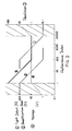
- an optical displacement measuring system of the first embodiment comprises a light projecting unit 1 for emitting a laser beam, which is amplitude-modulated by a reference signal having a predetermined period, to an object OBJ , and a light receiving unit 2 for receiving light reflected back from the object.
- the projecting unit 1 includes a laser diode 13 and a first lens 14 .
- the period of the reference signal can be determined in a range of 10 kHz to 200 kHz. Therefore, a light output of the modulated laser beam is varied with respect to time.
- the reference signal is generated by an oscillator 10 , and then sent to a control signal generator 35 to output a control signal t 2 in synchronism with the reference signal, as shown in FIG. 2G.
- the period of the reference signal is equal to that of the control signal t 2 .
- the control signal t 2 is input as a carrier to a modulator 11 at which an amplitude modulation of the carrier is performed according to an output of a feed-back unit 6 explained later. Therefore, a peak-to-peak amplitude of the modulated laser beam can be adjusted in response to the output of the feed-back unit 6 .
- the reference signal may be directly sent from the oscillator 10 to a laser-diode driving circuit 12 to emit the modulated laser beam from the laser diode 13 .
- An output of the modulator 11 is sent to the laser-diode driving circuit 12 to emit the modulated laser beam from the laser diode 13 .
- the emitted laser beam makes a light spot P on the object OBJ .
- the receiving unit comprises a second lens 20 and position sensitive device 21 (PSD) for receiving the reflected light from the light spot P .
- PSD 21 position sensitive device 21
- the PSD 21 is a semiconductor element having a "pin" structure which has a common electrode and a pair of electrodes disposed at opposite ends of a light sensitive surface of the PSD 21 . An electric resistance between the electrodes is divided by a position of a light spot formed on the light sensitive surface.
- the electrodes of the PSD 21 respectively output the position signals I 1 and I 2 .
- a displacement between the light spot P on the object OBJ and a standard position S can be determined by the use of the position signals I 1 and I 2 .
- the standard position S is on the axis of the laser beam emitted from the laser diode 13 , as shown in FIG. 1, and can be determined such that light reflected back from the standard position S is received at the center of an effective length of the PSD 21 .
- a period of each of the position signals I 1 and I 2 is equal to the period of the control signal t 2 .
- the position signals I 1 and I 2 are current signals, they are converted into voltage signals Va 1 and Va 2 by I/V converters 30 and 31 , respectively.
- the voltage signals Va 1 and Va 2 are sent to a first operating unit 32 at which a difference between the signals Va 1 and Va 2 is calculated.
- the first operating unit 32 outputs the signal Va 2 and a first operation signal Va 1 -Va 2 .
- the signals Va 1 -Va 2 and Va 2 are processed by a first switching circuit 33 in a time sharing manner according to a first control signal t 1 to obtain a first composite signal Va in which the signals Va 1 -Va 2 and Va 2 occur alternately every one period of the reference signal, as shown in FIG. 2C.
- one-period component of the signal Va 1 -Va 2 is extracted at a level H of the control signal t 1
- one-period component of the signal Va 2 is extracted at a level L of the control signal t 1
- the first control signal t 1 is generated by the control signal generator 35 , and sent to the first switching circuit 33 . Since the first control signal t 1 is synchronized with the reference signal, the first composite signal of FIG. 2C can be obtained. In this embodiment, the period of the control signal t 1 is two times as long as the period of the control signal t 2 .
- the first composite signal Va is amplified by an amplifier 34 at a desired amplification rate, and then is input into a detector 40 .
- the first composite signal Va is processed according to the control signal t 2 to obtain a second composite signal Vd , in which the first composite signal Va is polarity-reversed every half period of the reference signal, as shown in FIG. 2E. That is, the polarity of the first composite signal Va is not reversed at a level H of the control signal t 2 shown in FIG. 2D, but is reversed at a level L of the control signal t 2 .
- the second composite signal Vd is divided into a pair of pulse signals Vd 1 -Vd 2 and Vd 2 according to the control signal t 1 by a second switching circuit 36 , as shown in FIGS. 2G and 2H. That is, only signal component Vd 1 -Vd 2 of the second composite signal Vd is extracted at the level H of the control signal t 1 , and only signal component Vd 2 of the second composite signal Vd is extracted at the level L of the control signal t 1 .
- the pulse signals Vd 1 -Vd 2 and Vd 2 are sent to a second operating unit 5 .
- the second operating unit 5 comprises a first low-pass filter 51 for integrating the pulse signal Vd 1 -Vd 2 to provide a signal V 1 -V 2 , a second low-pass filter 52 for integrating the pulse signal Vd 2 to provide a signal V 2 , and an adder circuit 53 for calculating an operational signal V 1 +k ⁇ V 2 by using the signals V 1 -V 2 and V 2 .
- the value k is a constant for nonlinearity correction.
- a distance signal indicative of the displacement between the light spot P on the object OBJ and the standard position S is given by dividing the signal V 1 -V 2 by the operational signal V 1 +k ⁇ V 2 .
- the operational signal V 1 +k ⁇ V 2 can be maintained at a constant value by the feed-back unit 6 , only the signal V 1 -V 2 provided from the low-pass filter 51 can be used as the distance signal.
- a divider circuit for dividing the signal V 1 -V 2 by the operational signal V 1 +k ⁇ V 2 is necessary to obtain the distance signal.
- the output V 1 +k ⁇ V 2 of the adder circuit 53 means a total amount of light energy received by the PSD 21 .
- the output V 1 +k ⁇ V 2 of the adder circuit 53 is compared with a reference voltage Vref by an error amplifier 60 to provide an analog voltage signal indicative of a difference between an amount of light energy determined by the reference voltage Vref and the amount of light energy actually received by PSD 21 .
- the analog voltage signal of the error amplifier 60 the light output of the modulated laser beam emitted from the laser diode 13 and the amplification rate of the amplifier 34 are controlled by a feed-back control circuit 61 such that the actual light energy is maintained at the reference light energy.
- the light output and the amplification rate are controlled in a feed-back manner such that when the actual light energy is smaller than the reference light energy, the amplification rate is increased, and when the actual light energy is larger than the reference light energy, the light output is decreased.
- Adjustable ranges of the light output of the modulated laser beam and the amplification rate are in a range of 1 % to 100 %, respectively.
- Reflectance index is defined herein to be 100 when the PSD 21 receives a predetermined intensity of light reflected from a standard object, e.g., a white ceramic, which is located at fixed distances from the light projecting unit 1 as well as the light receiving unit 2 .
- the reflectance index is 100
- the light output of the modulated laser beam and the amplification rate are adjusted to 100 % and 1 %, respectively. In this situation, as the reflectance index is larger than 100, the light output of the modulated laser beam is reduced, as shown by the line 1 of FIG.
- the line 3 designates a resolution of the optical displacement measuring system
- the line 4 designates a voltage value corresponding to the amount of light energy received by the PSD 21 .
- the voltage value is maintained constant within a range of the reflectance index of 1 to 10000.
- a standard value the reflectance index is set at 100, however, it may be adequately set, if necessary.
- the standard value of the reflectance index may be set at 10, so that the feed-back manner is available within a range of the reflectance index of 0.1 to 1000.
- the signals Va 1 -Va 2 and Va 2 are processed by the first switching circuit 33 according to the first control signal t 1 to obtain the first composite signal Va in which the signals Va 1 -Va 2 and Va 2 occur alternately every one period of the reference signal.
- an optical displacement measuring system of the second embodiment comprises a light projecting unit 1A for emitting a laser beam, which is amplitude-modulated by a reference signal having a predetermined period, to an object OBJ , and a light receiving unit 2A for receiving light reflected back from the object OBJ .
- the projecting unit 1A includes a laser diode 13A and a first lens 14A .
- the reference signal is generated by an oscillator 10A , and then sent to a laser-diode driving circuit 12A to emit the modulated laser beam from the laser diode 13A .
- the modulated laser beam makes a light spot P on the object OBJ .
- the receiving unit 2A comprises a second lens 20A and a position sensitive device 21A (PSD) for receiving the reflected light from the light spot P .
- PSD 21A position sensitive device 21A
- the PSD 21A receives the reflected beam through the second lens 20A , it provides a pair of position signals I 1 and I 2 , as shown in FIG. 5A and 5B.
- a period of each of the position signals I 1 and I 2 is equal to the period of the reference signal.
- the position signals I 1 and I 2 are processed by a switching circuit 33A in a time sharing manner according to a first control signal t 1 in synchronism with the reference signal to obtain a first composite signal Ia in which the signals I 1 and I 2 occurs alternately every one period of the reference signal, as shown in FIG. 5C. That is, one-period component of the signal I 1 is extracted at a level H of the control signal t 1 shown in FIG. 5I, and on the other hand, one-period component of the signal I 2 is extracted at a level L of the control signal t 1 .
- the control signal t 1 is provided from a control signal generator 35A which is connected to the oscillator 10A . Since the first control signal t 1 is synchronized with the reference signal, the first composite signal Ia shown in FIG. 5C can be obtained. In this embodiment, the period of the control signal t 1 is two times as long as the period of the reference signal.
- the first composite signal Ia is a current signal, it is converted into a voltage signal Va by an I/V converter 30A . Therefore, the signal Va is a composite voltage signal, in which signal components Va 1 and Va 2 occur alternately every one period of the reference signal, as shown in FIG. 5D.
- the signal Va is amplified by an amplifier 34A at a desired amplification rate, and then is sent to a detector 40A .
- the composite signal Va is processed according to a control signal t 2 in synchronism with the reference signal such that the composite signal Va is polarity-reversed every half period of the reference signal to obtain a second composite signal, as shown in FIG. 5H.
- the polarity of the composite signal Va is not reversed at a level H of the control signal t 2 shown in FIG. 5G, but is reversed at a level L of the control signal t 2 .
- the control signal t 2 is provided from the control signal generator 35A .
- a period of the control signal t 2 is the same as that of the reference signal. Since the control signal t 2 is synchronized with the reference signal, the second composite signal can be obtained.
- signal components +Vd 1 and +Vd 2 occur alternately every one period of the reference signal in the second composite signal. Therefore, the second composite signal is shown as Vd 1 +Vd 2 .
- the composite signal Va is also processed according to a third control signal t 3 in synchronism with the reference signal such that the composite signal Va is polarity-reversed every one period of the reference signal to obtain a third composite signal, as shown in FIG. 5F. That is, the polarity of the composite signal Va is not reversed at a level H of the control signal t 3 shown in FIG. 5E, but is reversed at a level L of the control signal t 3 .
- the control signal t 3 provided from the control signal generator 35A has the same period as the control signal t 1 , but is in out of phase relation to the control signal t 1 by 90 degrees.
- signal components +Vd 1 and -Vd 2 occur alternately every one period of the reference signal in the third composite signal. Therefore, the third composite signal is shown as Vd 1 -Vd 2 .
- the composite signals Vd 1 +Vd 2 and Vd 1 -Vd 2 are sent to an operating unit 5A comprising a first low-pass filter 51A for integrating the composite signal Vd 1 -Vd 2 to provide a signal V 1 -V 2 , a second low-pass filter 52A for integrating the composite signal Vd 1 +Vd 2 to provide a signal V 1 +V 2 , and a divider circuit 54A for dividing the signal V 1 -V 2 by the signal V 1 +V 2 .
- An output of the divider circuit 54A i.e., (V 1 -V 2 ) / (V 1 +V 2 ) , is used as a distance signal indicative of the displacement between the light spot P on the object OBJ and a standard position S .
- the divider circuit 54A since only one switching circuit 33A is used, it is possible to decrease the occurrence of switching noises to improve the accuracy of measurement.
- the detector 40A has a first circuit 41A for providing the composite signal Vd 1 -Vd 2 and a second circuit 42A for providing the composite signal Vd 1 +Vd 2 , as shown in FIG. 6.
- the first circuit 41A has an operational amplifier OP1 for non-inverting and amplifying the composite signal Va , an operational amplifier OP2 for inverting and amplifying the composite signal Va , and a switch S1 for switching outputs of the operational amplifiers OP1 and OP2 according to the control signal t 3 to provide the composite signal Vd 1 -Vd 2 .
- the second circuit 42A has an operational amplifier OP3 for non-inverting and amplifying the composite signal Va , an operational amplifier OP4 for inverting and amplifying the composite signal Va , and a switch S2 for switching outputs of the operational amplifiers OP3 and OP4 according to the control signal t 2 to provide the composite signal Vd 1 +Vd 2 .
- a detector 40A' can be used in place of the detector 40A .
- Waveforms of FIGS. 7A to 7D are the same as those of FIGS. 5A to 5D.
- the composite signal Va is processed according to the third control signal t3 such that the composite signal Va is polarity-reversed alternately every one period of the reference signal to obtain a second composite signal, as shown in FIG. 7F. That is, the polarity of the composite signal Va is not reversed at a level H of the control signal t3 shown in FIG. 7E, but is reversed at a level L of the control signal t3 .
- signal components +Vd 1 and -Vd 2 occur alternately every one period of the reference signal in the second composite signal. Therefore, the second composite signal is shown as Vd 1 -Vd 2 .
- the composite signal Vd 1 -Vd 2 is then processed according to the control signal t 1 such that the composite signal Vd 1 -Vd 2 is polarity-reversed every one period of the reference signal to obtain a third composite, as shown in FIG. 7H. That is, the signal component +Vd 1 of the second composite signal Vd 1 -Vd 2 is not polarity-reversed at a level H of the control signal t 1 shown in FIG. 7G. On the other hand, at a level L of the control signal t 1 , the signal component -Vd 2 of the composite signal Vd 1 -Vd 2 is polarity-reversed. As shown in FIG. 7H, signal components +Vd 1 and +Vd 2 occur alternately every one period of the reference signal in the third composite signal. Therefore, the third composite signal is shown as Vd 1 +Vd 2 .
- the detector 40A' has a first circuit 41A' for providing the composite signal Vd 1 -Vd 2 and a second circuit 42A' for providing the composite signal Vd 1 +Vd 2 , as shown in FIG. 8.
- the first circuit 41A' has an operational amplifier OP1 for non-inverting and amplifying the composite signal Va , an operational amplifier OP2 for inverting and amplifying the composite signal Va , and a switch S1 for switching outputs of the operational amplifiers OP1 and OP2 according to the control signal t3 to provide the composite signal Vd 1 -Vd 2 .
- the second circuit 42A' has an operational amplifier OP3 for non-inverting and amplifying the composite signal Vd 1 -Vd 2 , an operational amplifier OP4 for inverting and amplifying the composite signal Vd 1 -Vd 2 , and a switch S2 for switching outputs of the operational amplifiers OP3 and OP4 according to the control signal t 1 to provide the composite signal Vd 1 +Vd 2 .
- a detector 40A'' can be used in place of the detector 40A .
- Waveforms of FIGS. 9A to 9D are the same as those of FIGS. 5A to 5D.
- the composite signal Va is processed according to the control signal t 2 such that the composite signal Va is polarity-reversed every half period of the reference signal to obtain a second composite signal, as shown in FIG. 9F. That is, the polarity of the composite signal Va is not reversed at a level H of the control signal t 2 shown in FIG. 9E, but is reversed at a level L of the control signal t 2 .
- signal components +Vd 1 and +Vd 2 occur alternately every one period of the reference signal in the second composite signal. Therefore, the second composite signal is shown as Vd 1 +Vd 2 .
- the composite signal Vd 1 +Vd 2 is processed according to the control signal t 1 such that the composite signal Vd 1 +Vd 2 is polarity-reversed every one period of the reference signal to obtain a third composite signal, as shown in FIG. 9H. That is, the signal component Vd 1 of the composite signal Vd 1 +Vd 2 is not polarity-reversed at a level H of the control signal t 1 shown in FIG. 9G. On the other hand, at a level L of the control signal t 1 , the signal component Vd 2 of the composite signal Vd 1 +Vd 2 is polarity-reversed. As shown in FIG. 9H, signal components +Vd 1 and -Vd 2 occur alternately every one period of the reference signal in the third composite signal. Therefore, the third composite signal is shown as Vd 1 -Vd 2 .
- the detector 40A'' has a first circuit 41A'' for providing the composite signal Vd 1 +Vd 2 and a second circuit 42A'' for providing the composite signal Vd 1 -Vd 2 , as shown in FIG. 10.
- the first circuit 41A'' has an operational amplifier OP1 for non-inverting and amplifying the composite signal Va , an operational amplifier OP2 for inverting and amplifying the composite signal Va , and a switch S1 for switching outputs of the operational amplifiers OP1 and OP2 according to the control signal t 2 to provide the composite signal Vd 1 +Vd 2 .
- the second circuit 42A'' has an operational amplifier OP3 for non-inverting and amplifying the composite signal Vd 1 +Vd 2 , an operational amplifier OP4 for inverting and amplifying the composite signal Vd 1 +Vd 2 , and a switch S2 for switching outputs of the operational amplifiers OP3 and OP4 according to the control signal t 1 to provide the composite signal Vd 1 -Vd 2 .
- adder and subtracter circuits are not needed in the operating unit 5A by using any one of the detectors 40A , 40A' and 40A'' , it is possible to simplify components parts of the operating unit 5A , while eliminating a problem of the occurrence of operation errors at the adder and subtracter circuits.
- an optical displacement measuring system of the third embodiment comprises a projecting unit 1B for emitting a laser beam, which is amplitude-modulated by a reference signal having a predetermined period, to an object OBJ , and a receiving unit 2B for receiving light reflected back from the object.
- the projecting and receiving units 1B and 2B are substantially same as those of the first embodiment. Therefore, no duplicate explanation to common parts and operation is deemed necessary.
- Like parts are designated by like numerals with a suffixed letter of B .
- the PSD ( 21 and 21A ) receives only the reflected light from the object OBJ .
- a position sensitive device (PSD) 21B receives the influence of disturbance light. That is, direct-current components DC1 and DC2 are included in a pair of position signals I 1 and I 2 provided from the PSD 21B , respectively, as shown in FIGS. 12A and 12B.
- the signals I 1 and I 2 are processed by a first switching circuit 33B in a time sharing manner according to a first control signal t 1 in synchronism with the reference signal to obtain a first composite signal Ia in which the position signals I 1 and I 2 occur alternately every one period of the reference signal, as shown in FIG. 12C. That is, one-period component of the position signal I 1 is extracted at a level L of the control signal t 1 shown in FIG. 12G and one-period component of the signal I 2 is extracted at a level H of the control signal t 1 . Since the first control signal t 1 is synchronized with the reference signal, the composite signal Ia can be obtained.
- the control signal t 1 is provided from a control signal generator 35B .
- the period of the control signal t 1 is two times as long as the period of the reference signal.
- the direct-current components DC1 and DC2 in the position signals I 1 and I 2 are mixed by the first switching circuit 33B , so that the composite signal Ia contains a difference of the direct current components DC1-DC2 , as shown in FIG. 12C.
- the composite signal Ia is converted into a voltage signal Va by an I/V converter 30B . Therefore, the signal Va is a composite voltage signal, in which signal components Va 1 and Va 2 occur alternately every one period of the reference signal, as shown in FIG. 12D. In addition, the signal Va contains a difference of offset voltage Vdc 1 -Vdc 2 corresponding to the difference of the direct current components DC1-DC2 .
- the signal Va is amplified at a desired amplification rate by an amplifier 34B , and then input into a detector 40B .
- the signal Va is processed according to a control signal t 2 in synchronism with the reference signal to obtain a second composite signal Vb , in which the signal Va is polarity-reversed every half period of the reference signal, as shown in FIG. 12F. That is, the polarity of the signal Va is not reversed at a level H of the control signal t 2 shown in FIG. 12E, but is reversed at a level L of the control signal t 2 .
- a period of the control signal t 2 is the same as the period of the reference signal. As shown in FIG.
- signal components Vb 1 and Vb 2 occur alternately every one period of the reference signal in the composite signal Vb .
- offset-cancel voltages -Vdc 1 and -Vdc 2 having the opposite polarity of the offset voltages Vdc 1 and Vdc 2 in the signal Va are generated by the detector 40B , and are contained in the signal components Vb 1 and Vb 2 of the composite signal Vb , respectively.
- the composite signal Vb is divided into a pair of pulse signals Vd 1 and Vd 2 in a time sharing manner according to the control signal t 1 by a second switching circuit 36B , as shown in FIG. 12H and 12I. That is, only the signal component Vb 1 of the composite signal Vb is extracted at the level L of the control signal t 1 to obtain the pulse signal Vd 1 . Similarly, only the signal component Vb 2 of the composite signal Vb is extracted at the level H of the control signal t 1 to obtain the pulse signal Vd 2 .
- the pulse signals Vd 1 and Vd 2 are sent to an operating unit 5B comprising a first low-pass filter 51B for integrating the pulse signal Vd 1 to provide a signal V 1 , a second low-pass filter 52B for integrating the pulse signal Vd 2 to provide a signal V 2 , and an adder 53B for calculating a sum of the signals V 1 and V 2 , and a subtracter 55B for calculating a difference between the signals V 1 and V 2 .
- the pulse signal Vd 1 is integrated by the low-pass filter 51B
- the offset voltage Vdc 1 is canceled by the offset-cancel voltage -Vdc 1 .
- an output V 1 +V 2 of the adder 53B is controlled by a feed-back unit 6B in the same manner as the first embodiment, an output V 1 -V 2 of the subtracter 54B can be used as a distance signal indicative of the displacement between the light spot P on the object OBJ and a standard position S .
- a divider circuit for dividing the output V 1 -V 2 by the output V 1 +V 2 is necessary to obtain the distance signal.
- the present system can remove the noise components, i.e., the direct-current components DC1 and DC2 , from the distance signal indicative of the displacement to improve the accuracy of measurement.
- the position signals I 1 and I 2 are processed by the first switching circuit 33B according to the first control signal t 1 to obtain the composite signal Ia in which the position signals I 1 and I 2 occur alternately every one period of the reference signal, as shown in FIG. 12C.
- the position signals I 1 and I 2 may be processed in a time sharing manner according to a control signal t 1' to obtain a composite signal I a' in which the position signals I 1 and I 2 occur alternately every three-times period of the reference signal.
- a period of the control signal t 1' is six times as long as the period of the reference signal.
- an optical displacement measuring system of the fourth embodiment comprises a light projecting unit 1C for emitting a laser beam, which is amplitude-modulated by a reference signal having a predetermined period, to an object OBJ , and a light receiving unit 2C for receiving light reflected back from the object.
- the projecting and receiving units 1C and 2C are substantially same as those of the second embodiment. Therefore, no duplicate explanation to common parts and operation is deemed necessary.
- Like parts are designated by like numerals with a suffixed letter of C .
- a pair of position signals I 1 and I 2 are provided from a position sensitive device (PSD) 21C .
- the position signals I 1 and I 2 are converted into voltage signals Va 1 and Va 2 (not shown) by I/V converters 30C and 31C , respectively.
- the voltage signals Va 1 and Va 2 are sent to a first operating unit 32C to calculate a difference between the voltage signals Va 1 and Va 2 and a sum of the voltage signals Va 1 and Va 2 . Therefore, the first operating unit 32C provides output signals Va 1 -Va 2 and Va 1 +Va 2 .
- the signals Va 1 -Va 2 and Va 1 +Va 2 are processed by a switching circuit 33C in a time sharing manner according to a first control signal t 1 in synchronism with the reference signal to obtain a first composite signal Va in which the signals Va 1 -Va 2 and Va 1 +Va 2 occur alternately every one period of the reference signal, as shown in FIG. 15C. That is, one-period component of the signal Va 1 +Va 2 is extracted at a level H of the control signal t 1 shown in FIG. 15F, and on the other hand one-period component of the signal Va 1 -Va 2 is extracted at a level L of the control signal t 1 .
- the control signal t 1 is provided from a control signal generator 35C . Since the first control signal t 1 is synchronized with the reference signal, the composite signal Va can be obtained. The period of the control signal t 1 is two times as long as the period of the reference signal.
- the composite signal Va is amplified by an amplifier 34C at a desired amplification rate, and then sent to a detector 40C .
- the composite signal Va is processed according to a control signal t 2 in synchronism with the reference signal such that the composite signal Va is polarity-reversed every one period of the reference signal to obtain a second composite signal Vd , as shown in FIG. 15E. That is, the polarity of the composite signal Va is not reversed at a level H of the control signal t 2 shown in FIG. 15D, but is reversed at a level L of the control signal t 2 .
- the control signal t 2 provided from the control signal generator 35C has the same period as the control signal t 1 , but is in out of phase relation to the control signal t 1 by 90 degrees.
- signal components Vd 1 +Vd 2 and Vd 2 -Vd 1 occurs alternately every one period of the reference signal in the composite signal Vd .
- the composite signal Vd is processed according to the control signal t 1 such that only the signal component Vd 2 -Vd 1 is polarity-reversed, and then extracted to provide a pulse signal Vd 1 -Vd 2 , as shown in FIG. 15G.
- the composite signal Vd is integrated to provide a signal Vd 2 (not shown).
- the detector 40C outputs the signals Vd 1 -Vd 2 and Vd 2 .
- the signal Vd 1 -Vd 2 and Vd 2 are sent to a second operating unit 5C comprising a first low-pass filter 51C for integrating the signal Vd 1 -Vd 2 to provide a signal V 1 -V 2 , a second low-pass filter 52C for integrating the signal Vd 2 to provide a signal V 2 , an adder circuit 53C for calculating a signal V 1 +k ⁇ V 2 by the use of the signals V 1 -V 2 and V 2 , and a divider circuit 54C for dividing the signal V 1 -V 2 by the signal V 1 +k ⁇ V 2 .
- a distance signal indicative of a displacement between a light spot P on the object OBJ and a standard position S is determined by the following expression, i.e., ( V 1 -V 2 ) / ( V 1 +k ⁇ V 2 ) .
- the first operating unit 32C provides the output signals Va 1 -Va 2 and Va 1 +Va 2 .
- another operating unit for providing output signals Va 1 and Va 1 -Va 2 may be used in place of the first operating unit 32C .
- an optical displacement measuring system of the fourth embodiment comprises a light projecting unit 1D for emitting a laser beam, which is amplitude-modulated by a reference signal having a predetermined period, to an object OBJ , and a light receiving unit 2D for receiving light reflected back from the object.
- the projecting and receiving units 1D and 2D are substantially same as those of the second embodiment. Therefore, no duplicate explanation to common parts and operation is deemed necessary.
- Like parts are designated by like numerals with a suffixed letter of D .
- a pair of position signals I 1 and I 2 are provided from a position sensitive device (PSD) 21D .
- the position signals I 1 and I 2 are amplitude-modulated by the influence of noises.
- the position signal I 1 is equal to the position signal I 2 . It means that light reflected back from the object OBJ makes a light spot at the center of an effective length of the PSD 21D .
- the object OBJ is usually set in the vicinity of the center of the effective length because the center of the effective length of the PSD 21D can provide good response characteristic, and also the occurrence of errors according to a beam size of the laser beam can be suppressed.
- the position signals I 1 and I 2 are converted into voltage signals Va 1 and Va 2 (not shown) by I/V converters 30D and 31D , respectively.
- the voltage signals Va 1 and Va 2 are sent to a first operating unit 32D to calculate a difference between the voltage signals Va 1 and Va 2 and a sum of the voltage signals Va 1 and Va 2 . Therefore, the first operating unit 32D provides output signals Va 1 -Va 2 and Va 1 +Va 2 . Since the voltage signals Va 1 and Va 2 are processed by the first operating unit 32D before being sent to a first switching unit 33D , common noise components in the voltage signals Va 1 and Va 2 can be removed.
- the output signals Va 1 -Va 2 and Va 1 +Va 2 are processed by the first switching circuit 33D in a time sharing manner according to a first control signal t 1 in synchronism with the reference signal to obtain a first composite signal Va in which the signals Va 1 -Va 2 and Va 1 +Va 2 occur alternately every one period of the reference signal, as shown in FIG. 17C. That is, one-period component of the signal Va 1 +Va 2 is extracted at a level H of the control signal t 1 shown in FIG. 17F, and one-period component of the signal Va 1 -Va 2 is extracted at a level L of the control signal t 1 . In this embodiment, the signal Va 1 -Va 2 is zero.
- the control signal t 1 is provided from a control signal generator 35D . Since the control signal t 1 is synchronized with the reference signal, the composite signal Va can be obtained. The period of the control signal t 1 is two times as long as the period of the reference signal.
- the composite signal Va is amplified by an amplifier 34D at a desired amplification rate, and then sent to a detector 40D .
- the composite signal Va is processed according to a control signal t 2 in synchronism with the reference signal to obtain a second composite signal Vd , in which the composite signal Va is polarity-reversed every half period of the reference signal, as shown in FIG. 17E. That is, the polarity of the composite signal Va is not reversed at a level H of the control signal t 2 shown in FIG. 17D, but is reversed at a level L of the control signal t 2.
- signal components Vd 1 +Vd 2 and Vd 1 -Vd 2 occur alternately every one period of the reference signal in the composite signal Vd .
- a period of the control signal t 2 is the same as the period of the reference signal.
- the pulse signals Vd 1 +Vd 2 and Vd 1 -Vd 2 are sent to a second operating unit 5D comprising a first low-pass filter 51D for integrating the pulse signal Vd 1 -Vd 2 to provide a signal V 1 -V 2 , a second low-pass filter 52D for integrating the pulse signal Vd 1 +Vd 2 to provide a signal V 1 +V 2 , and a divider 54D for dividing the signal V 1 -V 2 by the signal V 1 +V 2 to provide a distance signal indicative of a displacement between a light spot P on the object OBJ and a standard position S . Therefore, the distance signal is determined by the following expression, i.e., ( V 1 - V 2 )/( V 1 +V 2 ) .
- the voltage signals Va 1 and Va 2 are input into the first operating unit 32D , therefore, it is required that the current signals I 1 and I 2 provided from the PSD 21D are converted into the voltage signals Va 1 and Va 2 by the I/V converters 30D and 31D .
- the first and second operating unit 32D and 5D are modified to receive the current signals I 1 and I 2 , it is possible to eliminate the use of the I/V converters 30D and 31D from this displacement measuring system.
Landscapes
- Physics & Mathematics (AREA)
- Electromagnetism (AREA)
- Engineering & Computer Science (AREA)
- General Physics & Mathematics (AREA)
- Radar, Positioning & Navigation (AREA)
- Remote Sensing (AREA)
- Computer Networks & Wireless Communication (AREA)
- Optics & Photonics (AREA)
- Measurement Of Optical Distance (AREA)
- Length Measuring Devices By Optical Means (AREA)
Applications Claiming Priority (9)
| Application Number | Priority Date | Filing Date | Title |
|---|---|---|---|
| JP219332/95 | 1995-08-28 | ||
| JP21933295A JP3627308B2 (ja) | 1995-08-28 | 1995-08-28 | 光学式変位測定装置 |
| JP21933295 | 1995-08-28 | ||
| JP157679/96 | 1996-05-28 | ||
| JP157680/96 | 1996-05-28 | ||
| JP15768096A JP3661279B2 (ja) | 1996-05-28 | 1996-05-28 | 光学式変位測定装置 |
| JP15767996 | 1996-05-28 | ||
| JP15768096 | 1996-05-28 | ||
| JP15767996A JP3661278B2 (ja) | 1996-05-28 | 1996-05-28 | 光学式変位測定装置 |
Publications (3)
| Publication Number | Publication Date |
|---|---|
| EP0760460A2 true EP0760460A2 (fr) | 1997-03-05 |
| EP0760460A3 EP0760460A3 (fr) | 1998-05-20 |
| EP0760460B1 EP0760460B1 (fr) | 2002-07-03 |
Family
ID=27321215
Family Applications (1)
| Application Number | Title | Priority Date | Filing Date |
|---|---|---|---|
| EP96113702A Expired - Lifetime EP0760460B1 (fr) | 1995-08-28 | 1996-08-27 | Système optique de mesure de déplacement utilisant triangulation |
Country Status (4)
| Country | Link |
|---|---|
| US (1) | US5814808A (fr) |
| EP (1) | EP0760460B1 (fr) |
| KR (1) | KR100256710B1 (fr) |
| DE (1) | DE69622103T2 (fr) |
Cited By (2)
| Publication number | Priority date | Publication date | Assignee | Title |
|---|---|---|---|---|
| EP1243944A3 (fr) * | 2001-03-19 | 2004-10-27 | Matsushita Electric Works, Ltd. | Dispositif de mesure à distance |
| WO2006118286A1 (fr) | 2005-05-02 | 2006-11-09 | Matsushita Electric Works, Ltd. | Dispositif de detection d’informations concernant l’espace, et systeme de detection d’informations concernant l’espace utilisant le dispositif |
Families Citing this family (33)
| Publication number | Priority date | Publication date | Assignee | Title |
|---|---|---|---|---|
| JP3799708B2 (ja) * | 1996-12-24 | 2006-07-19 | 松下電工株式会社 | 光学式変位測定システム |
| US8412377B2 (en) | 2000-01-24 | 2013-04-02 | Irobot Corporation | Obstacle following sensor scheme for a mobile robot |
| US8788092B2 (en) | 2000-01-24 | 2014-07-22 | Irobot Corporation | Obstacle following sensor scheme for a mobile robot |
| US6956348B2 (en) | 2004-01-28 | 2005-10-18 | Irobot Corporation | Debris sensor for cleaning apparatus |
| US6690134B1 (en) | 2001-01-24 | 2004-02-10 | Irobot Corporation | Method and system for robot localization and confinement |
| US7571511B2 (en) | 2002-01-03 | 2009-08-11 | Irobot Corporation | Autonomous floor-cleaning robot |
| US7429843B2 (en) | 2001-06-12 | 2008-09-30 | Irobot Corporation | Method and system for multi-mode coverage for an autonomous robot |
| US8396592B2 (en) | 2001-06-12 | 2013-03-12 | Irobot Corporation | Method and system for multi-mode coverage for an autonomous robot |
| US9128486B2 (en) | 2002-01-24 | 2015-09-08 | Irobot Corporation | Navigational control system for a robotic device |
| KR20030095629A (ko) * | 2002-06-12 | 2003-12-24 | 최병국 | 양면 합포 방법 및 양면 합포기 |
| US8428778B2 (en) | 2002-09-13 | 2013-04-23 | Irobot Corporation | Navigational control system for a robotic device |
| US8386081B2 (en) | 2002-09-13 | 2013-02-26 | Irobot Corporation | Navigational control system for a robotic device |
| DK1528411T3 (da) * | 2003-10-27 | 2010-05-17 | Bea Sa | Sensor til afstandsmåling |
| US7332890B2 (en) | 2004-01-21 | 2008-02-19 | Irobot Corporation | Autonomous robot auto-docking and energy management systems and methods |
| WO2006002385A1 (fr) | 2004-06-24 | 2006-01-05 | Irobot Corporation | Outil de programmation et de diagnostic pour robot mobile |
| US8972052B2 (en) | 2004-07-07 | 2015-03-03 | Irobot Corporation | Celestial navigation system for an autonomous vehicle |
| US7706917B1 (en) | 2004-07-07 | 2010-04-27 | Irobot Corporation | Celestial navigation system for an autonomous robot |
| KR101247933B1 (ko) | 2005-02-18 | 2013-03-26 | 아이로보트 코퍼레이션 | 습식 및 건식 청소를 위한 자동 표면 청소 로봇 |
| US7620476B2 (en) | 2005-02-18 | 2009-11-17 | Irobot Corporation | Autonomous surface cleaning robot for dry cleaning |
| US8392021B2 (en) | 2005-02-18 | 2013-03-05 | Irobot Corporation | Autonomous surface cleaning robot for wet cleaning |
| US8930023B2 (en) | 2009-11-06 | 2015-01-06 | Irobot Corporation | Localization by learning of wave-signal distributions |
| WO2007065034A1 (fr) | 2005-12-02 | 2007-06-07 | Irobot Corporation | Robot modulaire |
| EP2816434A3 (fr) | 2005-12-02 | 2015-01-28 | iRobot Corporation | Robot à couverture autonome |
| ES2706729T3 (es) | 2005-12-02 | 2019-04-01 | Irobot Corp | Sistema de robot |
| KR101099808B1 (ko) | 2005-12-02 | 2011-12-27 | 아이로보트 코퍼레이션 | 로봇 시스템 |
| EP2251757B1 (fr) | 2005-12-02 | 2011-11-23 | iRobot Corporation | Mobilité de robot de couverture |
| ES2583374T3 (es) | 2006-05-19 | 2016-09-20 | Irobot Corporation | Eliminación de residuos de robots de limpieza |
| US8417383B2 (en) | 2006-05-31 | 2013-04-09 | Irobot Corporation | Detecting robot stasis |
| EP2574265B1 (fr) | 2007-05-09 | 2015-10-14 | iRobot Corporation | Robot autonome de couverture compact |
| EP2040427A1 (fr) * | 2007-09-22 | 2009-03-25 | New Day Investment Limited | Système de transmission de données électriques à haute vitesse |
| US8800107B2 (en) | 2010-02-16 | 2014-08-12 | Irobot Corporation | Vacuum brush |
| JP6040542B2 (ja) * | 2012-03-15 | 2016-12-07 | オムロン株式会社 | 受光用集積回路およびこの集積回路を用いた光電センサ |
| US9201145B2 (en) | 2013-10-17 | 2015-12-01 | Globalfoundries Inc. | Object location in three dimensional space using LED lights |
Family Cites Families (16)
| Publication number | Priority date | Publication date | Assignee | Title |
|---|---|---|---|---|
| JPS6110711A (ja) * | 1984-06-27 | 1986-01-18 | Matsushita Electric Ind Co Ltd | 光式距離測定装置 |
| JPS61112902A (ja) * | 1984-11-07 | 1986-05-30 | Riide Denki Kk | 非接触変位測定装置 |
| US4758082A (en) * | 1985-04-17 | 1988-07-19 | Canon Kabushiki Kaisha | Distance detection apparatus |
| US4761546A (en) * | 1985-11-25 | 1988-08-02 | Matsushita Electric Works, Ltd. | Optical displacement measuring system with nonlinearity correction |
| US5047793A (en) * | 1985-12-26 | 1991-09-10 | Canon Kabushiki Kaisha | Automatic range finder camera system with a remote control function |
| US4855585A (en) * | 1986-11-21 | 1989-08-08 | Olympus Optical Co., Ltd. | Distance measuring apparatus |
| JP2704958B2 (ja) * | 1988-02-27 | 1998-01-26 | キヤノン株式会社 | 測距装置 |
| JPH01254807A (ja) * | 1988-04-04 | 1989-10-11 | Canon Inc | 測距装置 |
| JPH02118402A (ja) * | 1988-10-28 | 1990-05-02 | Toshiba Corp | 高精度位置測定回路 |
| JPH02118408A (ja) * | 1988-10-28 | 1990-05-02 | Mitsubishi Heavy Ind Ltd | 鋼構造物部材のキヤンバー量検出方法 |
| JPH0714970Y2 (ja) * | 1988-12-29 | 1995-04-10 | 株式会社精工舎 | 自動焦点調整装置 |
| JP2684574B2 (ja) * | 1989-10-03 | 1997-12-03 | キヤノン株式会社 | 測距装置 |
| US5157435A (en) * | 1990-09-29 | 1992-10-20 | Samsung Electronics Co., Ltd. | Automatic focusing apparatus for a video camera and the method thereof |
| US5351126A (en) * | 1991-10-31 | 1994-09-27 | Matsushita Electric Works, Ltd. | Optical measurement system for determination of an object's profile or thickness |
| US5444511A (en) * | 1992-10-29 | 1995-08-22 | Seikosha Co., Ltd. | Distance measuring device for camera |
| US5572012A (en) * | 1993-06-16 | 1996-11-05 | Seiko Precision Inc. | Distance measuring device for camera using integration of reflected light |
-
1996
- 1996-08-27 DE DE69622103T patent/DE69622103T2/de not_active Expired - Fee Related
- 1996-08-27 US US08/703,787 patent/US5814808A/en not_active Expired - Fee Related
- 1996-08-27 EP EP96113702A patent/EP0760460B1/fr not_active Expired - Lifetime
- 1996-08-28 KR KR1019960035926A patent/KR100256710B1/ko not_active Expired - Fee Related
Cited By (4)
| Publication number | Priority date | Publication date | Assignee | Title |
|---|---|---|---|---|
| EP1243944A3 (fr) * | 2001-03-19 | 2004-10-27 | Matsushita Electric Works, Ltd. | Dispositif de mesure à distance |
| EP1998187A3 (fr) * | 2001-03-19 | 2008-12-31 | Matsushita Electric Works, Ltd. | Appareil de mesure de distance |
| WO2006118286A1 (fr) | 2005-05-02 | 2006-11-09 | Matsushita Electric Works, Ltd. | Dispositif de detection d’informations concernant l’espace, et systeme de detection d’informations concernant l’espace utilisant le dispositif |
| EP1879049A4 (fr) * | 2005-05-02 | 2012-02-29 | Panasonic Elec Works Co Ltd | Dispositif de detection d'informations concernant l 'espace, et systeme de detection d 'informations concernant l 'espace utilisant le dispositif |
Also Published As
| Publication number | Publication date |
|---|---|
| KR970011934A (ko) | 1997-03-27 |
| EP0760460B1 (fr) | 2002-07-03 |
| DE69622103D1 (de) | 2002-08-08 |
| EP0760460A3 (fr) | 1998-05-20 |
| DE69622103T2 (de) | 2003-01-23 |
| US5814808A (en) | 1998-09-29 |
| KR100256710B1 (ko) | 2000-05-15 |
Similar Documents
| Publication | Publication Date | Title |
|---|---|---|
| US5814808A (en) | Optical displacement measuring system using a triangulation including a processing of position signals in a time sharing manner | |
| US5123741A (en) | Fiber optic sagnac interferrometer with digital phase ramp resetting via correlation-free demodulator control | |
| JPS5842411B2 (ja) | 距離測定装置 | |
| US4680810A (en) | Means for controlling a semiconductor device and communication system comprising the means | |
| KR20000015911A (ko) | 낮은 각속도에서 감소된 비선형성을 갖는 광섬유 자이로스코프 | |
| EP0332781B1 (fr) | Dispositif de mesure optique | |
| CA2031175C (fr) | Gyroscope a fibres optiques pour accommoder des angles accentues | |
| JPH026758A (ja) | 電圧・周波数変換器および光導波管伝送方式におけるその用途 | |
| EP3617743A1 (fr) | Télémètre électro-optique et procédé de mesure de distance électro-optique | |
| JP2951547B2 (ja) | 光波距離計および距離測定方法 | |
| WO2023204992A1 (fr) | Système de référence optique atomique | |
| US5363195A (en) | Automatic gain calibration system for a phase modulator in a fiber optic gyro | |
| US6549058B1 (en) | Signal processing circuits for multiplication or division of analog signals and optical triangulation distance measurement system and method incorporating same | |
| CA2061772C (fr) | Demodulateur synchrone | |
| JP3661278B2 (ja) | 光学式変位測定装置 | |
| US5812263A (en) | Accuracy of a fiber optic gyro | |
| CA2061904C (fr) | Gyrometre a fibre optique | |
| JPH03189584A (ja) | 距離測定装置 | |
| CA2058311C (fr) | Gyroscope a fibre optique | |
| JP2004294454A (ja) | 光学式変位測定装置 | |
| JP2532326B2 (ja) | 光干渉角速度計 | |
| EP1324072A2 (fr) | Télémètre | |
| JPH06138231A (ja) | 距離測定装置 | |
| SU654858A1 (ru) | Резонансный уровнемер | |
| RU2090327C1 (ru) | Способ электронно-лучевой сварки и устройство для его осуществления |
Legal Events
| Date | Code | Title | Description |
|---|---|---|---|
| PUAI | Public reference made under article 153(3) epc to a published international application that has entered the european phase |
Free format text: ORIGINAL CODE: 0009012 |
|
| AK | Designated contracting states |
Kind code of ref document: A2 Designated state(s): DE IT |
|
| PUAL | Search report despatched |
Free format text: ORIGINAL CODE: 0009013 |
|
| AK | Designated contracting states |
Kind code of ref document: A3 Designated state(s): DE IT |
|
| 17P | Request for examination filed |
Effective date: 19980707 |
|
| 17Q | First examination report despatched |
Effective date: 20001005 |
|
| GRAG | Despatch of communication of intention to grant |
Free format text: ORIGINAL CODE: EPIDOS AGRA |
|
| GRAG | Despatch of communication of intention to grant |
Free format text: ORIGINAL CODE: EPIDOS AGRA |
|
| GRAH | Despatch of communication of intention to grant a patent |
Free format text: ORIGINAL CODE: EPIDOS IGRA |
|
| GRAH | Despatch of communication of intention to grant a patent |
Free format text: ORIGINAL CODE: EPIDOS IGRA |
|
| GRAA | (expected) grant |
Free format text: ORIGINAL CODE: 0009210 |
|
| AK | Designated contracting states |
Kind code of ref document: B1 Designated state(s): DE IT |
|
| REF | Corresponds to: |
Ref document number: 69622103 Country of ref document: DE Date of ref document: 20020808 |
|
| PLBE | No opposition filed within time limit |
Free format text: ORIGINAL CODE: 0009261 |
|
| STAA | Information on the status of an ep patent application or granted ep patent |
Free format text: STATUS: NO OPPOSITION FILED WITHIN TIME LIMIT |
|
| 26N | No opposition filed |
Effective date: 20030404 |
|
| PGFP | Annual fee paid to national office [announced via postgrant information from national office to epo] |
Ref country code: DE Payment date: 20080912 Year of fee payment: 13 |
|
| PGFP | Annual fee paid to national office [announced via postgrant information from national office to epo] |
Ref country code: IT Payment date: 20080827 Year of fee payment: 13 |
|
| PG25 | Lapsed in a contracting state [announced via postgrant information from national office to epo] |
Ref country code: DE Free format text: LAPSE BECAUSE OF NON-PAYMENT OF DUE FEES Effective date: 20100302 |
|
| PG25 | Lapsed in a contracting state [announced via postgrant information from national office to epo] |
Ref country code: IT Free format text: LAPSE BECAUSE OF NON-PAYMENT OF DUE FEES Effective date: 20090827 |