EP0762396A1 - Optical head tracking error detection device - Google Patents
Optical head tracking error detection device Download PDFInfo
- Publication number
- EP0762396A1 EP0762396A1 EP96306508A EP96306508A EP0762396A1 EP 0762396 A1 EP0762396 A1 EP 0762396A1 EP 96306508 A EP96306508 A EP 96306508A EP 96306508 A EP96306508 A EP 96306508A EP 0762396 A1 EP0762396 A1 EP 0762396A1
- Authority
- EP
- European Patent Office
- Prior art keywords
- light
- tracking error
- recording medium
- difference
- information recording
- Prior art date
- Legal status (The legal status is an assumption and is not a legal conclusion. Google has not performed a legal analysis and makes no representation as to the accuracy of the status listed.)
- Granted
Links
Images



Classifications
-
- G—PHYSICS
- G11—INFORMATION STORAGE
- G11B—INFORMATION STORAGE BASED ON RELATIVE MOVEMENT BETWEEN RECORD CARRIER AND TRANSDUCER
- G11B7/00—Recording or reproducing by optical means, e.g. recording using a thermal beam of optical radiation by modifying optical properties or the physical structure, reproducing using an optical beam at lower power by sensing optical properties; Record carriers therefor
- G11B7/08—Disposition or mounting of heads or light sources relatively to record carriers
- G11B7/09—Disposition or mounting of heads or light sources relatively to record carriers with provision for moving the light beam or focus plane for the purpose of maintaining alignment of the light beam relative to the record carrier during transducing operation, e.g. to compensate for surface irregularities of the latter or for track following
-
- G—PHYSICS
- G11—INFORMATION STORAGE
- G11B—INFORMATION STORAGE BASED ON RELATIVE MOVEMENT BETWEEN RECORD CARRIER AND TRANSDUCER
- G11B7/00—Recording or reproducing by optical means, e.g. recording using a thermal beam of optical radiation by modifying optical properties or the physical structure, reproducing using an optical beam at lower power by sensing optical properties; Record carriers therefor
- G11B7/12—Heads, e.g. forming of the optical beam spot or modulation of the optical beam
- G11B7/135—Means for guiding the beam from the source to the record carrier or from the record carrier to the detector
- G11B7/1353—Diffractive elements, e.g. holograms or gratings
-
- G—PHYSICS
- G11—INFORMATION STORAGE
- G11B—INFORMATION STORAGE BASED ON RELATIVE MOVEMENT BETWEEN RECORD CARRIER AND TRANSDUCER
- G11B7/00—Recording or reproducing by optical means, e.g. recording using a thermal beam of optical radiation by modifying optical properties or the physical structure, reproducing using an optical beam at lower power by sensing optical properties; Record carriers therefor
- G11B7/08—Disposition or mounting of heads or light sources relatively to record carriers
- G11B7/09—Disposition or mounting of heads or light sources relatively to record carriers with provision for moving the light beam or focus plane for the purpose of maintaining alignment of the light beam relative to the record carrier during transducing operation, e.g. to compensate for surface irregularities of the latter or for track following
- G11B7/0901—Disposition or mounting of heads or light sources relatively to record carriers with provision for moving the light beam or focus plane for the purpose of maintaining alignment of the light beam relative to the record carrier during transducing operation, e.g. to compensate for surface irregularities of the latter or for track following for track following only
- G11B7/0903—Multi-beam tracking systems
-
- G—PHYSICS
- G11—INFORMATION STORAGE
- G11B—INFORMATION STORAGE BASED ON RELATIVE MOVEMENT BETWEEN RECORD CARRIER AND TRANSDUCER
- G11B7/00—Recording or reproducing by optical means, e.g. recording using a thermal beam of optical radiation by modifying optical properties or the physical structure, reproducing using an optical beam at lower power by sensing optical properties; Record carriers therefor
- G11B7/08—Disposition or mounting of heads or light sources relatively to record carriers
- G11B7/09—Disposition or mounting of heads or light sources relatively to record carriers with provision for moving the light beam or focus plane for the purpose of maintaining alignment of the light beam relative to the record carrier during transducing operation, e.g. to compensate for surface irregularities of the latter or for track following
- G11B7/094—Methods and circuits for servo offset compensation
-
- G—PHYSICS
- G11—INFORMATION STORAGE
- G11B—INFORMATION STORAGE BASED ON RELATIVE MOVEMENT BETWEEN RECORD CARRIER AND TRANSDUCER
- G11B7/00—Recording or reproducing by optical means, e.g. recording using a thermal beam of optical radiation by modifying optical properties or the physical structure, reproducing using an optical beam at lower power by sensing optical properties; Record carriers therefor
- G11B7/12—Heads, e.g. forming of the optical beam spot or modulation of the optical beam
- G11B7/135—Means for guiding the beam from the source to the record carrier or from the record carrier to the detector
- G11B7/1365—Separate or integrated refractive elements, e.g. wave plates
- G11B7/1367—Stepped phase plates
-
- G—PHYSICS
- G11—INFORMATION STORAGE
- G11B—INFORMATION STORAGE BASED ON RELATIVE MOVEMENT BETWEEN RECORD CARRIER AND TRANSDUCER
- G11B7/00—Recording or reproducing by optical means, e.g. recording using a thermal beam of optical radiation by modifying optical properties or the physical structure, reproducing using an optical beam at lower power by sensing optical properties; Record carriers therefor
- G11B7/12—Heads, e.g. forming of the optical beam spot or modulation of the optical beam
- G11B7/135—Means for guiding the beam from the source to the record carrier or from the record carrier to the detector
- G11B7/1372—Lenses
- G11B2007/13727—Compound lenses, i.e. two or more lenses co-operating to perform a function, e.g. compound objective lens including a solid immersion lens, positive and negative lenses either bonded together or with adjustable spacing
-
- G—PHYSICS
- G11—INFORMATION STORAGE
- G11B—INFORMATION STORAGE BASED ON RELATIVE MOVEMENT BETWEEN RECORD CARRIER AND TRANSDUCER
- G11B7/00—Recording or reproducing by optical means, e.g. recording using a thermal beam of optical radiation by modifying optical properties or the physical structure, reproducing using an optical beam at lower power by sensing optical properties; Record carriers therefor
- G11B7/007—Arrangement of the information on the record carrier, e.g. form of tracks, actual track shape, e.g. wobbled, or cross-section, e.g. v-shaped; Sequential information structures, e.g. sectoring or header formats within a track
-
- G—PHYSICS
- G11—INFORMATION STORAGE
- G11B—INFORMATION STORAGE BASED ON RELATIVE MOVEMENT BETWEEN RECORD CARRIER AND TRANSDUCER
- G11B7/00—Recording or reproducing by optical means, e.g. recording using a thermal beam of optical radiation by modifying optical properties or the physical structure, reproducing using an optical beam at lower power by sensing optical properties; Record carriers therefor
- G11B7/08—Disposition or mounting of heads or light sources relatively to record carriers
- G11B7/09—Disposition or mounting of heads or light sources relatively to record carriers with provision for moving the light beam or focus plane for the purpose of maintaining alignment of the light beam relative to the record carrier during transducing operation, e.g. to compensate for surface irregularities of the latter or for track following
- G11B7/0941—Methods and circuits for servo gain or phase compensation during operation
-
- G—PHYSICS
- G11—INFORMATION STORAGE
- G11B—INFORMATION STORAGE BASED ON RELATIVE MOVEMENT BETWEEN RECORD CARRIER AND TRANSDUCER
- G11B7/00—Recording or reproducing by optical means, e.g. recording using a thermal beam of optical radiation by modifying optical properties or the physical structure, reproducing using an optical beam at lower power by sensing optical properties; Record carriers therefor
- G11B7/08—Disposition or mounting of heads or light sources relatively to record carriers
- G11B7/09—Disposition or mounting of heads or light sources relatively to record carriers with provision for moving the light beam or focus plane for the purpose of maintaining alignment of the light beam relative to the record carrier during transducing operation, e.g. to compensate for surface irregularities of the latter or for track following
- G11B7/095—Disposition or mounting of heads or light sources relatively to record carriers with provision for moving the light beam or focus plane for the purpose of maintaining alignment of the light beam relative to the record carrier during transducing operation, e.g. to compensate for surface irregularities of the latter or for track following specially adapted for discs, e.g. for compensation of eccentricity or wobble
- G11B7/0956—Disposition or mounting of heads or light sources relatively to record carriers with provision for moving the light beam or focus plane for the purpose of maintaining alignment of the light beam relative to the record carrier during transducing operation, e.g. to compensate for surface irregularities of the latter or for track following specially adapted for discs, e.g. for compensation of eccentricity or wobble to compensate for tilt, skew, warp or inclination of the disc, i.e. maintain the optical axis at right angles to the disc
Definitions
- the present invention relates to a device for detecting a tracking error of an optical head for optically recording and reproducing information, and particularly a tracking error detection device which produces little offset and in which the detection sensitivity has little dependence on the tracking pitch.
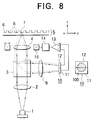
- Fig. 8 shows the configuration of a conventional tracking error detection device using a push-pull method, shown in Japanese Patent Kokoku Publication No. 1412/1992 and "G. Bouwhuis et al., Principles of Optical Disc System, Adam Hilger, pp.72 to 73 (1985)."
- reference numeral 1 denotes a light source such as a semiconductor laser, which emits a light beam for recording and reproduction.
- Reference numeral 2 denotes a collimator lens for converting the light beam from the light source 1 into a parallel beam.
- Reference numeral 3 denotes a beam splitter which passes the parallel beam from the collimator lens 2 and reflects the beam reflected at an information recording medium 5, which will be described later.
- Reference numeral 4 denotes an objective lens which focuses the light beam emitted from said light source 1 onto the information recording surface 6 of the information recording medium 5, such as an optical disk, and converts the beam reflected by the information recording medium 5 into a parallel beam.
- Reference numeral 7 denotes a light spot formed on the information recording surface 6 of the information recording medium 5.
- Reference numeral 8 denotes a track, which is parallel to the x direction, as shown in the figure. The y direction is perpendicular to the track 8 and is in a plane parallel to the information recording medium 5. The z direction is perpendicular to the information recording surface 6.
- Reference numeral 9 is a converging lens for concentrating a reflected beam in a suitable area on a split photodetector 10.
- the split photodetector has two light-receiving faces 11 and 12.
- Reference numeral 100 denotes a light spot on the split photodetector 10.
- the differential amplifier 13 produces a difference between the outputs from the light-receiving faces 11 and 12 as a tracking error signal TES.
- the tracking error signal TES is supplied via the phase-compensation circuit/amplifier 14 to the objective lens driving mechanism 15.
- the light spot 100 on the split photodetector 10 is circular as shown in Fig. 8.
- the split photodetector 10 is disposed so that the boundary between the light-receiving faces 11 and 12 divides the circular spot into upper and lower halves.
- the amount of light received by the light-receiving face 11 equals the amount of light received by the light-receiving face 12.
- the amount of light received at the light-receiving face 11 is different from the amount of light received at the light-receiving face 12.
- the direction (right or left) in which the light spot 7 deviates from the center of the track 8 determines whether the difference in amount of received light between the light-receiving faces 11 and 12 is positive or negative. Consequently, the difference in output between the light-receiving faces 11 and 12 can be treated as a tracking error signal.
- the lateral movement of the objective lens 4 to the position indicated by a dotted line causes the lateral movement of the light spot 100 to the position indicated by a dotted line on the split photodetector 10, as shown in Fig. 8. Consequently, the light-receiving faces 11 and 12 receive different amounts of amount of light even if the light spot 7 is at the center of the track 8.
- the light spot 100 on the split photodetector 10 deviates. Consequently, the light-receiving faces 11 and 12 receive different amounts of light even if the light spot 7 is at the center of the track 8.
- Japanese Patent Kokoku Publication No. 34212/1992 describes a method in which two light spots are disposed on an information recording medium, with a spacing of about a half of the track pitch; the beams returning from the two light spots are received by respective two split photodetectors; and the difference between the differential outputs of the two split photodetectors is treated as a tracking error signal.
- the configuration, operation, and problems of this method will next be described, with reference to Figs. 9 and 10.
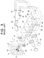
- Fig. 9 is a perspective view showing the configuration of another conventional tracking error detection device shown in Japanese Patent Kokoku Publication No. 34212/1992.
- reference numerals 16 and 17 denote light sources such as a semiconductor laser, from which light beams with different wavelengths are emitted (the oscillation wavelength from the light source 16 is represented by ⁇ 1 while the oscillation wavelength from the light source 17 is represented by ⁇ 2).
- Reference numerals 18 and 19 denote collimator lenses for converting light beams from the light sources 16 and 17 into parallel beams.
- Reference numeral 20 denotes a beam splitter which deflects the parallel beam with wavelength ⁇ 1 output from the collimator lens 18 by 90 degrees and directs the beam to the objective lens 4.
- Reference numeral 21 denotes another beam splitter which deflects the parallel beam with wavelength ⁇ 2 output from the collimator lens 19 by 90 degrees and directs the beam to the objective lens 4.
- the beam splitters 20 and 21 in combination serve to merge the light beams from the light sources 16 and 17.
- Reference numerals 22 and 23 denote light spots formed on the information recording surface 6 of the information recording medium 5.
- the light spot 22 is of the light beam having wavelength ⁇ 1 while the light spot 23 is of the light beam having wavelength ⁇ 2.
- the two light beams reflected by the information recording medium 5 are re-converted into parallel beams by the objective lens 4.
- the beams pass through the beam splitters 20 and 21, then reach the dichroic beam splitter 24.
- the dichroic beam splitter 24 passes the light beam with wavelength ⁇ 1 and reflects the light beam with wavelength ⁇ 2.
- the beam splitter 24 thus divides the light beams from the information recording medium 5 into the light beam having the wavelength ⁇ 1 and the light beam having the wavelength ⁇ 2.
- Reference numerals 25 and 28 denote split photodetectors, which have two light-receiving faces 26 and 27, and 29 and 30 respectively.
- the beam returning from the light spot 22 of the light beam with wavelength ⁇ 1 passes through the dichroic beam splitter 24 and reaches the split photodetector 25.
- the beam returning from the light spot 23 of the light beam with wavelength ⁇ 2 is reflected by the dichroic beam splitter 24 and reaches the split photodetector 28.
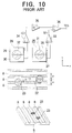
- Fig. 10 shows the relative positions of the light spots 22 and 23 on the information recording surface 6, the corresponding light spots on the split photodetectors 25 and 28, and a circuit for generating a tracking error signal.
- the figure shows that the information recording surface 6 of the information recording medium 5 has grooves and lands on it and that the tracks 8 are formed on the lands.
- the two light spots 22 and 23 are disposed with a spacing of p/2 in the y direction (direction perpendicular to the track), where p is the track pitch.
- Reference numerals 31 and 32 denote the light spots corresponding to the light spots 22 and 23 respectively on the split photodetectors.
- the outputs from the two light-receiving faces 26 and 27 of the single split photodetector 25 are input to the differential amplifier 33, from which differential output TE1 is obtained and supplied to the next differential amplifier 36.
- the outputs from the two light-receiving faces 29 and 30 of another split photodetector 28 are input to the differential amplifier 34, from which differential output TE2 is obtained.
- TE2 is supplied via the variable-gain amplifier 35 having gain G to the differential amplifier 36.
- the differential amplifier 36 outputs a difference between TE1 and TE2 multiplied by G, which is treated as tracking error signal TES.
- the tracking error signal TES is supplied via the phase-compensation circuit/amplifier 14 to the objective lens driving mechanism 15.
- the tracking error signal TES is free from the offset caused by the lateral movement of the objective lens.
- the offset results from the lateral movement of the spots on the split photodetector in the same direction caused by the lateral movement of the objective lens.
- the two spots 31 and 32 move in the y direction.
- the light-receiving faces 26 and 29 receive a greater amount of light than the light receiving faces 27 and 30.
- This causes a positive offset in TE1 and TE2, as indicated by a chain line in Fig. 11.
- the track crossing component generated by a light spot crossing the tracks 8 plotted on the time base varies in a sinusoidal fashion. Because the spacing between the light spots 22 and 23 in the y direction is just a half of the track pitch, the differential outputs TE1 and TE2 have opposite phases, as shown in Fig. 11.
- the offset can be eliminated from the tracking error signal TES, as shown in Fig. 11.
- the offset caused by a tilt of an information recording medium can be eliminated in the same way.
- the amplitude of the tracking error signal depends on the ratio of the spacing between the two light spots to the track pitch of the information recording medium.
- the dependence causes a problem especially when a single optical head is used to reproduce optical disks of different types with different track pitches. For example, let us assume that an optical head is adjusted to so that the spacing between the light spots on an optical disk of which track pitch is p is p/2, which is a half of the track pitch (so that the amplitude of the tracking error signal is maximized). When this optical head for a disk of which track pitch is about p/2 is used, the resultant amplitude of the tracking error signal will be almost zero. This is because, in this method, the amplitude of the tracking error signal is maximized when the spacing between two light spots is an odd multiple of a half of the track pitch, and the amplitude is zero when the spacing is an integral multiple of the track pitch.
- the invention has been made to solve the problems described above, and its object is to provide an optical head tracking error detection device which can reduce the offset caused by the lateral movement of the objective lens or a tilt of the information recording medium and can maintain the maximum amplitude of the tracking error signal, irrespective of variations in track pitch of the information recording medium.
- Another object of the invention is to simplify the configuration of an optical system of an optical head tracking error detection device.
- An optical head tracking error detection device comprises:
- the offset components included in the differential outputs of a pair of split photodetectors are in phase and the track crossing components have opposite phases. Consequently, the offset components can be eliminated from the tracking error signal, which is the difference of differential outputs obtained from the pair of split photodetectors.
- An optical head tracking error detection device comprises:
- the differential outputs of three split photodetectors include offset components which are all in phase.
- the track crossing components of the differential outputs obtained from two of the three split photodetectors are 180 degrees out of phase with the differential output of the remaining one split photodetectors. Consequently, the offset components can be eliminated from the tracking error signal obtained by adding and subtracting the differential outputs of three split photodetectors.
- the offset and the dependence of the detection sensitivity on the track pitch can be minimized, and the requirements of the positioning accuracy of the light spots and the accuracy of the phase difference of the phase difference addition means can be relaxed.
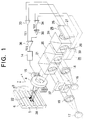
- Fig. 1 is a perspective view showing the configuration of an optical head tracking error detection device of Embodiment 1 of the invention.
- reference numerals 4 to 6, 8, 14 to 22, 24 to 30, and 33 to 36 denote members identical to those in Figs. 8 and 9 showing conventional tracking error detection devices.
- Reference numeral 37 denotes phase difference addition means for giving a phase difference of about 180 degrees between substantially-half portions of the light beam emitted from the light source 17.
- Reference numeral 38 denotes a light spot formed by the light beam emitted from the light source 17 on the information recording surface 6 of the information recording medium 5.
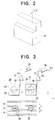
- Fig. 2 is a schematic representation of an example of the phase difference addition means included in Fig. 1.
- the phase difference addition means 37 is made of a plate of a transparent material having a refractive index of n and has two levels separated by a line running substantially through its center, at which the thickness changes by d.
- the incident light beam is divided at the linear part where the thickness changes.
- the upper half circle and the lower half circle are given a phase difference proportional to the thickness change d.
- d should be set so that (n - 1)d is a half of the wavelength ⁇ 2 of the light source 17.
- n equals 1.5 and ⁇ 2 equals 0.78 ⁇ m, for example, d should be 0.78 ⁇ m.
- Fig. 3 shows the relative positions of the light spots 22 and 38 on the information recording surface 6, light spots on the corresponding split photodetectors 25 and 28, and a circuit for generating a tracking error signal in Embodiment 1 of the invention.
- reference numerals 8, 22, and 25 to 36 denote members identical to those in Figs. 8 and 9, which show examples of prior art.
- the circuit for generating a tracking error signal is the same as the circuit of prior art shown in Fig. 10.
- the light spot 38 is not substantially circular but consists of two elliptical subspots, which results from a phase difference of about 180 degrees between substantially-half portions of the light beam from the light source 17; and the spacing in the y direction (direction perpendicular to the tracks) between the light spots 38 and 22 is zero.
- the spacing between the light spots 22 and 38 is defined by the distance in the lateral direction of the track between the center of the light spot 22 and the midpoint between the centers of the sub-spots forming the light spot 38.
- Fig. 3 shows two light spots disposed with no spacing in the y direction, however, in general terms the spacing may be an integral multiple of the track pitch. That is, the expression "an integral multiple of the track pitch" as used in the appended claims should be construed to include a situation where the spacing is zero.
- a(x, y) ⁇ (x, y) ⁇ exp ⁇ 2 ⁇ i ⁇ W(x, y) ⁇
- ⁇ (x, y) is the absolute value of the amplitude distribution of the directed light
- W(x, y) is the wavefront aberration.
- ⁇ (x, y) is assumed to be 1
- W(x, y) is assumed to be zero.
- Ad(x', y') ⁇ R n ⁇ exp ⁇ -2 ⁇ i ⁇ nv 0 /q ⁇ a(-x', -y' + n/q) It is assumed here that the optical disk is uniform in the x direction but has periodicity in the y direction (direction perpendicular to the tracks). v 0 is a normalized track deviation, and q is a normalized track pitch.
- Ad -1 R 0 + R -1 ⁇ exp ⁇ 2 ⁇ i ⁇ v 0 /q ⁇
- Ad 1 2 R 0 2 [(1 + ⁇ 1 2 ) + 2 ⁇ 1 ⁇ cos( ⁇ 1 - 2 ⁇ ⁇ v 0 /q)]
- Ad -1 2 R 0 2 [(1 + ⁇ -1 2 ) + 2 ⁇ -1 ⁇ cos( ⁇ -1 + 2 ⁇ ⁇ v 0 /q)]
- Id 1 and Id -1 K 1 ⁇ Ad 1 2 + I 0 /2
- Id -1 K -1 ⁇ Ad -1 2 + I 0 /2
- K 1 and K -1 are the products of the sensitivity of the light-receiving faces and the size of the areas A and B
- I 0 is an output current from the area hit just by the zeroth-order light in the vicinity of the origin shown in Fig. 4.
- the tracking error signal TES is given as a difference between Id 1 and Id -1 .
- Ad inv (x', y') ⁇ R n ⁇ exp ⁇ -2 ⁇ i ⁇ nv 0 /q) ⁇ a(-x', -y' + n/q)
- Ad 1inv R 0 ⁇ a(-x', -y') + R 1 ⁇ exp ⁇ -2 ⁇ i ⁇ v 0 /q ⁇ ⁇ a inv (-x', -y' + 1/q)
- a inv (-x', -y') in the equation given above can be calculated as follows: Since the value of 1/q of a normal optical disk is around 1, (-y' + 1/q) is positive in most cases. a inv (-x', -y' + 1/q) in the area A is therefore calculated as follows:
- Ad -1inv R 0 ⁇ a(-x', -y') + R -1 ⁇ exp ⁇ 2 ⁇ i ⁇ v 0 /q ⁇ ⁇ a inv (-x', -y' -1/q)
- a inv (-x', -y') in the equation given above can be calculated as follows: Since the value of 1/q of a normal optical disk is around 1, (-y' - 1/q) is negative in most cases. a inv (-x', -y'-1/q) of the area B is therefore calculated as follows:
- Ad 1inv exp(-i ⁇ /2) ⁇ R 0 [1 - ⁇ 1 ⁇ exp ⁇ i( ⁇ 1 - 2 ⁇ ⁇ v 0 /q) ⁇ ]
- Ad -1inv exp(i ⁇ /2) ⁇ R 0 [1 - ⁇ -1 ⁇ exp ⁇ i( ⁇ -1 + 2 ⁇ ⁇ v 0 /q) ⁇ ]
- Ad 1inv 2 R 0 2 [(1 + ⁇ 1 2 ) - 2 ⁇ 1 ⁇ cos( ⁇ 1 - 2 ⁇ v 0 /q)]
- Ad -1inv 2 R 0 2 [(1 + ⁇ -1 2 ) - 2 ⁇ -1 ⁇ cos( ⁇ -1 + 2 ⁇ v 0 /q)]
- Id 1inv K 1 ⁇ Ad 1inv 2 + I 0 /2
- Id -1inv K -1 ⁇ Ad -1inv 2 + I 0 /2
- the tracking error signal TE inv is given as a difference between Id 1inv and Id -1inv .
- TE inv K 1 R 0 2 ⁇ 4 ⁇ 1 sin ⁇ 1 ⁇ [-sin(2 ⁇ v 0 /q)]
- the expression of TE inv is the same as the expression of TE, except the signs are inverted. This indicates that TE inv and TE have opposite phases about the track deviation, but otherwise they are equal.
- the offset component occurs when the light spot 31 on the photodetector 25 moves in the positive y direction.
- Al is the amplitude of the track crossing component.
- B2 ⁇ u is the offset component proportional to u when u is small.
- the offset component occurs when the light spot 32 on the photodetector 28 moves in the positive y direction. (This indicates that the lateral movement of an objective lens causes the spots 31 and 32 to move in the same direction.
- the coefficient B2 has the same sign as the coefficient B1.)
- the track crossing component of TE2 is 180 degrees out of phase with TE1, and -A2 is the amplitude of the track crossing component (the coefficient A2 has the same sign as the coefficient Al).
- the gain G of a variable-gain amplifier equals the ratio of B1 to B2
- the following tracking error signal TES is obtained: This indicates that the offset component can be eliminated from the tracking error signal TES.
- the amplitude of the tracking error signal depends on the ratio of the spacing between two light spots to the track pitch of the information recording medium.
- the tracking error detection device of Embodiment 1 however, two light spots are disposed parallel with tracks, as shown in Fig. 3. Consequently, a problem which arises when a single optical head reproduces optical disks of different types with different track pitches can be solved, and the amplitude of the tracking error signal will not be almost zero with any track pitch. This is because two light spots are parallel with tracks, irrespective of the track pitch.
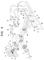
- Fig. 5 is a perspective view showing the configuration of a tracking error detection device of Embodiment 2 of the invention.
- reference numerals 1, 2, 4, 5, 6, 8, 9, 14, and 15 denote members identical to those conventional tracking error detection devices shown in Figs. 8 and 9.
- Reference numeral 39 denotes a diffraction grating which divides a light beam from the light source 1 into three light beams and functions as phase difference addition means for giving a phase difference of about 180 degrees between substantially-half portions of each of two of the three light beams.
- Reference numeral 40 denotes a beam splitter which reflects the parallel beams from the collimator lens 2 and passes the beam reflected by the information recording medium 5.
- Reference numerals 41, 42, and 43 are three light spots formed on the information recording surface 6.
- the beams returning from the three light spots 41, 42, and 43 are passed through a converging lens 54 and received by three split photodetectors 25, 28, and 45 incorporated in a single package.
- the split photodetector 45 is an addition to Embodiment 1, and it has two light-receiving faces 46 and 47. As shown in Fig. 7, which will be described later, the light spots 48, 49, and 50 are formed on the three split photodetectors 25, 28, and 45 respectively.
- Reference numeral 51 denotes a differential amplifier to which the outputs of the split photodetector 45 are supplied.
- Reference numerals 52 and 53 denote variable-gain amplifiers of which gains are G1 and G2 respectively.
- Fig. 6 is a schematic representation of the structure of the diffraction grating 39, which is provided as phase difference addition means in Embodiment 2 of the invention.
- the grating 39 is generally made of a plate of an optical glass or other transparent material having the first and second sections, each provided with an array of linear concaves and convexes adjacent to each other, which are formed by photolithographic etching, or other process.
- the period of the diffraction grating is set between 10 and 100 ⁇ m.
- the periodic structures of the upper and lower haves or sections are 180 degrees out of phase. It will next be described whether the diffraction grating 39 can generate a phase difference of 180 degrees between the upper and lower halves of the first-order and minus-first-order diffracted beams.
- u 1 (x 1 ) h(x 1 ) (when y 1 > 0: upper half)
- ⁇ is the period of the diffraction grating.
- u 2a (x 2 ) k ⁇ (x 1 ) ⁇ exp(i ⁇ 2 ⁇ x 1 x 2 / ⁇ L)dx 1 where ⁇ is the wavelength of the light beam and L is the propagation distance.
- Fig. 7 shows the relative positions of the three light spots 41, 42, and 43 on the information recording surface 6, light spots on the corresponding split photodetectors 25, 28 and 45, and a circuit for generating a tracking error signal in Embodiment 2 of the invention.
- reference numeral 41 denotes a light spot by the zeroth-order diffracted light
- 42 denotes a light spot by the minus-first-order diffracted light
- 43 denotes a light spot by the first-order diffracted light.
- the circuit for generating a tracking error signal TES is similar to the corresponding circuit of Embodiment 1 shown in Fig.
- the differential amplifier 51 which outputs the difference between the outputs of the split photodetector 45 and the variable-gain amplifier 53 with gain G2 which receives the differential output TE3 of the differential amplifier 51 are added; and the variable-gain amplifier 35 with gain G in Fig. 3 is replaced by the variable-gain amplifier 52 with gain G1.
- the differential output TE1, differential output TE2 multiplied by G1, and differential output TE3 multiplied by G2 are supplied to the differential amplifier 36, which outputs the tracking error signal TES.
- the light spot 41 is substantially circular, as is usual, and the light spots 42 and 43 consist of two elliptical subspots.
- the diffraction grating 39 is rotated for adjustment so that the spacing in the y-direction (direction perpendicular to the tracks) between two adjacent spots of the light spots 41, 42, and 43 is substantially zero.
- the spacing between the adjacent light spots e.g., 41 and 42, is defined by the distance in the lateral direction of the track between the center of the light spot 41 and the midpoint between the centers of the sub-spots forming the light spot 42.
- the spacing between adjacent light spots is zero.
- the spacing may be an integral multiple of the track pitch. That is, the expression "an integral multiple of the track pitch" as used in the appended claims should be construed to include a situation where the spacing is zero.
- the offset components can be eliminated from the tracking error signal TES in Embodiment 2 as well.
- the principle of the elimination of the offset components is the same as that in Embodiment 1.
- the offset can be theoretically zero even if the y-direction spacing between adjacent light spots is not just zero.
- the offset component occurs when the light spot 48 on the photodetector 25 moves in the positive y direction.
- Al is the amplitude of the track crossing component.
- B2 ⁇ u is the offset component proportional to u when u is small.
- the offset component occurs when the light spot 49 on the photodetector 28 moves in the positive y direction.
- the track crossing component of TE2 is 180 x (1 + e/q) degrees out of phase with TE2 and has the amplitude - A2. (The coefficient A2 has the same sign as the coefficient A1.)
- the offset component occurs when the light spot 50 on the photodetector 45 moves in the positive y direction.
- the track crossing component of TE3 is 180 x (1 - e/q) degrees out of phase with TE1 and has the amplitude - A3.
- the coefficient A3 has the same sign as the coefficient A1.
- the gains G1 and G2 of the variable-gain amplifiers 52 and 53 are so set that the ratio G2/G1 between the gains G1 and G2 equals the ratio A2/A3 between the amplitude A2 of the track crossing component of the differential output TE2 and the amplitude A3 of the track crossing component of differential output TE3, the addition yields the following:
- the amplitude of the tracking error signal TES varies with the magnitude of e and is maximized when the value of e/q is an integer, that is, when the y-direction spacing between adjacent light spots is just an integral multiple of the track pitch.
- phase difference between the periodic structures of the upper and lower halves of the diffraction grating deviates from 180 degrees, which is normally expected, by 180 ⁇ ⁇ / ⁇ ( ⁇ radians) in Embodiment 2.
- the phase difference between the upper and lower halves of the plus/minus-first-order diffracted light should be found.
- TE2 is a signal obtained from the first-order diffracted light generated by the diffraction grating 39. Adding a phase difference of ( ⁇ + ⁇ ) radians to the first-order diffracted light is equivalent to adding ⁇ /(4 ⁇ ) to 0.25 in the equation (15).
- TE3 is a signal obtained from the minus-first-order diffracted light generated by the diffraction grating 39. Adding a phase difference of -( ⁇ + ⁇ ) radians to the phase difference between the upper and lower halves is equivalent to using the equation (50) instead of the equation (15).
- W inv (x, y) -0.25 - ⁇ /(4 ⁇ ) (when y > 0)
- W inv (x, y) 0.25 + ⁇ /(4 ⁇ ) (when y ⁇ 0)
- the gains G1 and G2 of the variable-gain amplifiers 52 and 53 are so set that the ratio G2/G1 between the gains G1 and G2 equals the ratio A2/A3 between the amplitude A2 of the track crossing component of the differential output TE2 and the amplitude A3 of the track crossing component of differential output TE3, the addition yields the signal TE' having a track crossing component proportional to -cos ⁇ ⁇ sin(2 ⁇ v 0 /q). Regardless of the ⁇ value, no offset occurs in the signal TE'. The amplitude of the signal TE', however, decreases in proportion to the cosine of ⁇ . Since TE1 is originally not related to ⁇ , the tracking error signal TES, which is obtained from the difference between TE' and TE1 multiplied by G1, has no offset.
- Embodiment 2 includes the advantages of Embodiment 1 described earlier and the relaxed requirements of the positioning accuracy of the light spots on the information recording medium and the accuracy of the phase difference given by the phase difference addition means.
Landscapes
- Physics & Mathematics (AREA)
- Optics & Photonics (AREA)
- Optical Recording Or Reproduction (AREA)
- Optical Head (AREA)
Abstract
Description
- The present invention relates to a device for detecting a tracking error of an optical head for optically recording and reproducing information, and particularly a tracking error detection device which produces little offset and in which the detection sensitivity has little dependence on the tracking pitch.
- Fig. 8 shows the configuration of a conventional tracking error detection device using a push-pull method, shown in Japanese Patent Kokoku Publication No. 1412/1992 and "G. Bouwhuis et al., Principles of Optical Disc System, Adam Hilger, pp.72 to 73 (1985)." In the figure,
reference numeral 1 denotes a light source such as a semiconductor laser, which emits a light beam for recording and reproduction.Reference numeral 2 denotes a collimator lens for converting the light beam from thelight source 1 into a parallel beam.Reference numeral 3 denotes a beam splitter which passes the parallel beam from thecollimator lens 2 and reflects the beam reflected at aninformation recording medium 5, which will be described later.Reference numeral 4 denotes an objective lens which focuses the light beam emitted fromsaid light source 1 onto theinformation recording surface 6 of theinformation recording medium 5, such as an optical disk, and converts the beam reflected by the information recordingmedium 5 into a parallel beam.Reference numeral 7 denotes a light spot formed on theinformation recording surface 6 of theinformation recording medium 5.Reference numeral 8 denotes a track, which is parallel to the x direction, as shown in the figure. The y direction is perpendicular to thetrack 8 and is in a plane parallel to the information recordingmedium 5. The z direction is perpendicular to theinformation recording surface 6.Reference numeral 9 is a converging lens for concentrating a reflected beam in a suitable area on asplit photodetector 10. The split photodetector has two light-receiving faces Reference numeral 100 denotes a light spot on thesplit photodetector 10. Thedifferential amplifier 13 produces a difference between the outputs from the light-receivingfaces amplifier 14 to the objectivelens driving mechanism 15. - The operation of the conventional tracking error detection device shown in Fig. 8 will next be described. The
light spot 100 on thesplit photodetector 10 is circular as shown in Fig. 8. Thesplit photodetector 10 is disposed so that the boundary between the light-receivingfaces light spot 7 travels along thetrack 8 at its center, the amount of light received by the light-receivingface 11 equals the amount of light received by the light-receivingface 12. When thelight spot 7 deviates from the center of thetrack 8, the amount of light received at the light-receivingface 11 is different from the amount of light received at the light-receivingface 12. The direction (right or left) in which thelight spot 7 deviates from the center of thetrack 8 determines whether the difference in amount of received light between the light-receivingfaces faces - The lateral movement of the
objective lens 4 to the position indicated by a dotted line causes the lateral movement of thelight spot 100 to the position indicated by a dotted line on thesplit photodetector 10, as shown in Fig. 8. Consequently, the light-receivingfaces light spot 7 is at the center of thetrack 8. - When the
information recording medium 5 tilts relative to the y direction, thelight spot 100 on thesplit photodetector 10 deviates. Consequently, the light-receivingfaces light spot 7 is at the center of thetrack 8. - As a solution to these problems, Japanese Patent Kokoku Publication No. 34212/1992 describes a method in which two light spots are disposed on an information recording medium, with a spacing of about a half of the track pitch; the beams returning from the two light spots are received by respective two split photodetectors; and the difference between the differential outputs of the two split photodetectors is treated as a tracking error signal. The configuration, operation, and problems of this method will next be described, with reference to Figs. 9 and 10.
- Fig. 9 is a perspective view showing the configuration of another conventional tracking error detection device shown in Japanese Patent Kokoku Publication No. 34212/1992. In the figure,
reference numerals light source 16 is represented byλ 1 while the oscillation wavelength from thelight source 17 is represented by λ 2).Reference numerals light sources Reference numeral 20 denotes a beam splitter which deflects the parallel beam withwavelength λ 1 output from thecollimator lens 18 by 90 degrees and directs the beam to theobjective lens 4.Reference numeral 21 denotes another beam splitter which deflects the parallel beam withwavelength λ 2 output from thecollimator lens 19 by 90 degrees and directs the beam to theobjective lens 4. Thebeam splitters light sources Reference numerals information recording surface 6 of theinformation recording medium 5. Thelight spot 22 is of the light beam havingwavelength λ 1 while thelight spot 23 is of the light beam havingwavelength λ 2. - The two light beams reflected by the
information recording medium 5 are re-converted into parallel beams by theobjective lens 4. The beams pass through thebeam splitters dichroic beam splitter 24. Thedichroic beam splitter 24 passes the light beam withwavelength λ 1 and reflects the light beam withwavelength λ 2. Thebeam splitter 24 thus divides the light beams from the information recordingmedium 5 into the light beam having thewavelength λ 1 and the light beam having thewavelength λ 2.Reference numerals faces light spot 22 of the light beam withwavelength λ 1 passes through thedichroic beam splitter 24 and reaches thesplit photodetector 25. The beam returning from thelight spot 23 of the light beam withwavelength λ 2 is reflected by thedichroic beam splitter 24 and reaches thesplit photodetector 28. - Fig. 10 shows the relative positions of the
light spots information recording surface 6, the corresponding light spots on thesplit photodetectors information recording surface 6 of theinformation recording medium 5 has grooves and lands on it and that thetracks 8 are formed on the lands. The twolight spots Reference numerals light spots receiving faces single split photodetector 25 are input to thedifferential amplifier 33, from which differential output TE1 is obtained and supplied to the nextdifferential amplifier 36. The outputs from the two light-receiving faces split photodetector 28 are input to thedifferential amplifier 34, from which differential output TE2 is obtained. TE2 is supplied via the variable-gain amplifier 35 having gain G to thedifferential amplifier 36. Thedifferential amplifier 36 outputs a difference between TE1 and TE2 multiplied by G, which is treated as tracking error signal TES. The tracking error signal TES is supplied via the phase-compensation circuit/amplifier 14 to the objectivelens driving mechanism 15. - Next, it will be briefly described that the tracking error signal TES is free from the offset caused by the lateral movement of the objective lens. As described above, the offset results from the lateral movement of the spots on the split photodetector in the same direction caused by the lateral movement of the objective lens. In Fig. 10, the two
spots faces faces tracks 8 plotted on the time base varies in a sinusoidal fashion. Because the spacing between thelight spots - When the gain G of the variable-
gain amplifier 35 is adjusted to the ratio of the offset of the differential output TE1 to the offset of the differential output TE2, the offset can be eliminated from the tracking error signal TES, as shown in Fig. 11. The offset caused by a tilt of an information recording medium can be eliminated in the same way. - Since the latter conventional tracking error detection device is configured as described above, the amplitude of the tracking error signal depends on the ratio of the spacing between the two light spots to the track pitch of the information recording medium. The dependence causes a problem especially when a single optical head is used to reproduce optical disks of different types with different track pitches. For example, let us assume that an optical head is adjusted to so that the spacing between the light spots on an optical disk of which track pitch is p is p/2, which is a half of the track pitch (so that the amplitude of the tracking error signal is maximized). When this optical head for a disk of which track pitch is about p/2 is used, the resultant amplitude of the tracking error signal will be almost zero. This is because, in this method, the amplitude of the tracking error signal is maximized when the spacing between two light spots is an odd multiple of a half of the track pitch, and the amplitude is zero when the spacing is an integral multiple of the track pitch.
- The invention has been made to solve the problems described above, and its object is to provide an optical head tracking error detection device which can reduce the offset caused by the lateral movement of the objective lens or a tilt of the information recording medium and can maintain the maximum amplitude of the tracking error signal, irrespective of variations in track pitch of the information recording medium.
- Another object of the invention is to simplify the configuration of an optical system of an optical head tracking error detection device.
- An optical head tracking error detection device according to a first aspect of the invention comprises:
- means for directing and focusing two light beams onto an information recording medium to form first and second light spots;
- first and second split photodetectors for respectively receiving the light beams returning from the respective light spots on said information recording medium, each of said split photo detectors having a pair of light receiving faces, and each of the light receiving faces receiving a substantially equal portion of the returning light if the light spots are just focused on the information recording medium and are tracking correctly;
- means for producing a tracking error signal on the basis of the difference between differential outputs of said first and second split photodetectors; and
- phase difference addition means for introducing a phase difference of substantially 180 degrees between substantially-half portions of one of said two beams directed to said information recording medium;
- said directing and focusing means disposes said light spots on said information recording medium such that a spacing between the light spots in the direction perpendicular to tracks on said information recording medium is substantially an integral multiple of track pitch.
- According to the above optical head tracking error detection device, the offset components included in the differential outputs of a pair of split photodetectors are in phase and the track crossing components have opposite phases. Consequently, the offset components can be eliminated from the tracking error signal, which is the difference of differential outputs obtained from the pair of split photodetectors.
- Accordingly, the offset and the dependence of the detection sensitivity on the track pitch can be minimized.
- An optical head tracking error detection device according to a second aspect of the invention comprises:
- means for directing and focusing three light beams onto an information recording medium to form first, second and third light spots on said information recording medium;
- first, second and third split photodetectors for respectively receiving the light beams returning from the first, second and third light spots on said information recording medium, each of said split photo detectors having a pair of light receiving faces, and each of the light receiving faces receives a substantially equal portion of the returning light if the light spots are just focused on the information recording medium and are tracking correctly; and
- means for producing a tracking error signal on the basis of differential outputs of said first, second and third split photodetectors;
- wherein said directing and focusing means comprises a diffraction grating consisting of first and second sections respectively having periodic structures which are out of phase by about 180 degrees, for giving a phase difference of substantially 180 degrees to substantially-half portions of the two of the three beams; and disposes said light spots on said information recording medium such that a spacing between two adjacent light spots in the direction perpendicular to tracks on said information recording medium is substantially an integral multiple of track pitch.
- According to the above optical head tracking error detection device, the differential outputs of three split photodetectors include offset components which are all in phase. The track crossing components of the differential outputs obtained from two of the three split photodetectors are 180 degrees out of phase with the differential output of the remaining one split photodetectors. Consequently, the offset components can be eliminated from the tracking error signal obtained by adding and subtracting the differential outputs of three split photodetectors.
- Accordingly, the offset and the dependence of the detection sensitivity on the track pitch can be minimized, and the requirements of the positioning accuracy of the light spots and the accuracy of the phase difference of the phase difference addition means can be relaxed.
- In the accompanying drawings:-
- Fig. 1 is a perspective view showing the configuration of an optical head tracking error detection device in
Embodiment 1 of the invention; - Fig. 2 is a schematic representation of an example of the phase difference addition means included in Fig. 1;
- Fig. 3 shows the relative positions of light spots on an information recording surface, split photodetectors, and a circuit for generating a tracking error signal in
Embodiment 1 of the invention; - Fig. 4 shows the light reflected by the optical disk in
Embodiment 1 of the invention; - Fig. 5 is a perspective view showing the configuration of an optical head tracking error detection device in
Embodiment 2 of the invention; - Fig. 6 is a schematic representation of the structure of a diffraction grating provided as phase difference addition means in
Embodiment 2 of the invention; - Fig. 7 shows the relative positions of light spots on an information recording surface, split photodetectors, and a circuit for generating a tracking error signal in
Embodiment 2 of the invention; - Fig. 8 is a schematic representation of the configuration of a conventional tracking error detection device;
- Fig. 9 is a perspective view showing the configuration of another conventional tracking error detection device;
- Fig. 10 shows the relative positions of light spots on an information recording surface, split photodetectors, and a circuit for generating a tracking error signal in another conventional tracking error detection device; and
- Fig. 11 shows the differential outputs of split photodetectors and tracking error signals in another conventional tracking error detection device.
- This invention will be described in detail with reference to the drawings showing embodiments of the invention.
- Fig. 1 is a perspective view showing the configuration of an optical head tracking error detection device of
Embodiment 1 of the invention. In the figure,reference numerals 4 to 6, 8, 14 to 22, 24 to 30, and 33 to 36 denote members identical to those in Figs. 8 and 9 showing conventional tracking error detection devices.Reference numeral 37 denotes phase difference addition means for giving a phase difference of about 180 degrees between substantially-half portions of the light beam emitted from thelight source 17.Reference numeral 38 denotes a light spot formed by the light beam emitted from thelight source 17 on theinformation recording surface 6 of theinformation recording medium 5. - Fig. 2 is a schematic representation of an example of the phase difference addition means included in Fig. 1. The phase difference addition means 37 is made of a plate of a transparent material having a refractive index of n and has two levels separated by a line running substantially through its center, at which the thickness changes by d. The incident light beam is divided at the linear part where the thickness changes. The upper half circle and the lower half circle are given a phase difference proportional to the thickness change d. To make the phase difference equal to 180 degrees, d should be set so that (n - 1)d is a half of the
wavelength λ 2 of thelight source 17. When n equals 1.5 andλ 2 equals 0.78 µm, for example, d should be 0.78 µm. - Fig. 3 shows the relative positions of the light spots 22 and 38 on the
information recording surface 6, light spots on thecorresponding split photodetectors Embodiment 1 of the invention. In the figure,reference numerals light spot 38 is not substantially circular but consists of two elliptical subspots, which results from a phase difference of about 180 degrees between substantially-half portions of the light beam from thelight source 17; and the spacing in the y direction (direction perpendicular to the tracks) between thelight spots light spots light spot 22 and the midpoint between the centers of the sub-spots forming thelight spot 38. Fig. 3 shows two light spots disposed with no spacing in the y direction, however, in general terms the spacing may be an integral multiple of the track pitch. That is, the expression "an integral multiple of the track pitch" as used in the appended claims should be construed to include a situation where the spacing is zero. - The principle of generation of a tracking error signal in the push-pull method, which will be needed to describe the operation of
Embodiment 1, will next be described, based on Hopkins' theory. The complex amplitude distribution of the directed light on the exit pupil of an objective lens, represented by a(x, y), can be generally expressed as follows:

- The complex amplitude distribution of reflected light in the area A (see Fig. 4) where the zeroth-order reflected light overlaps the reflected light subjected to the first-order (n = 1) diffraction caused by the periodicity of the optical disk, represented by Ad1, given by the following equation:

- The complex amplitude distribution of reflected light in the area B (see Fig. 4) where the zeroth-order reflected light overlaps the reflected light subjected to the minus-first-order (n = -1) diffraction caused by the periodicity of the optical disk, represented by Ad-1, is given by the following equation:

- Substituting R1 and R-1 that can be expressed as follows:


- The light intensity distributions in the areas A and B are given by the square of the equations (7) and (8) respectively, as shown below:


- When the two light-receiving faces of a split photodetector are disposed in a half area of Y' > 0 including the area A, and in another half area of y' < 0 including the area B, the outputs from the two light-receiving faces, represented by Id1 and Id-1, are given by the following equations:


- If two light-receiving faces are equal in sensitivity and size and if an optical disk has such a periodic structure that is symmetric about a plane perpendicular to the surface of the disk and passing the center line of the track, (strictly, passing a line tangential to the center line of the track), these equations are satisfied:


- The principle of generating a tracking error signal in the push-pull method from a beam having halves 180 degrees out of phase, which is characteristic to
Embodiment 1 will next be described, based on Hopkins's theory. The complex amplitude distribution of the directed light on the exit pupil of an objective lens, represented by ainv(x, y), can be expressed as follows:

- The complex amplitude distribution of the light reflected by a disk on a photodetector, represented by Adinv(x', y'), is given by the following expression:

- The complex amplitude distribution of reflected light in the area A where the zeroth-order reflected light overlaps the reflected light subjected to the first-order (n = 1) diffraction caused by the periodicity of the optical disk, represented by Ad1inv, satisfies the following equation:

- Since the area A is normally in an area of y' > 0, ainv(-x', -y') in the equation given above can be calculated as follows:


- Substituting the equations (18) and (19) into the equation (17) yields the following:

- The complex amplitude distribution of reflected light in the area B where the zeroth-order reflected light overlaps the reflected light subjected to the minus-first-order (n = -1) diffraction caused by the periodicity of the optical disk, represented by Ad-1inv, is given by the following equation:

- Since the area B is normally in an area of y' < 0, ainv(-x', -y') in the equation given above can be calculated as follows:


- Substituting the equations (22) and (23) into the equation (21) yields the following:

- Substituting the expressions (5) and (6) in the equations (23) and (24) yields the following:


- The light intensity distributions in the areas A and B are given by the square of the equations (25) and (26) respectively, as shown below:


- The outputs from the two light-receiving faces, represented by Id1inv and Id-1inv, satisfy the following equations:


- The tracking error signal TEinv is given as a difference between Id1inv and Id-1inv.

- With reference to Fig. 3, it will be described next that almost all offset components caused by the lateral movement of the objective lens and other reasons are eliminated from the tracking error signal TES obtained in
Embodiment 1. When the amount of lateral movement of the objective lens is u, the differential output TE1 obtained in the usual push-pull method can be expressed by the use of the equation (13), as follows:
light spot 31 on thephotodetector 25 moves in the positive y direction. Al is the amplitude of the track crossing component. The differential output TE2 in the push-pull method obtained from a beam having halves 180 degrees out of phase under the same condition can be given by the equation (31), as shown below:
light spot 32 on thephotodetector 28 moves in the positive y direction. (This indicates that the lateral movement of an objective lens causes thespots - As described above, the track crossing component of TE2 is 180 degrees out of phase with TE1, and -A2 is the amplitude of the track crossing component (the coefficient A2 has the same sign as the coefficient Al). When the gain G of a variable-gain amplifier equals the ratio of B1 to B2, the following tracking error signal TES is obtained:

- It is clear that, when an optical disk tilts, the light spots 31 and 32 moves in the same direction on the photodetector. Consequently, the offset component can be eliminated from the tracking error signal TES.
- In the conventional tracking error detection devices, the amplitude of the tracking error signal depends on the ratio of the spacing between two light spots to the track pitch of the information recording medium. In the tracking error detection device of
Embodiment 1, however, two light spots are disposed parallel with tracks, as shown in Fig. 3. Consequently, a problem which arises when a single optical head reproduces optical disks of different types with different track pitches can be solved, and the amplitude of the tracking error signal will not be almost zero with any track pitch. This is because two light spots are parallel with tracks, irrespective of the track pitch. - Fig. 5 is a perspective view showing the configuration of a tracking error detection device of
Embodiment 2 of the invention. In the figure,reference numerals Reference numeral 39 denotes a diffraction grating which divides a light beam from thelight source 1 into three light beams and functions as phase difference addition means for giving a phase difference of about 180 degrees between substantially-half portions of each of two of the three light beams.Reference numeral 40 denotes a beam splitter which reflects the parallel beams from thecollimator lens 2 and passes the beam reflected by theinformation recording medium 5.Reference numerals information recording surface 6. The beams returning from the threelight spots lens 54 and received by threesplit photodetectors split photodetector 45 is an addition toEmbodiment 1, and it has two light-receiving faces 46 and 47. As shown in Fig. 7, which will be described later, the light spots 48, 49, and 50 are formed on the threesplit photodetectors Reference numeral 51 denotes a differential amplifier to which the outputs of thesplit photodetector 45 are supplied.Reference numerals - Fig. 6 is a schematic representation of the structure of the
diffraction grating 39, which is provided as phase difference addition means inEmbodiment 2 of the invention. The grating 39 is generally made of a plate of an optical glass or other transparent material having the first and second sections, each provided with an array of linear concaves and convexes adjacent to each other, which are formed by photolithographic etching, or other process. In an ordinary optical head, the period of the diffraction grating is set between 10 and 100 µm. As is clear from the figure, the periodic structures of the upper and lower haves or sections are 180 degrees out of phase. It will next be described whether thediffraction grating 39 can generate a phase difference of 180 degrees between the upper and lower halves of the first-order and minus-first-order diffracted beams. - When uniform light beams are directed to a diffraction grating, the amplitude distribution of the light immediately after the diffraction grating, represented by u1(x1), is given by the following:

- The relationship between the diffracted lights of the upper and lower halves will next be found by using the formula of Fraunhofer diffraction. The complex amplitude distribution of diffracted light from the area of y1 > 0, represented by u2a(x2), is given by the following equation:

- The complex amplitude distribution of diffracted light from the area of y1 < 0, represented by u2b(x2), is given by the following equation:


- When the light beam propagates by L, the x2 coordinate of the position of the plus/minus-first-order diffracted light is ±L·( λ / Λ ). Substituting ±L·( λ / Λ ) for x2 in the expression given above yields the following:

- Fig. 7 shows the relative positions of the three
light spots information recording surface 6, light spots on thecorresponding split photodetectors Embodiment 2 of the invention. In the figure,reference numeral 41 denotes a light spot by the zeroth-order diffracted light, 42 denotes a light spot by the minus-first-order diffracted light, and 43 denotes a light spot by the first-order diffracted light. The circuit for generating a tracking error signal TES is similar to the corresponding circuit ofEmbodiment 1 shown in Fig. 3, but thedifferential amplifier 51 which outputs the difference between the outputs of thesplit photodetector 45 and the variable-gain amplifier 53 with gain G2 which receives the differential output TE3 of thedifferential amplifier 51 are added; and the variable-gain amplifier 35 with gain G in Fig. 3 is replaced by the variable-gain amplifier 52 with gain G1. The differential output TE1, differential output TE2 multiplied by G1, and differential output TE3 multiplied by G2 are supplied to thedifferential amplifier 36, which outputs the tracking error signal TES. Of the threelight spots information recording surface 6, thelight spot 41 is substantially circular, as is usual, and the light spots 42 and 43 consist of two elliptical subspots. Thediffraction grating 39 is rotated for adjustment so that the spacing in the y-direction (direction perpendicular to the tracks) between two adjacent spots of the light spots 41, 42, and 43 is substantially zero. Here, the spacing between the adjacent light spots, e.g., 41 and 42, is defined by the distance in the lateral direction of the track between the center of thelight spot 41 and the midpoint between the centers of the sub-spots forming thelight spot 42. In Fig. 7, the spacing between adjacent light spots is zero. However, in general terms the spacing may be an integral multiple of the track pitch. That is, the expression "an integral multiple of the track pitch" as used in the appended claims should be construed to include a situation where the spacing is zero. - It will be described next that the offset components can be eliminated from the tracking error signal TES in
Embodiment 2 as well. The principle of the elimination of the offset components is the same as that inEmbodiment 1. InEmbodiment 2, however, the offset can be theoretically zero even if the y-direction spacing between adjacent light spots is not just zero. When the amount of lateral movement of the objective lens is u, the differential output TE1 obtained in the usual push-pull method can be expressed as follows by using the equation (13), as in Embodiment 1:
light spot 48 on thephotodetector 25 moves in the positive y direction. Al is the amplitude of the track crossing component. - The differential output TE2 in the push-pull method obtained from a beam having halves 180 degrees out of phase under the same condition can be given by using the equation (31), as follows:

light spots - B2·u is the offset component proportional to u when u is small. The offset component occurs when the
light spot 49 on thephotodetector 28 moves in the positive y direction. The track crossing component of TE2 is 180 x (1 + e/q) degrees out of phase with TE2 and has the amplitude - A2. (The coefficient A2 has the same sign as the coefficient A1.) The differential output TE3 in the push-pull method obtained from another beam having halves 180 degrees out of phase can be given by the equation (31), as follows:
light spot 50 on thephotodetector 45 moves in the positive y direction. The track crossing component of TE3 is 180 x (1 - e/q) degrees out of phase with TE1 and has the amplitude - A3. (The coefficient A3 has the same sign as the coefficient A1.) When the gains G1 and G2 of the variable-gain amplifiers 

- The gains G1 and G2 of the variable-
gain amplifiers 
- It will be described next what occurs if the phase difference between the periodic structures of the upper and lower halves of the diffraction grating deviates from 180 degrees, which is normally expected, by 180· δ/π ( δ radians) in
Embodiment 2. First, the phase difference between the upper and lower halves of the plus/minus-first-order diffracted light should be found. This corresponds to a case in which the following is substituted in the equation (35):


- TE2 will be determined next. TE2 is a signal obtained from the first-order diffracted light generated by the
diffraction grating 39. Adding a phase difference of (π + δ ) radians to the first-order diffracted light is equivalent to adding δ /(4 π ) to 0.25 in the equation (15). This yields the following:

- TE3 will then be determined. TE3 is a signal obtained from the minus-first-order diffracted light generated by the
diffraction grating 39. Adding a phase difference of -(π + δ ) radians to the phase difference between the upper and lower halves is equivalent to using the equation (50) instead of the equation (15).
- By calculating the equations (16) to (31) beginning with the equation (50), the track crossing component TE3t in TE3 can be obtained as follows:

- Consequently, when the gains G1 and G2 of the variable-
gain amplifiers - The advantages of
Embodiment 2 include the advantages ofEmbodiment 1 described earlier and the relaxed requirements of the positioning accuracy of the light spots on the information recording medium and the accuracy of the phase difference given by the phase difference addition means.
Claims (12)
- An optical head tracking error detection device comprising:means (16, 17, 18, 19, 20, 21) for directing and focusing two light beams onto an information recording medium to form first and second light spots;first and second split photodetectors (25, 28) for respectively receiving the light beams returning from the respective light spots on said information recording medium, each of said split photo detectors having a pair of light receiving faces, and each of the light receiving faces receiving a substantially equal portion of the returning light if the light spots are just focused on the information recording medium and are tracking correctly;means (33, 34, 35, 36) for producing a tracking error signal (TES) on the basis of the difference between differential outputs of said first and second split photodetectors; andphase difference addition means (37) for introducing a phase difference of substantially 180 degrees between substantially-half portions of one of said two beams directed to said information recording medium;said directing and focusing means disposes said light spots on said information recording medium such that a spacing between the light spots in the direction perpendicular to tracks on said information recording medium is substantially an integral multiple of track pitch.
- The optical head tracking error detection device according to claim 1, wherein said first light spot consists of a round spot, and said second light spots consists of a pair of elliptical sub-spots.
- The optical head tracking error detection device according to claim 1, wherein said directing and focusing means comprises:a first light source (16) for emitting a light beam of a first wavelength (λ1);a second light source (17) for emitting a light beam of a second wavelength (λ2) different from said first wavelength (λ1); andmeans (20, 21) for merging the first and second light beams; andsaid phase difference addition means (37) is interposed in the optical path between said second light source (17) and said merging means (20, 21).
- The optical head tracking error detection device according to claim 3, wherein said phase difference addition means (37) comprises a plate of transparent material having a stepwise change in the thickness along a line dividing the light beam from said second light source into said substantially half portions.
- The optical head tracking error detection device according to claim 3, further comprising means (24) for dividing the light beams returning from said recording medium, into the light beam having said first wavelength and the light beam having said second wavelength;
wherein said first split photodetector (25) is provided to receive said light beam of said first wavelength from said dividing means, and said second split photodetector (28) is provided to receive said light beam of said second wavelength from said dividing means. - The optical head tracking error detection device according to claim 1, wherein said tracking error signal producing means comprises:a first difference detecting means (33) detecting the difference between the amounts of light received by said pair of light receiving faces of said first split photodetector (25);a second difference detecting means (34) detecting the difference between the amounts of light received by said pair of light receiving faces of said second split photodetector (28);a variable gain amplifier (35) for amplifying the output of the second difference detecting means (34);a third difference detecting means (36) for detecting the difference between the output of said first difference detecting means (33) and the output of said variable gain amplifier (35);wherein the gain of said variable gain amplifier (35) is so adjusted that the offset component in the output of the first difference detecting means (33) equals the offset component in the output of the variable gain amplifier (35).
- An optical head tracking error detection device comprising:means (1, 39, 40) for directing and focusing three light beams onto an information recording medium to form first, second and third light spots on said information recording medium;first, second and third split photodetectors (25, 28, 45) for respectively receiving the light beams returning from the first, second and third light spots on said information recording medium, each of said split photo detectors having a pair of light receiving faces, and each of the light receiving faces receiving a substantially equal portion of the returning light if the light spots are just focused on the information recording medium and are tracking correctly; andmeans (33, 34, 51, 52, 53) for producing a tracking error signal (TES) on the basis of differential outputs of said first, second and third split photodetectors;wherein said directing and focusing means (1, 39, 40) comprises a diffraction grating (39) consisting of first and second sections respectively having periodic structures which are out of phase by about 180 degrees, for giving a phase difference of substantially 180 degrees to substantially-half portions of the two of the three beams; and disposes said light spots on said information recording medium such that a spacing between two adjacent light spots in the direction perpendicular to tracks on said information recording medium is substantially an integral multiple of track pitch.
- The optical head tracking error detection device according to claim 7, whereinsaid second and third light spots are on opposite sides of the first light spot in the direction of the track,said first light spot consists of a round spot, andeach of said second and third light spots consists of a pair of elliptical sub-spots.
- The optical head tracking error detection device according to claim 7, whereinsaid directing and focusing means comprises a light source (1) for emitting a light beam;said diffracting grating means (39) divides the light beam from said light source into three light beams; andsaid diffraction grating comprises a plate of a transparent material having said first and second sections, each of said first and second sections provided with a periodic structure formed of an array of linear concaves and convexes adjacent to each other, and the periodic structures of the first and second parts are about 180 degrees out of phase with each other, and a boundary between said first and second sections extends to divide the light beam into substantially half portions.
- The optical head tracking error detection device according to claim 7, wherein said tracking error signal producing means comprises:a first difference detecting means (33) detecting the difference between the amounts of light received by said pair of light receiving faces of said first split photodetector (25);a second difference detecting means (34) detecting the difference between the amounts of light received by said pair of light receiving faces of said second split photodetector (28);a third difference detecting means (51) detecting the difference between the amounts of light received by said pair of light receiving faces of said third split photodetector (45);a first variable gain amplifier (52) for amplifying the output of the second difference detecting means (34);a second variable gain amplifier (53) for amplifying the output of the third difference detecting means (51);a third difference detecting means (36) for detecting the difference between the output of the first difference detecting means (33) and the sum of the outputs of the first and second variable gain amplifiers (52, 53);wherein the gains of said first and second variable gain amplifiers (52, 53) are so adjusted thatthe ratio (G2/G1) of the gain (G2) of the second variable gain amplifier to the gain (G1) of the first variable gain amplifier equals the ratio (A2/A3) of an amplitude (A2) of a track crossing component of an output (TE2) of the second difference detecting means (34) to an amplitude (A3) of a track crossing component of an output (TE3) of the third difference detecting means (51), andan amplitude (D) of an offset component of a sum (G1B2 + G2B3) of the output of the first variable gain amplifier (52) and the output of the second variable gain amplifier (53) equals an amplitude (B1) of an offset component of the output of the first difference detecting means (33).
- A method of optical head tracking comprising receiving light from a beam illuminating a first area of a recording medium and providing a first signal representing the difference between intensities in regions of the first area at different positions relative to a direction perpendicular to the track direction, receiving light from a beam illuminating a second area of the recording medium and providing a second signal representing the difference between intensities in regions of the second area at different positions relative to said direction, light from one of said regions of the second area being of substantially opposite phase from the light from the other of said regions of the second area, and providing a tracking error signal dependent on a relationship between the first and second signals.
- A method as claimed in claim 11, wherein the first and second areas are of substantially the same position relative to said direction.
Applications Claiming Priority (3)
| Application Number | Priority Date | Filing Date | Title |
|---|---|---|---|
| JP231424/95 | 1995-09-08 | ||
| JP23142495 | 1995-09-08 | ||
| JP23142495A JP3549301B2 (en) | 1995-09-08 | 1995-09-08 | Optical head tracking error detector |
Publications (2)
| Publication Number | Publication Date |
|---|---|
| EP0762396A1 true EP0762396A1 (en) | 1997-03-12 |
| EP0762396B1 EP0762396B1 (en) | 2002-01-30 |
Family
ID=16923367
Family Applications (1)
| Application Number | Title | Priority Date | Filing Date |
|---|---|---|---|
| EP96306508A Expired - Lifetime EP0762396B1 (en) | 1995-09-08 | 1996-09-06 | Optical head tracking error detection device |
Country Status (6)
| Country | Link |
|---|---|
| US (1) | US5886964A (en) |
| EP (1) | EP0762396B1 (en) |
| JP (1) | JP3549301B2 (en) |
| KR (1) | KR100231388B1 (en) |
| CN (1) | CN1059284C (en) |
| DE (1) | DE69618880T2 (en) |
Cited By (11)
| Publication number | Priority date | Publication date | Assignee | Title |
|---|---|---|---|---|
| EP0936603A3 (en) * | 1998-02-16 | 1999-10-06 | Hitachi, Ltd. | Optical head |
| EP0992987A3 (en) * | 1998-10-06 | 2000-05-17 | Pioneer Corporation | Optical pickup apparatus |
| WO2000033302A1 (en) * | 1998-12-02 | 2000-06-08 | Matsushita Electric Industrial Co., Ltd. | Magnetic memory drive and optical device |
| EP1215668A3 (en) * | 2000-12-08 | 2005-01-05 | Samsung Electronics Co., Ltd. | Optical pickup capable of detecting and/or compensating for spherical aberration |
| EP1215667A3 (en) * | 2000-12-18 | 2006-08-30 | Nec Corporation | Optical head and optical data recording/reproducing apparatus using the same |
| EP1892705A2 (en) | 2006-08-22 | 2008-02-27 | Samsung Electronics Co., Ltd. | Optical pick-up |
| WO2008075484A1 (en) | 2006-12-18 | 2008-06-26 | Panasonic Corporation | Optical pickup device |
| EP1950752A1 (en) * | 2007-01-24 | 2008-07-30 | Deutsche Thomson OHG | Phase shift grating for phase shift differential push-pull tracking |
| EP1950753A1 (en) * | 2007-01-24 | 2008-07-30 | Thomson Licensing S.A. | Phase shift grating for phase shift differential push-pull tracking |
| CN100452196C (en) * | 2005-07-28 | 2009-01-14 | 夏普株式会社 | Optical pickup device for recording and/or reproducing information on various recording media |
| USRE42825E1 (en) | 2001-09-14 | 2011-10-11 | Panasonic Corporation | Optical pickup head device, information recording/reproducing apparatus, and method for recording information |
Families Citing this family (48)
| Publication number | Priority date | Publication date | Assignee | Title |
|---|---|---|---|---|
| US6198711B1 (en) * | 1996-12-24 | 2001-03-06 | Sony Corporation | Equalizer for optical reproducing apparatus, using partial response method |
| JP3547589B2 (en) * | 1997-06-27 | 2004-07-28 | パイオニア株式会社 | High-speed data playback method |
| JP3063707B2 (en) | 1997-10-30 | 2000-07-12 | 日本電気株式会社 | Optical head device |
| JPH11144465A (en) * | 1997-11-10 | 1999-05-28 | Texas Instr Japan Ltd | Semiconductor storage device |
| KR100312104B1 (en) * | 1997-11-28 | 2002-04-06 | 윤종용 | Balance gain tuner |
| JP2000132855A (en) * | 1998-10-27 | 2000-05-12 | Matsushita Electric Ind Co Ltd | Optical information recording / reproducing device |
| JP2001176106A (en) * | 1999-12-20 | 2001-06-29 | Pioneer Electronic Corp | Pickup device and information recording/reproducing device having its pickup device |
| TWI239002B (en) * | 2000-03-10 | 2005-09-01 | Sony Corp | Optical recording/reproducing apparatus, optical head apparatus, optical disc drive apparatus, tracking control method for use therein, and optical disc |
| US7035196B2 (en) * | 2000-03-14 | 2006-04-25 | Matsushita Electric Industrial Co., Ltd. | Optical head device and optical recording and reproducing apparatus having lasers aligned in a tangential direction |
| JP3456579B2 (en) | 2000-04-20 | 2003-10-14 | 日本電気株式会社 | Optical head device and optical information recording / reproducing device |
| US6940676B1 (en) * | 2000-06-07 | 2005-09-06 | Quantum Corporation | Triple push-pull optical tracking system |
| US7142486B2 (en) * | 2001-04-02 | 2006-11-28 | Ricoh Company, Ltd. | Signal processing method and signal processing apparatus |
| KR100403623B1 (en) * | 2001-04-13 | 2003-10-30 | 삼성전자주식회사 | A compatible optical pick up |
| JP2002319151A (en) | 2001-04-24 | 2002-10-31 | Sharp Corp | Optical pickup device |
| US6963522B2 (en) | 2001-05-31 | 2005-11-08 | Nec Corporation | Optical head apparatus and optical information recording and reproducing apparatus |
| JP3832323B2 (en) | 2001-11-20 | 2006-10-11 | 日本電気株式会社 | Optical head device and optical information recording / reproducing device |
| US7257052B2 (en) * | 2002-02-05 | 2007-08-14 | Matsushita Electric Industrial Co., Ltd. | Control apparatus and optical disk apparatus |
| JP2003233918A (en) * | 2002-02-08 | 2003-08-22 | Fujitsu Ltd | Optical information processing device |
| KR100648912B1 (en) | 2002-04-18 | 2006-11-24 | 마쯔시다덴기산교 가부시키가이샤 | Optical elements, optical heads, optical information recording and reproducing apparatuses, computers, image recording apparatuses, image reproducing apparatuses, servers, and car navigation systems |
| JP3977234B2 (en) | 2002-04-24 | 2007-09-19 | シャープ株式会社 | Optical pickup |
| JP2004281026A (en) * | 2002-08-23 | 2004-10-07 | Matsushita Electric Ind Co Ltd | Optical pickup head device, optical information device, and optical information reproducing method |
| JP3826082B2 (en) | 2002-08-23 | 2006-09-27 | シャープ株式会社 | Optical pickup device |
| JP3799318B2 (en) | 2002-10-22 | 2006-07-19 | 株式会社日立製作所 | Optical pickup and optical information recording apparatus or reproducing apparatus using the same |
| JP2004253111A (en) * | 2003-01-31 | 2004-09-09 | Sharp Corp | Optical pickup device |
| US7136344B2 (en) | 2003-04-25 | 2006-11-14 | Nec Corporation | Optical head device and optical information recording/reproducing apparatus |
| JP2004355790A (en) * | 2003-05-08 | 2004-12-16 | Sharp Corp | Hologram combined body and manufacturing method thereof, hologram laser unit and optical pickup device |
| JP2005353187A (en) | 2004-06-11 | 2005-12-22 | Nec Corp | Optical head device and optical information recording and reproducing device |
| EP1667128A1 (en) * | 2004-12-02 | 2006-06-07 | Deutsche Thomson-Brandt Gmbh | Apparatus for recording angular multiplexed pits |
| KR100754517B1 (en) * | 2005-01-20 | 2007-09-03 | 삼성전자주식회사 | Diffraction element and optical pickup device comprising same |
| JPWO2006093199A1 (en) | 2005-03-02 | 2008-08-07 | 日本電気株式会社 | Optical head device, optical information recording / reproducing device, and operation method of optical information recording / reproducing device |
| JP2006268974A (en) * | 2005-03-24 | 2006-10-05 | Matsushita Electric Ind Co Ltd | Optical semiconductor device |
| JP4551883B2 (en) | 2005-04-28 | 2010-09-29 | パナソニック株式会社 | Focus control adjustment method and optical disc apparatus |
| JP4859529B2 (en) | 2005-10-17 | 2012-01-25 | 三洋電機株式会社 | Optical pickup device and optical disk device |
| JP4645410B2 (en) | 2005-10-25 | 2011-03-09 | ソニー株式会社 | Optical pickup and optical disc apparatus |
| JP4941670B2 (en) | 2005-10-28 | 2012-05-30 | 日本電気株式会社 | Optical head device and optical information recording / reproducing device |
| JP5051374B2 (en) | 2005-11-08 | 2012-10-17 | 日本電気株式会社 | Optical information recording / reproducing apparatus and optical information recording / reproducing method |
| JP4751444B2 (en) | 2006-04-12 | 2011-08-17 | パナソニック株式会社 | Optical disk device |
| KR20070109586A (en) * | 2006-05-12 | 2007-11-15 | 엘지전자 주식회사 | Record playback method and device |
| US8054724B2 (en) | 2006-05-12 | 2011-11-08 | Lg Electronics Inc. | Recording/reproducing apparatus and tracking control method |
| JP4630844B2 (en) * | 2006-05-29 | 2011-02-09 | パナソニック株式会社 | Optical pickup device |
| WO2008023567A1 (en) | 2006-08-25 | 2008-02-28 | Panasonic Corporation | Optical head device, diffraction element, optical information device, computer, disc player, car navigation system, optical disc recorder, and vehicle |
| CN101140772B (en) | 2006-09-07 | 2012-10-10 | 松下电器产业株式会社 | Optical head and optical disc device |
| JP5319978B2 (en) | 2008-07-28 | 2013-10-16 | 株式会社日立メディアエレクトロニクス | Optical pickup device, optical disk device and diffraction grating |
| JP2008257864A (en) * | 2008-07-30 | 2008-10-23 | Hitachi Ltd | Optical pickup and optical information recording / reproducing apparatus using the same |
| JP5274170B2 (en) * | 2008-09-12 | 2013-08-28 | 三洋電機株式会社 | Optical pickup device |
| JP2011118960A (en) | 2009-12-01 | 2011-06-16 | Sanyo Electric Co Ltd | Optical pickup device |
| JP6315548B2 (en) * | 2013-12-25 | 2018-04-25 | 株式会社ミツトヨ | Optical encoder |
| JP6386337B2 (en) | 2014-10-23 | 2018-09-05 | 株式会社ミツトヨ | Optical encoder |
Citations (6)
| Publication number | Priority date | Publication date | Assignee | Title |
|---|---|---|---|---|
| FR2306495A1 (en) * | 1975-04-04 | 1976-10-29 | Thomson Brandt | SYSTEM FOR READING A RECORDING BY PUNCTUAL OPTICAL EXPLORATION OF A DIFFRACTANT TRACK |
| EP0201603A1 (en) * | 1984-10-15 | 1986-11-20 | Sony Corporation | System for detecting tracking error of an optical head |
| WO1990008381A1 (en) * | 1989-01-20 | 1990-07-26 | Deutsche Thomson-Brandt Gmbh | Optical scanning device |
| EP0579843A1 (en) * | 1992-02-07 | 1994-01-26 | Sony Corporation | Phase varying device, and optical pickup apparatus using the same for magneto-optical storage |
| EP0597202A1 (en) * | 1992-11-12 | 1994-05-18 | Matsushita Electric Industrial Co., Ltd. | Optical pickup head apparatus |
| US5329517A (en) * | 1990-11-27 | 1994-07-12 | Canon Kabushiki Kaisha | Optical information recording and reproducing apparatus utilizing a plurality of recording light spots |
Family Cites Families (3)
| Publication number | Priority date | Publication date | Assignee | Title |
|---|---|---|---|---|
| FR2197495A5 (en) * | 1972-08-25 | 1974-03-22 | Thomson Csf | |
| JPH041412A (en) * | 1990-04-16 | 1992-01-06 | Kubota Corp | Cooling structure of work vehicle |
| JPH0434212A (en) * | 1990-05-31 | 1992-02-05 | Ntn Corp | Double row tapered roller bearing with vertex of contact angles inside of bearing |
-
1995
- 1995-09-08 JP JP23142495A patent/JP3549301B2/en not_active Expired - Fee Related
-
1996
- 1996-09-02 KR KR1019960037792A patent/KR100231388B1/en not_active Expired - Fee Related
- 1996-09-05 US US08/706,562 patent/US5886964A/en not_active Expired - Fee Related
- 1996-09-06 CN CN96111281A patent/CN1059284C/en not_active Expired - Fee Related
- 1996-09-06 DE DE69618880T patent/DE69618880T2/en not_active Expired - Lifetime
- 1996-09-06 EP EP96306508A patent/EP0762396B1/en not_active Expired - Lifetime
Patent Citations (7)
| Publication number | Priority date | Publication date | Assignee | Title |
|---|---|---|---|---|
| FR2306495A1 (en) * | 1975-04-04 | 1976-10-29 | Thomson Brandt | SYSTEM FOR READING A RECORDING BY PUNCTUAL OPTICAL EXPLORATION OF A DIFFRACTANT TRACK |
| EP0201603A1 (en) * | 1984-10-15 | 1986-11-20 | Sony Corporation | System for detecting tracking error of an optical head |
| JPH0434212B2 (en) * | 1984-10-15 | 1992-06-05 | Sony Corp | |
| WO1990008381A1 (en) * | 1989-01-20 | 1990-07-26 | Deutsche Thomson-Brandt Gmbh | Optical scanning device |
| US5329517A (en) * | 1990-11-27 | 1994-07-12 | Canon Kabushiki Kaisha | Optical information recording and reproducing apparatus utilizing a plurality of recording light spots |
| EP0579843A1 (en) * | 1992-02-07 | 1994-01-26 | Sony Corporation | Phase varying device, and optical pickup apparatus using the same for magneto-optical storage |
| EP0597202A1 (en) * | 1992-11-12 | 1994-05-18 | Matsushita Electric Industrial Co., Ltd. | Optical pickup head apparatus |
Cited By (21)
| Publication number | Priority date | Publication date | Assignee | Title |
|---|---|---|---|---|
| EP0936603A3 (en) * | 1998-02-16 | 1999-10-06 | Hitachi, Ltd. | Optical head |
| US6400664B1 (en) | 1998-02-16 | 2002-06-04 | Hitachi, Ltd. | Optical head including electrical circuit which produces focus error signal and tracking error signal unaffected by variations in intensity distributions of reflected light beams |
| EP1220213A1 (en) * | 1998-02-16 | 2002-07-03 | Hitachi Ltd. | Optical head |
| US6934228B2 (en) | 1998-02-16 | 2005-08-23 | Hitachi, Ltd. | Optical head |
| EP0992987A3 (en) * | 1998-10-06 | 2000-05-17 | Pioneer Corporation | Optical pickup apparatus |
| US6363038B1 (en) | 1998-10-06 | 2002-03-26 | Pioneer Corporation | Optical pickup device minimizing an undesirable astigmatism |
| WO2000033302A1 (en) * | 1998-12-02 | 2000-06-08 | Matsushita Electric Industrial Co., Ltd. | Magnetic memory drive and optical device |
| US6580580B1 (en) | 1998-12-02 | 2003-06-17 | Matsushita Electric Industrial Co., Ltd. | Magnetic memory drive and optical device |
| EP1215668A3 (en) * | 2000-12-08 | 2005-01-05 | Samsung Electronics Co., Ltd. | Optical pickup capable of detecting and/or compensating for spherical aberration |
| US7020051B2 (en) | 2000-12-08 | 2006-03-28 | Samsung Electronics Co., Ltd. | Optical pickup capable of detecting and/or compensating for spherical aberration |
| EP1215667A3 (en) * | 2000-12-18 | 2006-08-30 | Nec Corporation | Optical head and optical data recording/reproducing apparatus using the same |
| USRE42825E1 (en) | 2001-09-14 | 2011-10-11 | Panasonic Corporation | Optical pickup head device, information recording/reproducing apparatus, and method for recording information |
| CN100452196C (en) * | 2005-07-28 | 2009-01-14 | 夏普株式会社 | Optical pickup device for recording and/or reproducing information on various recording media |
| EP1892705A2 (en) | 2006-08-22 | 2008-02-27 | Samsung Electronics Co., Ltd. | Optical pick-up |
| EP1892705A3 (en) * | 2006-08-22 | 2009-05-13 | Samsung Electronics Co., Ltd. | Optical pick-up |
| WO2008075484A1 (en) | 2006-12-18 | 2008-06-26 | Panasonic Corporation | Optical pickup device |
| EP2096636A4 (en) * | 2006-12-18 | 2010-01-27 | Panasonic Corp | OPTICAL READING DEVICE |
| US7751297B2 (en) | 2006-12-18 | 2010-07-06 | Panasonic Corporation | Optical pickup device |
| US7898927B2 (en) | 2006-12-18 | 2011-03-01 | Panasonic Corporation | Optical pickup device |
| EP1950752A1 (en) * | 2007-01-24 | 2008-07-30 | Deutsche Thomson OHG | Phase shift grating for phase shift differential push-pull tracking |
| EP1950753A1 (en) * | 2007-01-24 | 2008-07-30 | Thomson Licensing S.A. | Phase shift grating for phase shift differential push-pull tracking |
Also Published As
| Publication number | Publication date |
|---|---|
| JP3549301B2 (en) | 2004-08-04 |
| CN1059284C (en) | 2000-12-06 |
| DE69618880D1 (en) | 2002-03-14 |
| JPH0981942A (en) | 1997-03-28 |
| US5886964A (en) | 1999-03-23 |
| KR100231388B1 (en) | 1999-11-15 |
| EP0762396B1 (en) | 2002-01-30 |
| DE69618880T2 (en) | 2002-11-28 |
| KR970017282A (en) | 1997-04-30 |
| CN1153378A (en) | 1997-07-02 |
Similar Documents
| Publication | Publication Date | Title |
|---|---|---|
| EP0762396B1 (en) | Optical head tracking error detection device | |
| US7280458B2 (en) | Optical pickup apparatus and optimal light spot focusing method | |
| US5404344A (en) | Recording/reproducing optical head producing focusing error signal from zero-th order diffracted light and tracking error signal from first order diffracted light | |
| KR100754158B1 (en) | Optical pickup device capable of detecting and / or correcting spherical aberration | |
| US6788628B2 (en) | Optical head and optical data recording/reproducing apparatus using the same | |
| JPH02246030A (en) | Optical information recording and reproducing device | |
| JP2002109778A (en) | Optical pickup device | |
| KR980011162A (en) | Magneto-optical recording / reproducing apparatus | |
| JP2626106B2 (en) | Optical pickup device | |
| JP3108552B2 (en) | Optical head | |
| JPS59231736A (en) | Focus and tracking error detector | |
| JP3303250B2 (en) | Displacement measuring device and optical pickup | |
| JP4460416B2 (en) | Information processing apparatus and information recording medium | |
| JP2636245B2 (en) | Optical head for magneto-optical storage | |
| KR20010090163A (en) | Apparatus for producing seek direction detecting signal for optical pickup | |
| JP4153195B2 (en) | Land / groove discrimination method and optical recording / reproducing apparatus | |
| JP3389416B2 (en) | Optical pickup device | |
| KR0176500B1 (en) | Optical pick up using hologram element | |
| JP2693569B2 (en) | Optical information recording / reproducing device | |
| JP2946998B2 (en) | Optical head device | |
| JP3062787B2 (en) | Optical pickup | |
| JP2614504B2 (en) | Tracking error detection method | |
| JP2001134959A (en) | Device and method for detecting focus error signal | |
| JPS63136334A (en) | Optical head device | |
| JPH0341624A (en) | Focus error detecting method |
Legal Events
| Date | Code | Title | Description |
|---|---|---|---|
| PUAI | Public reference made under article 153(3) epc to a published international application that has entered the european phase |
Free format text: ORIGINAL CODE: 0009012 |
|
| AK | Designated contracting states |
Kind code of ref document: A1 Designated state(s): DE FR GB |
|
| 17P | Request for examination filed |
Effective date: 19970428 |
|
| 17Q | First examination report despatched |
Effective date: 20000105 |
|
| GRAG | Despatch of communication of intention to grant |
Free format text: ORIGINAL CODE: EPIDOS AGRA |
|
| GRAG | Despatch of communication of intention to grant |
Free format text: ORIGINAL CODE: EPIDOS AGRA |
|
| GRAH | Despatch of communication of intention to grant a patent |
Free format text: ORIGINAL CODE: EPIDOS IGRA |
|
| GRAH | Despatch of communication of intention to grant a patent |
Free format text: ORIGINAL CODE: EPIDOS IGRA |
|
| GRAA | (expected) grant |
Free format text: ORIGINAL CODE: 0009210 |
|
| REG | Reference to a national code |
Ref country code: GB Ref legal event code: IF02 |
|
| AK | Designated contracting states |
Kind code of ref document: B1 Designated state(s): DE FR GB |
|
| REF | Corresponds to: |
Ref document number: 69618880 Country of ref document: DE Date of ref document: 20020314 |
|
| ET | Fr: translation filed | ||
| PLBE | No opposition filed within time limit |
Free format text: ORIGINAL CODE: 0009261 |
|
| STAA | Information on the status of an ep patent application or granted ep patent |
Free format text: STATUS: NO OPPOSITION FILED WITHIN TIME LIMIT |
|
| 26N | No opposition filed | ||
| PGFP | Annual fee paid to national office [announced via postgrant information from national office to epo] |
Ref country code: FR Payment date: 20100921 Year of fee payment: 15 |
|
| PGFP | Annual fee paid to national office [announced via postgrant information from national office to epo] |
Ref country code: GB Payment date: 20100901 Year of fee payment: 15 |
|
| PGFP | Annual fee paid to national office [announced via postgrant information from national office to epo] |
Ref country code: DE Payment date: 20100901 Year of fee payment: 15 |
|
| GBPC | Gb: european patent ceased through non-payment of renewal fee |
Effective date: 20110906 |
|
| REG | Reference to a national code |
Ref country code: FR Ref legal event code: ST Effective date: 20120531 |
|
| REG | Reference to a national code |
Ref country code: DE Ref legal event code: R119 Ref document number: 69618880 Country of ref document: DE Effective date: 20120403 |
|
| PG25 | Lapsed in a contracting state [announced via postgrant information from national office to epo] |
Ref country code: DE Free format text: LAPSE BECAUSE OF NON-PAYMENT OF DUE FEES Effective date: 20120403 |
|
| PG25 | Lapsed in a contracting state [announced via postgrant information from national office to epo] |
Ref country code: FR Free format text: LAPSE BECAUSE OF NON-PAYMENT OF DUE FEES Effective date: 20110930 Ref country code: GB Free format text: LAPSE BECAUSE OF NON-PAYMENT OF DUE FEES Effective date: 20110906 |