EP0762460A2 - Revêtements conducteurs résistants à la pulvérisation et à faible potentiel de sortie pour des électrodes cathodiques dans une structure d'adressage par plasma en courant continu - Google Patents
Revêtements conducteurs résistants à la pulvérisation et à faible potentiel de sortie pour des électrodes cathodiques dans une structure d'adressage par plasma en courant continu Download PDFInfo
- Publication number
- EP0762460A2 EP0762460A2 EP96305962A EP96305962A EP0762460A2 EP 0762460 A2 EP0762460 A2 EP 0762460A2 EP 96305962 A EP96305962 A EP 96305962A EP 96305962 A EP96305962 A EP 96305962A EP 0762460 A2 EP0762460 A2 EP 0762460A2
- Authority
- EP
- European Patent Office
- Prior art keywords
- cathode
- addressing structure
- particles
- layer
- data element
- Prior art date
- Legal status (The legal status is an assumption and is not a legal conclusion. Google has not performed a legal analysis and makes no representation as to the accuracy of the status listed.)
- Ceased
Links
Images


Classifications
-
- H—ELECTRICITY
- H01—ELECTRIC ELEMENTS
- H01J—ELECTRIC DISCHARGE TUBES OR DISCHARGE LAMPS
- H01J11/00—Gas-filled discharge tubes with alternating current induction of the discharge, e.g. alternating current plasma display panels [AC-PDP]; Gas-filled discharge tubes without any main electrode inside the vessel; Gas-filled discharge tubes with at least one main electrode outside the vessel
- H01J11/20—Constructional details
- H01J11/22—Electrodes, e.g. special shape, material or configuration
- H01J11/32—Disposition of the electrodes
-
- H—ELECTRICITY
- H01—ELECTRIC ELEMENTS
- H01J—ELECTRIC DISCHARGE TUBES OR DISCHARGE LAMPS
- H01J17/00—Gas-filled discharge tubes with solid cathode
- H01J17/38—Cold-cathode tubes
- H01J17/48—Cold-cathode tubes with more than one cathode or anode, e.g. sequence-discharge tube, counting tube, dekatron
- H01J17/49—Display panels, e.g. with crossed electrodes, e.g. making use of direct current
-
- H—ELECTRICITY
- H01—ELECTRIC ELEMENTS
- H01J—ELECTRIC DISCHARGE TUBES OR DISCHARGE LAMPS
- H01J9/00—Apparatus or processes specially adapted for the manufacture, installation, removal, maintenance of electric discharge tubes, discharge lamps, or parts thereof; Recovery of material from discharge tubes or lamps
- H01J9/02—Manufacture of electrodes or electrode systems
-
- H—ELECTRICITY
- H01—ELECTRIC ELEMENTS
- H01J—ELECTRIC DISCHARGE TUBES OR DISCHARGE LAMPS
- H01J17/00—Gas-filled discharge tubes with solid cathode
- H01J17/02—Details
- H01J17/04—Electrodes; Screens
-
- H—ELECTRICITY
- H01—ELECTRIC ELEMENTS
- H01J—ELECTRIC DISCHARGE TUBES OR DISCHARGE LAMPS
- H01J17/00—Gas-filled discharge tubes with solid cathode
- H01J17/38—Cold-cathode tubes
- H01J17/48—Cold-cathode tubes with more than one cathode or anode, e.g. sequence-discharge tube, counting tube, dekatron
- H01J17/485—Plasma addressed liquid crystal displays [PALC]
-
- H—ELECTRICITY
- H01—ELECTRIC ELEMENTS
- H01J—ELECTRIC DISCHARGE TUBES OR DISCHARGE LAMPS
- H01J2217/00—Gas-filled discharge tubes
- H01J2217/38—Cold-cathode tubes
- H01J2217/40—Gas discharge switches
- H01J2217/402—Multiple switches
- H01J2217/4025—Multiple switches for addressing electro-optical devices, i.e. LCD's
Definitions
- the invention relates to the formation of electrodes with specific properties and, more particularly, to the formation of sputter resistant cathode electrodes for a DC plasma addressing structure.
- Systems employing data storage elements include, for example, video cameras and image displays. Such systems employ an addressing structure that provides data to or retrieves data from the storage elements.
- One system of this type to which one embodiment of the present invention is particularly directed is a general purpose flat panel display whose storage or display elements store light pattern data.
- Flat panel-based display systems present a desirable alternative to the comparatively heavy, bulky and high-voltage cathode-ray tube-based systems.
- a flat panel display comprises multiple display elements or "pixels" distributed throughout the viewing area of a display surface.
- the optical behavior of each pixel is determined by the magnitude of the electrical potential gradient applied across it. It is generally desirable in such a device to be able to set the potential gradient across each pixel independently.
- Various schemes have been devised for achieving this end.
- active matrix liquid crystal arrays there is, generally, a thin film transistor for every pixel. This transistor is typically strobed “on” by a row driver line at which point it will receive a value from a column driver line. This value is stored until the next row driver line strobe.
- Transparent electrodes on either side of the pixel apply a potential gradient corresponding to the stored value across the pixel, determining its optical behavior.
- U.S. Patent No. 4,896,149 describes the construction and operation of an alternative type of active matrix liquid crystal array, named a "plasma addressable liquid crystal” or “PALC” display.
- PLC plasma addressable liquid crystal
- This technology avoids the cumbersome and restrictive use of a thin film transistor for every pixel.
- Each pixel of the liquid crystal cell is positioned between a thin, impermeable dielectric barrier and a conductive surface.
- an inert gas is stored which may be selectively switched from a nonionized, nonconductive state to an ionized conductive plasma through the application of a sufficient electrical potential gradient across the gas volume.
- the gas When the gas is in a conductive state, it effectively sets the surface of the thin barrier to ground potential. In this state, the electrical potential across the pixel and thin dielectric barrier is equal to whatever voltage appears on the conductive surface. After the voltage across the gas volume is removed, the ionizable gas reverts to a nonconductive state. The potential gradient introduced across the pixel is stored by the natural capacitances of the liquid crystal material and the dielectric barrier. This potential gradient remains constant regardless of the voltage level of the conductive surface because the thin barrier voltage will float at a level below that of the conductive surface by the difference that was introduced while it was grounded.
- a PALC display Viewed on a larger scale, a PALC display includes a set of channels formed in an insulating plate and containing inert gas under a top plate that contacts the tops of the ribs forming the channel and is sealingly connected around the periphery with the insulating plate.
- Parallel electrodes extend along the length of each channel at opposed sides.
- the gas is ionized and thereby rendered a conductive plasma by the introduction of a large potential gradient between opposed electrodes. This operation occurs many times per second while the display is in operation.
- the resistance per unit length of the electrodes be no more than 2 ohms per centimeter (5 ohms per inch).
- highly conductive metals such as gold, silver, copper, or aluminum are used.
- Sputter damage is literally the atom-by-atom sublimation of the cathode surface and occurs when positive ions of inert gas collide with the surface of the cathode. If the cathode surface material is susceptible to sputtering, the cathode eventually becomes thinner and more resistive, and the cathode material that is sputtered away deposits on the light transmitting portions of the channels, eventually darkening the display.
- chromium has a high work function and, therefore, is not a good emitter of secondary electrons. As these electrons must be emitted in sufficient quantity to render the inert gas into a conductive plasma, the voltage difference between cathode and anode must be greatly increased. As a result, the gas ions will be accelerated by this greater voltage gradient and therefore will attain a higher kinetic energy by the time they collide with the cathode surface, thereby leading to more rapid sputter damage.
- chromium has a comparatively low heat of sublimation. This directly translates to a comparatively high susceptibility to sputter damage. As a result, when a chromium coating constitutes the exterior layer on the cathode, the display lasts for only about 500 hours before the result of the sputter damage becomes so severe that the display is no longer usable. To be commercially acceptable, a product should typically have an operational lifetime of at least 10,000 working hours and preferably more than 20,000.
- the exterior coating on the cathode be a good emitter of secondary electrons and resistant to sputter damage, it must also not be susceptible to oxidation during the one hour air bake that is an integral part of the PALC display production process.
- Good secondary electron emitters have low work functions, and materials with good sputter resistance have a high heat of sublimation.
- the present invention is a coating for a cathode electrode comprising at least one refractory compound and is a process for coating the cathode electrode by way of electrophoretic deposition of particles of at least one refractory compound.
- a second class of particles known as a "frit”
- these particles melt and thereby cement the refractory compound particles to the electrode surfaces.
- the present invention is also a plasma addressing structure in which particles of at least one refractory compound are deposited on the cathodes of the display by means of electrophoretic deposition.
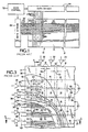
- Figs. 1-3 show a flat panel display system 10, which implements a prior art plasma addressing structure that includes a set of elongated cathodes 62 with respect to which the present invention may be implemented.
- flat panel display system 10 comprises a display panel 12 having a display surface 14 that contains a pattern formed by a rectangular planar array of nominally identical data storage or display elements ("pixels") 16 mutually spaced apart by predetermined distances in the vertical and horizontal directions.
- pixels data storage or display elements
- Electrodes 18 are hereinafter referred to as "column electrodes 18." All of the display elements or pixels 16 of a particular plasma channel 20 are set simultaneously when the inert gas in the plasma channel is sufficiently ionized. Each pixel is set to the potential gradient between the column electrode and ground at this time.
- column electrodes 18 and plasma channels 20 determine the dimensions of display elements 16, which are of rectangular shape.
- Column electrodes 18 are deposited on a major surface of a first electrically nonconductive, optically transparent substrate, and plasma channels 20 are inscribed in a major surface of a second electrically nonconductive, optically transparent substrate. Skilled persons will appreciate that certain systems, such as a reflective display of either the direct view or projection type, would require that only one of the substrates be optically transparent.
- Column electrodes 18 receive data drive signals of the analog voltage type developed on parallel output conductors 22' by different ones of the output amplifiers 22 (Figs. 2 and 3) of a data driver or drive circuit 24, and plasma channels 20 receive data strobe signals of the voltage pulse type developed on output conductors 26' by different ones of the output amplifiers 26 (Figs. 2 and 3) from the output of strobe circuit 28.
- Each of the plasma channels 20 includes a reference electrode 30 (Figs. 2 and 3) to which a reference potential common to each channel 20 and data strobe 28 is applied.
- display system 10 employs a scan control circuit 32 that coordinates the functions of data driver 24 and data strobe 28 so that all columns of display elements 16 of display panel 12 are addressed row by row in row scan fashion.
- Display panel 12 may employ electro-optic materials of different types. For example, if it uses such a material that changes the polarization state of incident light rays 33 (Fig. 3), display panel 12 is positioned between a pair of light polarizing filters 34 and 36 (Fig. 2), which cooperate with display panel 12 to change the luminance of light propagating through them.
- the use of a scattering liquid crystal cell as the electro-optic material would not require the use of polarizing filters 34 and 36, however.
- a color filter (not shown) may be positioned within display panel 12 to develop multi-colored images of controllable color intensity. For a projection display, color can also be achieved by using three separate monochrome panels 10, each of which controls one primary color.
- display panel 12 comprises an addressing structure that includes a pair of generally parallel electrode structures 40 and 42 spaced apart by a layer 44 of electro-optic material, such as a nematic liquid crystal, and a thin layer 46 of a dielectric material, such as glass, mica, or plastic.
- Electrode structure 40 comprises a glass dielectric substrate 48 that has deposited on its inner surface 50 column electrodes 18 of indium tin oxide, which is optically transparent, to form a striped pattern. Adjacent pairs of column electrodes 18 are spaced apart a distance 52, which defines the horizontal space between next adjacent display elements 16 in a row.
- Electrode structure 42 comprises a glass dielectric substrate 54 into whose top surface 56 multiple plasma channels 20 of trapezoidal cross section with rounded side walls are inscribed. Plasma channels 20 have a depth 58 measured from top surface 56 to a base portion 60. Each one of the plasma channels 20 has an anode electrode 30 and cathode electrode 62, both of which are thin and narrow. Each of these electrodes extend along base portion 60 and one out of a pair of inner side walls 64 which diverge in the direction away from base portion 60 toward inner surface 56.
- the anode electrodes 30 of the plasma channels 20 are connected to a common electrical reference potential, which can be fixed at ground potential as shown.
- the cathode electrodes 62 of the plasma channels 20 are connected to different ones of the output amplifiers 26 (of which three and five are shown in Fig. 2 and Fig. 3, respectively) of data strobe 28.
- the anode electrodes 30 and cathode electrodes 62 preferably are connected to the electrical reference potentials and the amplified outputs 26' of data strobe 28, respectively, on opposite edges of display panel 10.
- the sidewalls 64 between adjacent plasma channels 20 define a plurality of support structures 66 whose top surfaces 56 support layer 46 of dielectric material. Adjacent plasma channels 20 are spaced apart by the width 68 of the top portion of each support structure 66, which width 68 defines the vertical space between next adjacent display elements 16 in a column.
- the overlapping regions 70 of column electrodes 18 and plasma channels 20 define the dimensions of display elements 16, which are shown in dashed lines in Figs. 2 and 3. Fig. 3 shows with better clarity the array of display elements 16 and the vertical and horizontal spacings between them.
- the magnitude of the voltage applied to column electrodes 18 specifies the distance 52 to promote isolation of adjacent column electrodes 18.
- Distance 52 is typically much less than the width of column electrodes 18.
- the inclinations of the side walls 64 between adjacent plasma channels 20 specify the distance 68, which is typically much less than the width of plasma channels 20.
- the widths of the column electrodes 18 and the plasma channels 20 are typically the same and are a function of the desired image resolution, which is specified by the display application. It is desirable to make distances 52 and 68 as small as possible. In current models of display panel 12, the channel depth 58 is approximately one-half the channel width.
- Each of the plasma channels 20 is filled with an ionizable gaseous mixture, generally a mixture of inert gasses.
- Layer 46 of dielectric material functions as an isolating barrier between the ionizable gaseous mixture contained within channel 20 and layer 44 of liquid crystal material. The absence of dielectric layer 46 would, however, permit either the liquid crystal material to flow into the channel 20 or the ionizable gaseous mixture to contaminate the liquid crystal material. Dielectric layer 46 may be eliminated from displays that employ a solid or encapsulated electro-optic material.
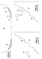
- Fig. 4 shows in greater detail prior art plasma channel 20 formed in glass substrate 54.
- Channel 20 is 450 microns wide at the top, 200 microns deep, and approximately 300 microns wide at the bottom.
- Cathode electrode 62 is about 75 microns wide and has a 0.2 micron thick bottom layer 72 of chromium for good adhesion to glass substrate 54, an approximately 2.0 micron thick layer of copper 74 for good conductance, and a 0.2 micron thick top layer 76 of chromium for sealing the copper layer 74 against oxidation. Skilled persons will appreciate that copper is highly electrically conductive and chromium is electrically conductive and gas impermeable.
- Anode electrode 30 may have an appearance and structure generally similar to that of cathode electrode 62.
- Figs. 5 and 6 show that top chromium layer 76 is susceptible to sputter damage.
- an ion 78 of inert gas is shown propagating toward the wavy surface 80 of top layer 76 of chromium in prior art cathode 62.
- Fig. 6 shows the results of the collision of ion 78 with surface 80 from which a chromium atom 82 has been dislodged and ion 78 has been deflected. Over time the dislodged chromium atoms 82 become deposited in increasing number on the sides and bottom of channel 20 and on the cover, turning a transmissive display system 10 dark and destroying its usefulness. Further, the chromium deposited on sheet 46 eventually renders its surface sufficiently conductive that it will no longer store different amounts of charge on various pixels 16 so that the lines of the display become uniformly gray.
- Fig. 7 is a cross-sectional view of a plasma channel 120 display undergoing an electrophoresis process conducted according to the present invention.
- like components are labelled with the same reference numerals as those in Figs. 1-6, except that 100 has been added to each reference numeral.
- Electrophoresis is a well known technique, and the electrophoresis techniques used in this invention are standard and known to skilled persons.
- Positively charged particles 184 of a refractory compound are suspended in a bath of a dielectric liquid such as isopropyl alcohol. Frit particles 186 also positively charged, are shown similarly suspended. A negative potential applied to cathode 162 draws these positively charged particles toward cathode 162. (Typically the same negative potential is applied to all electrodes in the channel during deposition.)
- Fig. 8 shows a cross-sectional view of the channel of Fig. 7 after the completion of electrophoresis.
- layer 176 of chromium On top of layer 176 of chromium, a new layer 188 of refractory compound particles 184 is intermixed with frit particles. This new layer is approximately 10.0 microns thick. Because top layer 188 of particles is discontinuous and is not air tight, layer 176 of chromium is still used to prevent oxidation of copper layer 174. Layer 176 of chromium extends along the entire length of copper layer 174 and therefore along the entire length of cathode 162.
- Fig. 9 shows a cross-sectional view of the channel of Fig. 7 after the completion of the air bake.
- the frit particles 186 have fused into a layer of glass 190, thereby cementing the refractory particles 184 to the electrode surface and to each other.
- Refractory materials are characterized by high heats of sublimation so that impinging gas ions colliding with them tend not to sublimate or dislodge any molecules of the refractory materials.
- the refractory compounds used are chosen for their oxidation resistance during the one hour air bake that is part of the manufacturing process.
- the refractory materials used were chosen for their low work functions.
- the probability of secondary electron emission by either an ionized or an excited gas atom is enhanced when the work function of the refractory material is low.
- fewer excited or ionized gas atoms are required in order to generate a given quantity of secondary electrons when the work function of the electrode surface is low. Because of these characteristics, it is possible to operate the PALC display with a lower potential gradient applied between its anode and the cathode electrode pairs. Under these operating conditions, a less intense electric field accelerates the ions, thereby leading to lower ion energies and less sputter damage.
- refractory compounds or combination of refractory compounds will work in the current invention. It is believed, however, that a compound from the group of rare earth hexaborides, particularly LaB 6 , YB 6 , GdB 6 or CeB 6 will provide superior performance compared with most other refractory compounds.
- Yttrium hexaboride YB 6
- Yttrium is counted among the rare earth hexaborides.
- Yttrium is not technically a member of the rare earth group of elements, it shares many of the characteristics of this group.
- Two other refractory compounds, Cr 3 Si and diamond may also provide good performance in this application.
- the compounds LaB 6 and GdB 6 have been experimentally verified to perform very well.
- an experiment may be conducted in which the compound is used in the fabrication of the plasma electrodes of a PALC display and then the display is run to determine the length of operating time necessary to provoke a set level of sputter damage.
Landscapes
- Engineering & Computer Science (AREA)
- Physics & Mathematics (AREA)
- Chemical & Material Sciences (AREA)
- Plasma & Fusion (AREA)
- Manufacturing & Machinery (AREA)
- Crystallography & Structural Chemistry (AREA)
- Materials Engineering (AREA)
- Gas-Filled Discharge Tubes (AREA)
- Liquid Crystal (AREA)
- Devices For Indicating Variable Information By Combining Individual Elements (AREA)
Applications Claiming Priority (2)
| Application Number | Priority Date | Filing Date | Title |
|---|---|---|---|
| US52099695A | 1995-08-30 | 1995-08-30 | |
| US520996 | 1995-08-30 |
Publications (2)
| Publication Number | Publication Date |
|---|---|
| EP0762460A2 true EP0762460A2 (fr) | 1997-03-12 |
| EP0762460A3 EP0762460A3 (fr) | 1998-04-15 |
Family
ID=24074910
Family Applications (1)
| Application Number | Title | Priority Date | Filing Date |
|---|---|---|---|
| EP96305962A Ceased EP0762460A3 (fr) | 1995-08-30 | 1996-08-15 | Revêtements conducteurs résistants à la pulvérisation et à faible potentiel de sortie pour des électrodes cathodiques dans une structure d'adressage par plasma en courant continu |
Country Status (5)
| Country | Link |
|---|---|
| US (2) | US5783906A (fr) |
| EP (1) | EP0762460A3 (fr) |
| JP (1) | JPH09311647A (fr) |
| KR (1) | KR100250541B1 (fr) |
| TW (1) | TW368671B (fr) |
Cited By (4)
| Publication number | Priority date | Publication date | Assignee | Title |
|---|---|---|---|---|
| WO1998052179A1 (fr) * | 1997-05-09 | 1998-11-19 | Koninklijke Philips Electronics N.V. | Dispositif d'affichage |
| WO1999004408A1 (fr) * | 1997-07-18 | 1999-01-28 | Koninklijke Philips Electronics N.V. | Dispositif d'affichage |
| WO1999033046A1 (fr) * | 1997-12-19 | 1999-07-01 | Koninklijke Philips Electronics N.V. | Dispositif d'affichage |
| EP0827176A3 (fr) * | 1996-08-16 | 2000-03-08 | Tektronix, Inc. | Revêtements conducteurs résistants à la pulvérisation à émission augmentée pour des électrodes cathodiques dans une structure d'adressage par plasma en courant continu |
Families Citing this family (19)
| Publication number | Priority date | Publication date | Assignee | Title |
|---|---|---|---|---|
| TW368671B (en) * | 1995-08-30 | 1999-09-01 | Tektronix Inc | Sputter-resistant, low-work-function, conductive coatings for cathode electrodes in DC plasma addressing structure |
| US5990619A (en) * | 1996-03-28 | 1999-11-23 | Tektronix, Inc. | Electrode structures for plasma addressed liquid crystal display devices |
| US6137550A (en) * | 1996-09-30 | 2000-10-24 | Tektronix, Inc. | Structure for a PALC display panel having a helium filling doped with hydrogen |
| US5948228A (en) * | 1996-10-11 | 1999-09-07 | Tektronix, Inc. | Method of fabricating a channel member for a PALC display panel |
| US6028572A (en) * | 1996-12-13 | 2000-02-22 | Tektronix, Inc. | Structure for a PALC display panel having a helium filling doped with hydrogen |
| US5939827A (en) * | 1996-12-13 | 1999-08-17 | Tektronix, Inc. | Non-reactive cathode for a PALC display panel using hydrogen-doped helium gas |
| US6110562A (en) * | 1996-12-13 | 2000-08-29 | Tektronix, Inc. | Conductive anode for a PALC display panel using hydrogen-doped helium gas |
| JPH10282896A (ja) * | 1997-04-07 | 1998-10-23 | Mitsubishi Electric Corp | 表示装置 |
| KR100430664B1 (ko) * | 1997-10-03 | 2004-06-16 | 가부시끼가이샤 히다치 세이사꾸쇼 | 가스방전형표시장치의제조방법 |
| US6252353B1 (en) * | 1997-12-17 | 2001-06-26 | Lg Electronics Inc. | Color plasma display panel |
| US6342755B1 (en) | 1999-08-11 | 2002-01-29 | Sony Corporation | Field emission cathodes having an emitting layer comprised of electron emitting particles and insulating particles |
| WO2001018840A1 (fr) * | 1999-09-08 | 2001-03-15 | Koninklijke Philips Electronics N.V. | Afficheur d'images a protection d'electrode |
| US6384520B1 (en) | 1999-11-24 | 2002-05-07 | Sony Corporation | Cathode structure for planar emitter field emission displays |
| JP2002075227A (ja) | 2000-06-14 | 2002-03-15 | Sharp Corp | 気体放電表示装置およびプラズマアドレス液晶表示装置ならびにその製造方法 |
| US8223101B1 (en) * | 2007-10-30 | 2012-07-17 | Copytele, Inc. | Active matrix phosphor cold cathode display |
| DE112006002464T5 (de) * | 2005-09-14 | 2008-07-24 | Littelfuse, Inc., Des Plaines | Gasgefüllter Überspannungsableiter, aktivierende Verbindung, Zündstreifen und Herstellungsverfahren dafür |
| JP2009170192A (ja) * | 2008-01-15 | 2009-07-30 | Panasonic Corp | プラズマディスプレイパネル |
| JP2009218023A (ja) * | 2008-03-10 | 2009-09-24 | Panasonic Corp | プラズマディスプレイパネル |
| US9978568B2 (en) * | 2013-08-12 | 2018-05-22 | Tokyo Electron Limited | Self-sustained non-ambipolar direct current (DC) plasma at low power |
Family Cites Families (23)
| Publication number | Priority date | Publication date | Assignee | Title |
|---|---|---|---|---|
| US3716742A (en) * | 1970-03-03 | 1973-02-13 | Fujitsu Ltd | Display device utilization gas discharge |
| CA1048182A (fr) * | 1976-10-26 | 1979-02-06 | Her Majesty The Queen, In Right Of Canada, As Represented By The Minister Of National Defence | Affichage au plasma commande par laser |
| DE3106368C2 (de) * | 1980-02-22 | 1987-04-09 | Okaya Electric Industries Co, Ltd., Tokio/Tokyo | Gleichstrom-Gasentladungsanzeigevorrichtung |
| US4340840A (en) * | 1980-04-21 | 1982-07-20 | International Business Machines Corporation | DC Gas discharge display panel with internal memory |
| JPS57180046A (en) * | 1981-04-28 | 1982-11-05 | Okaya Denki Sangyo Kk | Panel for displaying dc gas discharge |
| JPS60221928A (ja) * | 1984-04-19 | 1985-11-06 | Sony Corp | 放電表示装置の製造方法 |
| JPS60221926A (ja) * | 1984-04-19 | 1985-11-06 | Sony Corp | 放電表示装置の製造方法 |
| KR870002196B1 (ko) * | 1984-12-13 | 1987-12-28 | 주식회사 금성사 | 플라스마 표시장치 |
| US4896149A (en) * | 1988-01-19 | 1990-01-23 | Tektronix, Inc. | Addressing structure using ionizable gaseous medium |
| US5077553A (en) * | 1988-01-19 | 1991-12-31 | Tektronix, Inc. | Apparatus for and methods of addressing data storage elements |
| JPH0572518A (ja) * | 1991-09-11 | 1993-03-26 | Sony Corp | プラズマアドレス表示装置 |
| US5428263A (en) * | 1992-01-07 | 1995-06-27 | Mitsubishi Denki Kabushiki Kaisha | Discharge cathode device with stress relieving layer and method for manufacturing the same |
| FR2687839B1 (fr) * | 1992-02-26 | 1994-04-08 | Commissariat A Energie Atomique | Source d'electrons a cathodes emissives a micropointes et dispositif de visualisation par cathodoluminescence excitee par emission de champ utilisant cette source. |
| US5449970A (en) * | 1992-03-16 | 1995-09-12 | Microelectronics And Computer Technology Corporation | Diode structure flat panel display |
| TW228592B (fr) * | 1992-08-26 | 1994-08-21 | Tektronix Inc | |
| US5440201A (en) * | 1992-08-26 | 1995-08-08 | Tektronix, Inc. | Plasma addressing structure with wide or transparent reference electrode |
| JPH06223725A (ja) * | 1993-01-27 | 1994-08-12 | Mitsubishi Electric Corp | 気体放電表示装置 |
| US5402145A (en) * | 1993-02-17 | 1995-03-28 | Copytele, Inc. | Electrophoretic display panel with arc driven individual pixels |
| US5461395A (en) * | 1993-03-08 | 1995-10-24 | Tektronix, Inc. | Plasma addressing structure having a pliant dielectric layer |
| GB9313841D0 (en) * | 1993-07-05 | 1993-08-18 | Philips Electronics Uk Ltd | An electro-optic device |
| SG64844A1 (en) * | 1994-07-21 | 1999-05-25 | Sony Corp | Plasma-addressed display device |
| TW368671B (en) * | 1995-08-30 | 1999-09-01 | Tektronix Inc | Sputter-resistant, low-work-function, conductive coatings for cathode electrodes in DC plasma addressing structure |
| JP3765901B2 (ja) * | 1996-02-26 | 2006-04-12 | 株式会社東芝 | プラズマディスプレイ及びプラズマ液晶ディスプレイ |
-
1996
- 1996-08-12 TW TW085109774A patent/TW368671B/zh active
- 1996-08-15 EP EP96305962A patent/EP0762460A3/fr not_active Ceased
- 1996-08-20 KR KR1019960034437A patent/KR100250541B1/ko not_active Expired - Fee Related
- 1996-08-27 JP JP8244083A patent/JPH09311647A/ja active Pending
-
1997
- 1997-06-06 US US08/870,763 patent/US5783906A/en not_active Expired - Fee Related
- 1997-07-31 US US08/904,154 patent/US5917284A/en not_active Expired - Fee Related
Cited By (5)
| Publication number | Priority date | Publication date | Assignee | Title |
|---|---|---|---|---|
| EP0827176A3 (fr) * | 1996-08-16 | 2000-03-08 | Tektronix, Inc. | Revêtements conducteurs résistants à la pulvérisation à émission augmentée pour des électrodes cathodiques dans une structure d'adressage par plasma en courant continu |
| WO1998052179A1 (fr) * | 1997-05-09 | 1998-11-19 | Koninklijke Philips Electronics N.V. | Dispositif d'affichage |
| WO1999004408A1 (fr) * | 1997-07-18 | 1999-01-28 | Koninklijke Philips Electronics N.V. | Dispositif d'affichage |
| US6052160A (en) * | 1997-07-18 | 2000-04-18 | U.S. Philips Corporation | Display device with sputter-resistant electrode layer for providing plasma discharge |
| WO1999033046A1 (fr) * | 1997-12-19 | 1999-07-01 | Koninklijke Philips Electronics N.V. | Dispositif d'affichage |
Also Published As
| Publication number | Publication date |
|---|---|
| US5917284A (en) | 1999-06-29 |
| JPH09311647A (ja) | 1997-12-02 |
| KR970012899A (ko) | 1997-03-29 |
| EP0762460A3 (fr) | 1998-04-15 |
| KR100250541B1 (ko) | 2000-07-01 |
| US5783906A (en) | 1998-07-21 |
| TW368671B (en) | 1999-09-01 |
Similar Documents
| Publication | Publication Date | Title |
|---|---|---|
| US5783906A (en) | Sputter-resistant, low-work-function, conductive coatings for cathode electrodes in DC plasma addressing structure | |
| CA2104193C (fr) | Configuration d'electrode bicanal utilisant un gaz ionisable pour structure d'adressage et methode d'utilisation de cette configuration | |
| KR100260580B1 (ko) | 교류에너지원에 의해 여기되는 이온화가능한 가스에 의한 데이터 기억소자의 어드레스지정장치 | |
| EP0545642B1 (fr) | Tubes afficheurs à décharge | |
| US5276384A (en) | Electrode configuration for channel confinement of plasma discharge in an electrode structure using an ionizable gaseous medium | |
| HK1004350B (en) | Apparatus for addressing data storage elements with an ionizable gas excited by an ac energy source | |
| JP2571522B2 (ja) | プラズマ・アドレス指定装置 | |
| US5990619A (en) | Electrode structures for plasma addressed liquid crystal display devices | |
| US5868811A (en) | Method of making a channel plate for a flat display device | |
| US5705886A (en) | Cathode for plasma addressed liquid crystal display | |
| US6007399A (en) | Hollow cathodes for plasma-containing display devices and method of producing same | |
| US6052160A (en) | Display device with sputter-resistant electrode layer for providing plasma discharge | |
| EP0614167B1 (fr) | Shunt d'électrodes dans un canal avec plasma | |
| EP0023082A1 (fr) | Dispositif d'affichage et methode de mise en oeuvre | |
| US5956002A (en) | Structures and methods for limiting current in ionizable gaseous medium devices | |
| EP0827176A2 (fr) | Revêtements conducteurs résistants à la pulvérisation à émission augmentée pour des électrodes cathodiques dans une structure d'adressage par plasma en courant continu | |
| KR940004296B1 (ko) | 플라즈마 어드레스 방식의 액정표시소자 | |
| NL1005646C2 (nl) | Werkwijze en toestel voor het reduceren van de stroomopname in een plasma-geadresseerde structuur. | |
| CN1177824A (zh) | 直流等离子体寻址结构中的抗溅射低脱出功的阴极电极导电涂层 | |
| JPH09179105A (ja) | プラズマアドレス方式表示素子及びその駆動装置 | |
| JPH11311774A (ja) | プラズマアドレス表示装置 |
Legal Events
| Date | Code | Title | Description |
|---|---|---|---|
| PUAI | Public reference made under article 153(3) epc to a published international application that has entered the european phase |
Free format text: ORIGINAL CODE: 0009012 |
|
| AK | Designated contracting states |
Kind code of ref document: A2 Designated state(s): DE FR GB IT |
|
| PUAL | Search report despatched |
Free format text: ORIGINAL CODE: 0009013 |
|
| AK | Designated contracting states |
Kind code of ref document: A3 Designated state(s): DE FR GB IT |
|
| 17P | Request for examination filed |
Effective date: 19981012 |
|
| 17Q | First examination report despatched |
Effective date: 19990504 |
|
| GRAG | Despatch of communication of intention to grant |
Free format text: ORIGINAL CODE: EPIDOS AGRA |
|
| STAA | Information on the status of an ep patent application or granted ep patent |
Free format text: STATUS: THE APPLICATION HAS BEEN REFUSED |
|
| 18R | Application refused |
Effective date: 20020527 |