EP0762533A2 - Antennenanordnung - Google Patents
Antennenanordnung Download PDFInfo
- Publication number
- EP0762533A2 EP0762533A2 EP96113583A EP96113583A EP0762533A2 EP 0762533 A2 EP0762533 A2 EP 0762533A2 EP 96113583 A EP96113583 A EP 96113583A EP 96113583 A EP96113583 A EP 96113583A EP 0762533 A2 EP0762533 A2 EP 0762533A2
- Authority
- EP
- European Patent Office
- Prior art keywords
- antenna
- capacitance
- antenna apparatus
- generating device
- conductor
- Prior art date
- Legal status (The legal status is an assumption and is not a legal conclusion. Google has not performed a legal analysis and makes no representation as to the accuracy of the status listed.)
- Granted
Links
Images


Classifications
-
- H—ELECTRICITY
- H01—ELECTRIC ELEMENTS
- H01Q—ANTENNAS, i.e. RADIO AERIALS
- H01Q1/00—Details of, or arrangements associated with, antennas
- H01Q1/36—Structural form of radiating elements, e.g. cone, spiral, umbrella; Particular materials used therewith
-
- H—ELECTRICITY
- H01—ELECTRIC ELEMENTS
- H01Q—ANTENNAS, i.e. RADIO AERIALS
- H01Q1/00—Details of, or arrangements associated with, antennas
- H01Q1/36—Structural form of radiating elements, e.g. cone, spiral, umbrella; Particular materials used therewith
- H01Q1/38—Structural form of radiating elements, e.g. cone, spiral, umbrella; Particular materials used therewith formed by a conductive layer on an insulating support
-
- H—ELECTRICITY
- H05—ELECTRIC TECHNIQUES NOT OTHERWISE PROVIDED FOR
- H05K—PRINTED CIRCUITS; CASINGS OR CONSTRUCTIONAL DETAILS OF ELECTRIC APPARATUS; MANUFACTURE OF ASSEMBLAGES OF ELECTRICAL COMPONENTS
- H05K1/00—Printed circuits
- H05K1/02—Details
- H05K1/0213—Electrical arrangements not otherwise provided for
- H05K1/0216—Reduction of cross-talk, noise or electromagnetic interference
- H05K1/023—Reduction of cross-talk, noise or electromagnetic interference using auxiliary mounted passive components or auxiliary substances
- H05K1/0231—Capacitors or dielectric substances
-
- H—ELECTRICITY
- H05—ELECTRIC TECHNIQUES NOT OTHERWISE PROVIDED FOR
- H05K—PRINTED CIRCUITS; CASINGS OR CONSTRUCTIONAL DETAILS OF ELECTRIC APPARATUS; MANUFACTURE OF ASSEMBLAGES OF ELECTRICAL COMPONENTS
- H05K1/00—Printed circuits
- H05K1/02—Details
- H05K1/0213—Electrical arrangements not otherwise provided for
- H05K1/0237—High frequency adaptations
- H05K1/0243—Printed circuits associated with mounted high frequency components
-
- H—ELECTRICITY
- H05—ELECTRIC TECHNIQUES NOT OTHERWISE PROVIDED FOR
- H05K—PRINTED CIRCUITS; CASINGS OR CONSTRUCTIONAL DETAILS OF ELECTRIC APPARATUS; MANUFACTURE OF ASSEMBLAGES OF ELECTRICAL COMPONENTS
- H05K1/00—Printed circuits
- H05K1/02—Details
- H05K1/0213—Electrical arrangements not otherwise provided for
- H05K1/0216—Reduction of cross-talk, noise or electromagnetic interference
- H05K1/0218—Reduction of cross-talk, noise or electromagnetic interference by printed shielding conductors, ground planes or power plane
- H05K1/0219—Printed shielding conductors for shielding around or between signal conductors, e.g. coplanar or coaxial printed shielding conductors
-
- H—ELECTRICITY
- H05—ELECTRIC TECHNIQUES NOT OTHERWISE PROVIDED FOR
- H05K—PRINTED CIRCUITS; CASINGS OR CONSTRUCTIONAL DETAILS OF ELECTRIC APPARATUS; MANUFACTURE OF ASSEMBLAGES OF ELECTRICAL COMPONENTS
- H05K1/00—Printed circuits
- H05K1/02—Details
- H05K1/11—Printed elements for providing electric connections to or between printed circuits
- H05K1/111—Pads for surface mounting, e.g. lay-out
-
- H—ELECTRICITY
- H05—ELECTRIC TECHNIQUES NOT OTHERWISE PROVIDED FOR
- H05K—PRINTED CIRCUITS; CASINGS OR CONSTRUCTIONAL DETAILS OF ELECTRIC APPARATUS; MANUFACTURE OF ASSEMBLAGES OF ELECTRICAL COMPONENTS
- H05K1/00—Printed circuits
- H05K1/16—Printed circuits incorporating printed electric components, e.g. printed resistors, capacitors or inductors
- H05K1/162—Printed circuits incorporating printed electric components, e.g. printed resistors, capacitors or inductors incorporating printed capacitors
-
- H—ELECTRICITY
- H05—ELECTRIC TECHNIQUES NOT OTHERWISE PROVIDED FOR
- H05K—PRINTED CIRCUITS; CASINGS OR CONSTRUCTIONAL DETAILS OF ELECTRIC APPARATUS; MANUFACTURE OF ASSEMBLAGES OF ELECTRICAL COMPONENTS
- H05K2201/00—Indexing scheme relating to printed circuits covered by H05K1/00
- H05K2201/09—Shape and layout
- H05K2201/09209—Shape and layout details of conductors
- H05K2201/09218—Conductive traces
- H05K2201/09236—Parallel layout
-
- H—ELECTRICITY
- H05—ELECTRIC TECHNIQUES NOT OTHERWISE PROVIDED FOR
- H05K—PRINTED CIRCUITS; CASINGS OR CONSTRUCTIONAL DETAILS OF ELECTRIC APPARATUS; MANUFACTURE OF ASSEMBLAGES OF ELECTRICAL COMPONENTS
- H05K2201/00—Indexing scheme relating to printed circuits covered by H05K1/00
- H05K2201/10—Details of components or other objects attached to or integrated in a printed circuit board
- H05K2201/10431—Details of mounted components
- H05K2201/10507—Involving several components
- H05K2201/10522—Adjacent components
-
- H—ELECTRICITY
- H05—ELECTRIC TECHNIQUES NOT OTHERWISE PROVIDED FOR
- H05K—PRINTED CIRCUITS; CASINGS OR CONSTRUCTIONAL DETAILS OF ELECTRIC APPARATUS; MANUFACTURE OF ASSEMBLAGES OF ELECTRICAL COMPONENTS
- H05K2201/00—Indexing scheme relating to printed circuits covered by H05K1/00
- H05K2201/10—Details of components or other objects attached to or integrated in a printed circuit board
- H05K2201/10613—Details of electrical connections of non-printed components, e.g. special leads
- H05K2201/10621—Components characterised by their electrical contacts
- H05K2201/10636—Leadless chip, e.g. chip capacitor or resistor
-
- H—ELECTRICITY
- H05—ELECTRIC TECHNIQUES NOT OTHERWISE PROVIDED FOR
- H05K—PRINTED CIRCUITS; CASINGS OR CONSTRUCTIONAL DETAILS OF ELECTRIC APPARATUS; MANUFACTURE OF ASSEMBLAGES OF ELECTRICAL COMPONENTS
- H05K3/00—Apparatus or processes for manufacturing printed circuits
- H05K3/30—Assembling printed circuits with electric components, e.g. with resistors
- H05K3/32—Assembling printed circuits with electric components, e.g. with resistors electrically connecting electric components or wires to printed circuits
- H05K3/34—Assembling printed circuits with electric components, e.g. with resistors electrically connecting electric components or wires to printed circuits by soldering
- H05K3/341—Surface mounted components
- H05K3/3431—Leadless components
- H05K3/3442—Leadless components having edge contacts, e.g. leadless chip capacitors, chip carriers
-
- Y—GENERAL TAGGING OF NEW TECHNOLOGICAL DEVELOPMENTS; GENERAL TAGGING OF CROSS-SECTIONAL TECHNOLOGIES SPANNING OVER SEVERAL SECTIONS OF THE IPC; TECHNICAL SUBJECTS COVERED BY FORMER USPC CROSS-REFERENCE ART COLLECTIONS [XRACs] AND DIGESTS
- Y02—TECHNOLOGIES OR APPLICATIONS FOR MITIGATION OR ADAPTATION AGAINST CLIMATE CHANGE
- Y02P—CLIMATE CHANGE MITIGATION TECHNOLOGIES IN THE PRODUCTION OR PROCESSING OF GOODS
- Y02P70/00—Climate change mitigation technologies in the production process for final industrial or consumer products
- Y02P70/50—Manufacturing or production processes characterised by the final manufactured product
Definitions
- the present invention relates to an antenna apparatus for use in mobile communications and local area networks (LAN).
- LAN local area networks
- a conventional antenna apparatus generally designated by 50 includes a chip antenna 51, a mounting board 52 on which the chip antenna 51 is mounted, a ground pattern 53 formed on the board 52, and a microstrip line 54 also formed on the board 52.
- This chip antenna 51 is formed, as shown in the longitudinal cross-sectional view of Fig. 12, of an insulator 55, a coil-like conductor 56, a magnetic substance 57, and external connecting terminals 58a and 58b.
- the antenna apparatus of the above conventional type encounters the following problem. Namely, when the chip antenna is mounted on the board, the resonant frequency and the impedance of the chip antenna disadvantageously deviate from the determined values depending on the material of the board, the configuration of the ground pattern, the material of a casing for accommodating the apparatus therein, and other conditions.
- the resonant frequency of the chip antenna is adjustable in advance allowing for deviations, while the impedance is unadjustable.
- an antenna apparatus comprising: a chip antenna having a substrate, at least one conductor formed on at least one of a surface portion and an inside portion of the substrate, and at least one feeding terminal disposed on the surface of the substrate so as to apply a voltage to the conductor; a mounting board including a ground pattern, for mounting the chip antenna on the board; and a capacitance-generating device disposed between the feeding terminal of the chip antenna and the ground pattern of the mounting board.
- the capacitance-generating device may comprise a dielectric resin, a capacitor or an open stub.
- the provision of the capacitance-generating device makes it possible to adjust the impedance of the apparatus.
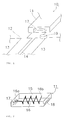
- an antenna apparatus generally designated by 10 includes a chip antenna 11, a mounting board 12 on which the chip antenna 11 is mounted, a ground pattern 13, and a microstrip line 14, both the pattern 13 and the line 14 being formed on the board 12.
- the chip antenna 11 is packaged within a rectangular prism-shaped dielectric substrate 15 essentially consisting of titanium oxide and barium oxide and comprises, as illustrated in Fig. 2, a conductor 16 that is spirally wound in or along the substrate 15 in its longitudinal direction, a feeding terminal 17 for applying a voltage to the surface of the substrate 15, and a mounting terminal 18 for securing the chip antenna 11 on the board 12.
- One end of the conductor 16 serves as a feeding end 16a connected to the feeding terminal 17, while the other end is free to form a free end 16b within the dielectric substrate 15.
- the feeding terminal 17 of the chip antenna 11 is connected to the microstrip line 14 formed on the board 12 by means of soldering (not shown), thereby forming the antenna apparatus 10.
- a capacitance-generating device i.e., a dielectric resin 19, is disposed between the microstrip line 14 connected to the terminal 17 of the antenna 11 and the ground pattern 13 so as to generate a capacitance between the microstrip line 14 and the ground pattern 13.
- FIG. 3 there is shown an antenna apparatus of a second embodiment of the present invention.
- the antenna apparatus generally designated by 20 differs from the antenna apparatus 10 of the first embodiment in that a capacitor 21 is used as the capacitance-generating device disposed between the microstrip line 14 connected to the feeding terminal 17 of the chip antenna 11 and the ground pattern 13. This capacitor 21 generates a capacitance between the microstrip line 14 and the ground pattern 13.
- Fig. 4 is a perspective view of an antenna apparatus according to a third embodiment of the present invention.
- the antenna apparatus generally indicated by 30 differs from the antenna apparatus 10 of the first embodiment in that an open stub 31 serves as the capacitance-generating device formed between a portion extending from the microstrip line 14 connected to the feeding terminal 17 of the chip antenna 11 and a grounding electrode (not shown) on the reverse surface of the ground pattern 13.
- This open stub 31 produces a capacitance between the microstrip line 14 and the ground pattern 13.
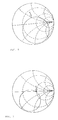
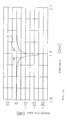
- Impedance characteristics of the antenna apparatus are shown in Figs. 5, 6 and 7, while insertion-loss characteristics of the apparatus are illustrated in Figs. 8, 9 and 10.
- Figs. 5 and 8 illustrate impedance characteristics and insertion-loss characteristics resulting from the apparatus without disposing capacitance-generating device
- Figs. 6 and 9 illustrate the above-described characteristics obtained from the apparatus provided with a capacitance-generating device having a capacitance of 1 pF
- Figs. 7 and 10 show the above-described characteristics obtained from the apparatus provided with a capacitance-generating device having a capacitance of 2 pF.
- Table 1 shows the impedances at the center frequency (1.9 GHz: indicated by the arrow 1 in Figs. 5 through 7) resulting from the characteristics shown in Figs. 5 through 7 and also indicates the bandwidths resulting from the characteristics shown in Figs. 8 through 10.
- Table 1 Impedance at the center frequency ( ⁇ ) Bandwidth of the antenna apparatuses (MHz) No capacitance-generating device 12.99 123.5 Capacitance-generating device of 1 pF 32.72 91.6 Capacitance-generating device of 2 pF 49.59 57.3
- the capacitance-generating device if a capacitor is used as the capacitance-generating device, only a small area is required for mounting the capacitor on the board, which makes it possible to select a desired capacitance. The costs of the apparatus can also be reduced.
- the capacitance of the open stub is adjustable by varying the area of the extending portion from the microstrip line, thereby obtaining a desired impedance.
- the provision of the capacitance-generating device makes it possible to obtain a desired impedance at the center frequency, whereby a desired bandwidth can also be acquired.
- the substrate of the chip antenna is formed of a dielectric material comprising mainly titanium oxide and barium oxide.
- the substrate of the chip antenna may be formed of a dielectric material comprising mainly aluminum oxide or silica, a magnetic material essentially comprising nickel, cobalt and iron, or a combination of a dielectric material and a magnetic material.
- a spiral conductor is formed within the substrate of the chip antenna, it may be formed on at least one of the surface portion and the inside portion of the substrate.
- a meander-like conductor may be formed on at least one of the surface portion and the inside portion of the substrate.
- the position of the feeding terminal defined in the above-described embodiments is not essential to carry out the present invention.
- the capacitance-generating device is disposed between the feeding terminal of the chip antenna and the microstrip line formed on the mounting board so as to obtain a desired impedance at the center frequency, thereby acquiring a desired bandwidth.
Landscapes
- Engineering & Computer Science (AREA)
- Microelectronics & Electronic Packaging (AREA)
- Physics & Mathematics (AREA)
- Electromagnetism (AREA)
- Details Of Aerials (AREA)
- Waveguide Aerials (AREA)
Applications Claiming Priority (3)
| Application Number | Priority Date | Filing Date | Title |
|---|---|---|---|
| JP214899/95 | 1995-08-23 | ||
| JP7214899A JPH0964628A (ja) | 1995-08-23 | 1995-08-23 | アンテナ装置 |
| JP21489995 | 1995-08-23 |
Publications (3)
| Publication Number | Publication Date |
|---|---|
| EP0762533A2 true EP0762533A2 (de) | 1997-03-12 |
| EP0762533A3 EP0762533A3 (de) | 1997-05-07 |
| EP0762533B1 EP0762533B1 (de) | 2004-11-24 |
Family
ID=16663411
Family Applications (1)
| Application Number | Title | Priority Date | Filing Date |
|---|---|---|---|
| EP96113583A Expired - Lifetime EP0762533B1 (de) | 1995-08-23 | 1996-08-23 | Antennenanpa schaltung |
Country Status (4)
| Country | Link |
|---|---|
| US (1) | US5767817A (de) |
| EP (1) | EP0762533B1 (de) |
| JP (1) | JPH0964628A (de) |
| DE (1) | DE69633892T2 (de) |
Cited By (7)
| Publication number | Priority date | Publication date | Assignee | Title |
|---|---|---|---|---|
| EP0828310A3 (de) * | 1996-09-10 | 1999-05-19 | Murata Manufacturing Co., Ltd. | Antennenvorrichtung |
| EP0878863A3 (de) * | 1997-05-14 | 2000-02-23 | Murata Manufacturing Co., Ltd. | Mobiles Funkgerät |
| EP1498985A1 (de) * | 2003-07-14 | 2005-01-19 | Ngk Spark Plug Co., Ltd | Antennenvorrichtung und Methode zur Herstellung dieser Vorrichtung |
| EP2107635A1 (de) * | 2008-03-31 | 2009-10-07 | TDK Corporation | Zweilagige Breitbandantenne |
| US7742001B2 (en) | 2008-03-31 | 2010-06-22 | Tdk Corporation | Two-tier wide band antenna |
| EP2092607A4 (de) * | 2006-10-05 | 2012-12-19 | Pulse Finland Oy | Mehrbandantenne mit einer gemeinsamen resonanz-zuführungsstruktur und verfahren |
| CN103138046A (zh) * | 2011-11-30 | 2013-06-05 | 美桀电子科技(深圳)有限公司 | 天线单元及其制造方法 |
Families Citing this family (9)
| Publication number | Priority date | Publication date | Assignee | Title |
|---|---|---|---|---|
| JPH09284029A (ja) * | 1996-04-16 | 1997-10-31 | Murata Mfg Co Ltd | チップアンテナ |
| JP2996191B2 (ja) * | 1996-12-25 | 1999-12-27 | 株式会社村田製作所 | チップアンテナ |
| JP3651553B2 (ja) * | 1998-04-10 | 2005-05-25 | 富士通株式会社 | モバイル型情報処理装置 |
| JP4635326B2 (ja) * | 2000-10-31 | 2011-02-23 | 株式会社村田製作所 | アンテナの実装構造およびそれを備えた無線装置 |
| US6995710B2 (en) * | 2001-10-09 | 2006-02-07 | Ngk Spark Plug Co., Ltd. | Dielectric antenna for high frequency wireless communication apparatus |
| KR100584317B1 (ko) * | 2004-02-06 | 2006-05-26 | 삼성전자주식회사 | 휴대용 단말기의 안테나 장치 |
| US8018397B2 (en) * | 2005-12-30 | 2011-09-13 | Industrial Technology Research Institute | High dielectric antenna substrate and antenna thereof |
| TWI351130B (en) * | 2005-12-30 | 2011-10-21 | Ind Tech Res Inst | High dielectric antenna substrate and antenna thereof |
| US8164167B2 (en) | 2007-03-09 | 2012-04-24 | Nanyang Technological University | Integrated circuit structure and a method of forming the same |
Family Cites Families (6)
| Publication number | Priority date | Publication date | Assignee | Title |
|---|---|---|---|---|
| US4445122A (en) * | 1981-03-30 | 1984-04-24 | Leuven Research & Development V.Z.W. | Broad-band microstrip antenna |
| EP0616383B1 (de) * | 1993-03-19 | 1997-12-03 | Ascom Business Systems Ag | Antennenanordnung für in der Hand tragbare Funkgeräte |
| DE69422327T2 (de) * | 1993-04-23 | 2000-07-27 | Murata Mfg. Co., Ltd. | Oberflächenmontierbare Antenneneinheit |
| JP3232895B2 (ja) * | 1994-08-05 | 2001-11-26 | 株式会社村田製作所 | 表面実装型アンテナ及びその周波数調整方法 |
| JP3235367B2 (ja) * | 1994-10-11 | 2001-12-04 | 株式会社村田製作所 | アンテナ装置 |
| EP0743699B1 (de) * | 1995-05-17 | 2001-09-12 | Murata Manufacturing Co., Ltd. | Oberflächenmontierbares Antennensystem |
-
1995
- 1995-08-23 JP JP7214899A patent/JPH0964628A/ja active Pending
-
1996
- 1996-08-22 US US08/701,594 patent/US5767817A/en not_active Expired - Fee Related
- 1996-08-23 DE DE69633892T patent/DE69633892T2/de not_active Expired - Fee Related
- 1996-08-23 EP EP96113583A patent/EP0762533B1/de not_active Expired - Lifetime
Cited By (11)
| Publication number | Priority date | Publication date | Assignee | Title |
|---|---|---|---|---|
| EP0828310A3 (de) * | 1996-09-10 | 1999-05-19 | Murata Manufacturing Co., Ltd. | Antennenvorrichtung |
| US5999146A (en) * | 1996-09-10 | 1999-12-07 | Murata Manufacturing Co., Ltd. | Antenna device |
| EP0878863A3 (de) * | 1997-05-14 | 2000-02-23 | Murata Manufacturing Co., Ltd. | Mobiles Funkgerät |
| EP1498985A1 (de) * | 2003-07-14 | 2005-01-19 | Ngk Spark Plug Co., Ltd | Antennenvorrichtung und Methode zur Herstellung dieser Vorrichtung |
| US7102574B2 (en) | 2003-07-14 | 2006-09-05 | Ngk Spark Plug Co., Ltd. | Antenna device and method for manufacturing the same |
| EP2092607A4 (de) * | 2006-10-05 | 2012-12-19 | Pulse Finland Oy | Mehrbandantenne mit einer gemeinsamen resonanz-zuführungsstruktur und verfahren |
| EP2107635A1 (de) * | 2008-03-31 | 2009-10-07 | TDK Corporation | Zweilagige Breitbandantenne |
| US7742001B2 (en) | 2008-03-31 | 2010-06-22 | Tdk Corporation | Two-tier wide band antenna |
| US7800543B2 (en) | 2008-03-31 | 2010-09-21 | Tdk Corporation | Feed-point tuned wide band antenna |
| CN103138046A (zh) * | 2011-11-30 | 2013-06-05 | 美桀电子科技(深圳)有限公司 | 天线单元及其制造方法 |
| CN103138046B (zh) * | 2011-11-30 | 2015-04-29 | 美桀电子科技(深圳)有限公司 | 天线单元及其制造方法 |
Also Published As
| Publication number | Publication date |
|---|---|
| DE69633892T2 (de) | 2005-11-24 |
| EP0762533B1 (de) | 2004-11-24 |
| US5767817A (en) | 1998-06-16 |
| EP0762533A3 (de) | 1997-05-07 |
| DE69633892D1 (de) | 2004-12-30 |
| JPH0964628A (ja) | 1997-03-07 |
Similar Documents
| Publication | Publication Date | Title |
|---|---|---|
| EP0762533A2 (de) | Antennenanordnung | |
| US5874926A (en) | Matching circuit and antenna apparatus | |
| JP3246440B2 (ja) | アンテナ装置およびそれを用いた通信機 | |
| US6271803B1 (en) | Chip antenna and radio equipment including the same | |
| KR100266376B1 (ko) | 표면 실장형 안테나 및 통신기기 | |
| JP3738577B2 (ja) | アンテナ装置及び移動体通信機器 | |
| EP0909024A2 (de) | Impedanzanpassungsgerät | |
| EP0777295A2 (de) | Antenne mit zwei Resonanzfrequenzen | |
| JP3232895B2 (ja) | 表面実装型アンテナ及びその周波数調整方法 | |
| EP0860896B1 (de) | Antennenvorrichtung | |
| JP3409069B2 (ja) | ワイヤレス通信装置のためのアンテナ・アセンブリ | |
| US5764198A (en) | Chip antenna | |
| EP0828310B1 (de) | Antennenvorrichtung | |
| US5668557A (en) | Surface-mount antenna and communication device using same | |
| KR0133523B1 (ko) | 용량성 트리밍 장치 | |
| JPH1098405A (ja) | アンテナ装置 | |
| JP3250479B2 (ja) | アンテナ装置 | |
| JPH04125903A (ja) | 高周波用終端抵抗器 | |
| JPH06338712A (ja) | 高周波集積回路 | |
| JP3296017B2 (ja) | アンテナ装置 | |
| JP2917316B2 (ja) | アンテナ | |
| JP3326762B2 (ja) | アンテナ装置 | |
| KR200228002Y1 (ko) | 광대역 슬리브 안테나 | |
| JPH02237302A (ja) | 同軸―マイクロストリップ線路変換器 | |
| JP4017137B2 (ja) | アンテナ素子及びそれを用いた無線通信装置 |
Legal Events
| Date | Code | Title | Description |
|---|---|---|---|
| PUAI | Public reference made under article 153(3) epc to a published international application that has entered the european phase |
Free format text: ORIGINAL CODE: 0009012 |
|
| 17P | Request for examination filed |
Effective date: 19960823 |
|
| AK | Designated contracting states |
Kind code of ref document: A2 Designated state(s): DE FR GB |
|
| PUAL | Search report despatched |
Free format text: ORIGINAL CODE: 0009013 |
|
| AK | Designated contracting states |
Kind code of ref document: A3 Designated state(s): DE FR GB |
|
| 17Q | First examination report despatched |
Effective date: 20000707 |
|
| GRAP | Despatch of communication of intention to grant a patent |
Free format text: ORIGINAL CODE: EPIDOSNIGR1 |
|
| RTI1 | Title (correction) |
Free format text: ANTENNA MATCHING DEVICE |
|
| GRAS | Grant fee paid |
Free format text: ORIGINAL CODE: EPIDOSNIGR3 |
|
| GRAA | (expected) grant |
Free format text: ORIGINAL CODE: 0009210 |
|
| AK | Designated contracting states |
Kind code of ref document: B1 Designated state(s): DE FR GB |
|
| REG | Reference to a national code |
Ref country code: GB Ref legal event code: FG4D |
|
| REF | Corresponds to: |
Ref document number: 69633892 Country of ref document: DE Date of ref document: 20041230 Kind code of ref document: P |
|
| PLBE | No opposition filed within time limit |
Free format text: ORIGINAL CODE: 0009261 |
|
| ET | Fr: translation filed | ||
| 26N | No opposition filed |
Effective date: 20050825 |
|
| PGFP | Annual fee paid to national office [announced via postgrant information from national office to epo] |
Ref country code: DE Payment date: 20070816 Year of fee payment: 12 |
|
| PGFP | Annual fee paid to national office [announced via postgrant information from national office to epo] |
Ref country code: GB Payment date: 20070822 Year of fee payment: 12 |
|
| PGFP | Annual fee paid to national office [announced via postgrant information from national office to epo] |
Ref country code: FR Payment date: 20070808 Year of fee payment: 12 |
|
| GBPC | Gb: european patent ceased through non-payment of renewal fee |
Effective date: 20080823 |
|
| REG | Reference to a national code |
Ref country code: FR Ref legal event code: ST Effective date: 20090430 |
|
| PG25 | Lapsed in a contracting state [announced via postgrant information from national office to epo] |
Ref country code: FR Free format text: LAPSE BECAUSE OF NON-PAYMENT OF DUE FEES Effective date: 20080901 Ref country code: DE Free format text: LAPSE BECAUSE OF NON-PAYMENT OF DUE FEES Effective date: 20090303 |
|
| PG25 | Lapsed in a contracting state [announced via postgrant information from national office to epo] |
Ref country code: GB Free format text: LAPSE BECAUSE OF NON-PAYMENT OF DUE FEES Effective date: 20080823 |