EP0762752A2 - Abtasten eines analogen Videosignals für sekundäre Bilder - Google Patents
Abtasten eines analogen Videosignals für sekundäre Bilder Download PDFInfo
- Publication number
- EP0762752A2 EP0762752A2 EP96113833A EP96113833A EP0762752A2 EP 0762752 A2 EP0762752 A2 EP 0762752A2 EP 96113833 A EP96113833 A EP 96113833A EP 96113833 A EP96113833 A EP 96113833A EP 0762752 A2 EP0762752 A2 EP 0762752A2
- Authority
- EP
- European Patent Office
- Prior art keywords
- sample
- samples
- secondary image
- pattern
- luminance
- Prior art date
- Legal status (The legal status is an assumption and is not a legal conclusion. Google has not performed a legal analysis and makes no representation as to the accuracy of the status listed.)
- Withdrawn
Links
- 238000005070 sampling Methods 0.000 title claims description 20
- 238000000034 method Methods 0.000 claims description 26
- 230000000750 progressive effect Effects 0.000 claims description 18
- 238000010586 diagram Methods 0.000 description 8
- 238000006243 chemical reaction Methods 0.000 description 7
- 230000006870 function Effects 0.000 description 6
- 230000008569 process Effects 0.000 description 6
- 239000000872 buffer Substances 0.000 description 5
- 238000012986 modification Methods 0.000 description 2
- 230000004048 modification Effects 0.000 description 2
- 238000000926 separation method Methods 0.000 description 2
- 230000005236 sound signal Effects 0.000 description 2
- 101000860173 Myxococcus xanthus C-factor Proteins 0.000 description 1
- 238000003491 array Methods 0.000 description 1
- 230000008901 benefit Effects 0.000 description 1
- 239000003086 colorant Substances 0.000 description 1
- 230000000694 effects Effects 0.000 description 1
- 238000003780 insertion Methods 0.000 description 1
- 230000037431 insertion Effects 0.000 description 1
- 230000003287 optical effect Effects 0.000 description 1
- 230000004044 response Effects 0.000 description 1
- 230000001360 synchronised effect Effects 0.000 description 1
Images


Classifications
-
- H—ELECTRICITY
- H04—ELECTRIC COMMUNICATION TECHNIQUE
- H04N—PICTORIAL COMMUNICATION, e.g. TELEVISION
- H04N5/00—Details of television systems
- H04N5/44—Receiver circuitry for the reception of television signals according to analogue transmission standards
- H04N5/445—Receiver circuitry for the reception of television signals according to analogue transmission standards for displaying additional information
- H04N5/45—Picture in picture, e.g. displaying simultaneously another television channel in a region of the screen
-
- H—ELECTRICITY
- H04—ELECTRIC COMMUNICATION TECHNIQUE
- H04N—PICTORIAL COMMUNICATION, e.g. TELEVISION
- H04N7/00—Television systems
- H04N7/01—Conversion of standards, e.g. involving analogue television standards or digital television standards processed at pixel level
- H04N7/0117—Conversion of standards, e.g. involving analogue television standards or digital television standards processed at pixel level involving conversion of the spatial resolution of the incoming video signal
- H04N7/012—Conversion between an interlaced and a progressive signal
-
- H—ELECTRICITY
- H04—ELECTRIC COMMUNICATION TECHNIQUE
- H04N—PICTORIAL COMMUNICATION, e.g. TELEVISION
- H04N5/00—Details of television systems
- H04N5/74—Projection arrangements for image reproduction, e.g. using eidophor
Definitions
- This invention relates to video display systems, and more particularly to providing a secondary image, such as a picture-in-picture, with a main display screen of a digital display system.
- a feature of many video display systems is the ability to display a picture-in-picture (PIP), which is a small frame within the main image frame, usually of a scaled down image from a different signal.
- PIP picture-in-picture
- Other types of secondary images are also possible.
- some display screens are sized for an image having a 16:9 aspect ratio. However, if such a screen is used to display an image with a 4:3 aspect ratio, the remaining area on the side could be used to display a "stack" of small images. This latter feature is sometimes referred to as a picture-outside-picture (POP) display.
- POP picture-outside-picture
- a signal that would otherwise be displayed as the main image is scaled down to a smaller size.
- Typical ratios of the size of the secondary image to the size of the main image are 1:9 and 1:16.
- the vertical size and horizontal size are each reduced to 1/3 of the main image size.
- the vertical and horizontal sizes are each reduced to 1/4 of the main image size.
- One aspect of the invention is a method of providing pixel data for a secondary image within or adjacent to a main image.
- the main image has a main image sample rate, which is substantially determined by the number of pixels per line, the number of lines per second.
- the images are displayed on a display device having a staggered pixel array.
- an analog color difference signal is separated into a luminance component and at least one chrominance component.
- Each of these components are sampled at a rate of 2/n(h) times the main image sample rate, where 1/n(h) is the horizontal scaling factor of the secondary image.
- the result of the sampling is a stream of luminance samples and at least one stream of chrominance samples.
- a first pattern of samples for even rows of the staggered pixel array is selected. Every other sample of the first pattern is a luminance sample and every other sample is a chrominance sample.
- a second pattern of samples for odd rows of the staggered pixel array is selected. Every other sample of the second sample is a luminance sample and every other sample is a chrominance sample, but the luminance samples of the first pattern and of the second pattern are offset by one sample.
- Another aspect of the invention provides pixel data for progressively scanned secondary images.
- a third aspect of the invention is especially designed to provide pixel data for progressively scanned secondary images to be displayed on a staggered pixel array.
- a technical advantage of the invention is that it provides better secondary image displays.
- the scaling process aligns the data with the pixels.
- the scaling process provides the correct number of lines without the need for an additional interpolation or other line-generating step.
- Various embodiments of the invention do not require the secondary image data converter to have a programmed processor, and may be implemented with less expensive logic devices.
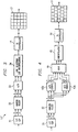
- FIGURE 1 is a block diagram of a display system having a secondary image data converter in accordance with the invention.
- FIGURE 2 is a block diagram of one embodiment of the secondary image data converter of FIGURE 1, with a display device having a staggered pixel array.
- FIGUREs 2A and 2B illustrate the even-line and odd-line patterns selected by the multiplexer of FIGURE 2.
- FIGUREs 2C and 2D illustrate 1:9 line selection by the multiplexer of FIGURE 2 for non-proscan and proscan data, respectively.
- FIGURE 3 is a block diagram of another embodiment of the secondary image data converter of FIGURE 1, used for progressive scan displays.
- FIGURE 4 is a block diagram of another embodiment of the secondary image data converter of FIGURE 1, used for progressive scan displays on a display device having a staggered pixel array.
- FIGURE 4A illustrates an interpolation scheme implemented by the secondary image data converter of FIGURE 4.
- the following description is in terms of a video display system that uses a spatial light modulator (SLM) rather than a cathode ray tube (CRT) to generate images.
- SLM spatial light modulator
- CRT cathode ray tube
- the various aspects of the invention could also be used with for other pixel array display devices, such as an LCD, which have individually addressed pixels rather than a scanned display.
- the progressive scan aspects of the invention could further be used with a CRT display system, or other display system that processes video data digitally before converting it back to an analog signal for display.
- FIGURE 1 is a block diagram of a display system 10, which receives an analog video signal, such as a broadcast television signal.
- an NTSC signal which is interlaced in even-row and odd-row fields, is assumed.
- the input signal has a luminance component and color difference components.
- the signal is a YUV signal, but the invention is useful with other color difference signals, such as a Y, B-Y, and R-Y signal. Only those components of display system 10 that are significant to main-screen and secondary-screen data processing are shown. Other components, such as might be used for processing synchronization and audio signals or for features such as closed captioning, are not shown.
- signal interface 11 receives an analog video signal and separates video, synchronization, and audio signals.
- signal interface 11 obtains the signal for the main image and for the secondary image.
- POP picture-outside-picture
- Signal interface 11 delivers the video signal for the main image to A/D converter 12a and Y/C separator 12b, which convert the data into pixel-data samples and which separate the luminance ("Y") data from the chrominance ("C") data, respectively.
- Y/C separator 12b also divides the chrominance data into its various components, such as U and V in this example.
- the signal is converted to digital data before Y/C separation, but in other embodiments, Y/C separation could be performed before A/D conversion.
- Signal interface 11 delivers the video signal for the secondary image to secondary image data converter 13.
- This signal may come from a second tuner for a television signal or from an input from another device such as a video camera/recorder (VCR).
- VCR video camera/recorder
- secondary image data converter 13 scales the data to the desired number of rows and pixels per row. It then delivers the secondary image data to a control unit 14, which inserts the secondary image data into the proper location with respect to the main image data.
- various embodiments of the invention provide secondary image data as pixel data that may or may not need further processing before delivery to display memory 16. Typically, all data for the final image undergoes color conversion and linearization in the same process, although the main image data and the secondary image data could undergo this processing separately.
- Processor system 15 prepares the data for display, by performing various pixel data processing tasks.
- Processor system 15 may include various memory devices for storing pixel data during processing, such as field and line buffers.
- the tasks performed by processor system 15 may include linearization, colorspace conversion, and conversion from interlace to progressive scan displays ("proscan").
- the proscan process converts interlaced fields having n odd rows or n even rows of data into display frames having 2n rows.
- the order in which these tasks are performed may vary.
- secondary image data converter 13 may provide data that is already proscanned. In this case, the secondary image would be inserted after the main image has been "proscanned.”
- Display memory 16 receives processed pixel data from processor system 15. Either processor 15 or display memory 16 formats the data into "bit-plane" format.
- the bit-plane format permits each pixel element of SLM 16 to be turned on or off in response to the value of 1 bit of data at a time.
- display memory 16 is a "double buffer” memory, which means that it has a capacity for at least two display frames. The buffer for one display frame can be read out to SLM 17 while the buffer another display frame is being written. The two buffers are controlled in a "ping-pong" manner so that data is continuously available to SLM 17.
- SLM 17 may be any type of SLM. As stated above, although this description is in terms of a DMD-type of SLM 17, other types of pixel array display devices could be substituted into display system 10 and used for the invention described herein. Details of a suitable SLM 17 are set out in U.S. Patent No. 4,956,619, entitled “Spatial Light Modulator,” which is assigned to Texas Instruments Incorporated, and incorporated by reference herein. In the example of this description, SLM 17 has a 640x480 array of mirror elements, each of which is individually addressable. When addressed, the direction in which each mirror tilts, on or off, results in a reflected image.
- Display optics unit 18 has optical components for receiving the image from SLM 17 and for illuminating an image plane such as a display screen.
- image plane such as a display screen.
- the bit-planes for each color could be sequenced and synchronized to a color wheel that is part of display optics unit 18.
- the data for different colors could be concurrently displayed on multiple SLMs and combined by display optics unit 18.
- Master timing unit 19 provides various system control functions.
- U.S. Patent No. 5,278,652, entitled “DMD Architecture and Timing for Use in a Pulse-Width Modulated Display System” describes a method of formatting video data for use with a DMD-based display system and a method of modulating bit-planes of data to provide varying pixel brightness.
- FIGURE 2 is a block diagram of a secondary image data converter 13' for providing pixel data to an SLM 17 having a staggered pixel array. As indicated, this means that the pixels of SLM 17 are offset by 1 ⁇ 2 pixel width from one line to another.
- Data converter 13' receives an analog Y/C signal representing the secondary image from signal interface 11.
- Y/C separator 21 separates the Y component of the signal from the C components, such as U and V. If, in the signal path for the main image, as illustrated in FIGURE 1, Y/C separator 12a operates on the analog signal rather than on digital data after sampling, the functions of Y/C separator 12a and Y/C separator 21 could be combined in a single unit that operates on both the main image signal and the secondary image signal.
- Analog filter 22 receives the Y, U, and V signals. Filter 22 implements such functions as anti-aliasing function and peaking. An example of a suitable filter is described in U.S. Patent No.5,459,528, referenced in the Background and incorporated by reference herein. For anti-aliasing, filter 22 filters out high frequency components of the signals. For peaking, the higher frequencies of the non-filtered part of the signals are amplified. The optimum amount and range of peaking are somewhat subjective, and may be experimentally derived.
- the filtered signals are received by A/D converter 23.
- A/D converter 23 has at least one sample rate, such as for 1:9 scaling or for 1:16 scaling.
- A/D converter 23 could have other sample rates and could be selectable between two or more sample rates, depending on which horizontal scaling factor(s) are desired to be supported.
- the desired sample rate can be varied by selecting a clock input.
- the sample rate assuming one sample per pixel, can be determined from the scaling ratio, the number of pixels per line in the main image, and the line rate. For example, for a display having a main image of 640 pixels per line, a 1:9 scaling ratio has a horizontal scaling factor of 1/3, for 213 (640/3) samples per line, plus any horizontal blanking time.
- a feature of secondary image data converter 13' is that for staggered pixels, this rate is doubled.
- A/D converter 23 runs at 2/3 or 1 ⁇ 2, respectively, of the sample rate of the main image.
- low pass filter 22 and A/D converter 23 are now represented by twice the number of samples needed per line. Also, at this point, the data represents an unscaled number of lines per field. Each even or odd field of data has the same number of lines as the main image, as determined by the horizontal sync signals.
- Multiplexer 24 receives three bit streams, one of Y data, one of U data, and one of V data. For even output rows of SLM 17, multiplexer 24 selects data from these bit streams in an "even-row" pattern. For odd output rows of SLM 17, multiplexer 24 selects data in an "odd-row” pattern. These patterns each have a Y value every other sample, separated by either a U value or a V value. As between the two patterns, the Y values are offset by one sample. This accommodates the offset of the staggered pixels from line to line.
- FIGURE 2A illustrates an example of the output of multiplexer 24, as compared to the pixel data for the main image, for 1:9 secondary images.
- the Y values are "fully sampled” in the sense that there is a Y value for every pixel of the secondary image.
- the C values, U and V, are "half sampled.”
- the Y values of even lines are offset from Y value of odd lines, so that the Y values correspond with the pixel positions in the staggered pixel array.
- multiplexer 24 switches between these patterns depending on whether the current line will become an even line or an odd line of SLM 17.
- the designation of one pattern as "even” and one as “odd” is arbitrary; the patterns could be switched for even and odd.
- FIGURE 2B illustrates an example of the output of multiplexer 24, as compared to the pixel data for the main image, for 1:16 secondary images. There is one Y value for every four values of the main image. Like the 1:9 pixel data, the Y values are fully sampled and the C values are half sampled.
- Secondary image data converter 13' may be configured to output data in interlaced or progressive scan format.
- the former configuration is used when SLM 17 is an interlaced display device or when SLM 17 is a progressive scan device and main image processor 15 performs the interlaced to progressive scan conversion on both the main image and the secondary image.
- the latter configuration is used when SLM 17 is a progressive scan device and secondary image data converter 13' performs the interlaced to progressive scan conversion on the secondary image.
- FIGURE 2C illustrates a possible line selection scheme for a 1:9 image for an even input field. All of the output lines produced from an even input field will become even lines on SLM 17, with main image processor producing the odd lines on SLM 17. Conversely, all of the output lines produced from an odd input field will become odd lines on SLM 17, with the main image processor 15 producing even lines on SLM 17. Therefore, the even and odd sampling patterns in FIGURE 2A swap field-to-field as opposed to line-to-line. For a 1:16 output image, multiplexer 24 selects one output line for every four input lines.
- FIGURE 2D illustrates a possible line selection scheme for a 1:9 image for an even input field.
- secondary image data converter 13' produces alternating even and odd lines on SLM 17, so the even and odd sampling patterns of FIGURE 2A swap line-to-line.
- multiplexer 24 selects one output line for every two input lines.
- multiplexer 24 selects the desired number of output lines. For each output line, multiplexer 24 selects the proper pattern depending on whether that line is to become an even output line or an odd output line. Once the samples are selected, the Y, U, and V samples are combined to generate pixel data for each pixel to be displayed. In FIGURE 1, this combination of Y,U, and V values is performed by processor 13, but could be performed by additional logic circuitry (not shown) in secondary image data generator 13'.
- the multiplexing could be performed on the analog YUV components before sampling.
- the A/D conversion would provide the same even-line and odd-line patterns described above.
- FIGURE 3 is a block diagram of secondary image data converter 13'' for providing progressive scan ("proscan") data to SLM 17.
- the input video signal is an interlaced signal.
- each input field of interlaced data becomes a complete frame of SLM data.
- SLM 17 may have either a staggered or non-staggered pixel array; however, a special embodiment of secondary image data converter 13 for progressive scan displays on a staggered pixel array device is described in connection with FIGURE 4.
- A/D converter 33 receives a Y signal, a U signal, and a V signal from analog filter 22.
- the sample rate is determined by the scaling ratio, the number of pixels per line in the main image, and the line rate. For example, for a display having a main image of 640 pixels per line, a 1:9 scaling ratio has a horizontal scaling factor of 1/3, for 213 (640/3) samples per line. This value, plus an appropriate number of samples for horizontal blanking time, is multiplied by the line rate (lines per second), to obtain the sample rate (samples per second).
- A/D converter 33 runs at 1/3 or 1/4, respectively, of the sample rate for the main image.
- the result of the sampling step is streams of Y and C data samples. These samples are ordered field-by-field of lines of samples. From each field of input data, line selector 34 selects the appropriate number of lines for a progressively scanned frame. In general, the number of lines selected is 2/n(v), where 1/n(v) is the vertical scaling factor. For example, for a 1:9 image, the vertical scaling factor is 1/3 and line selector 34 selects two output lines from every three input lines. This can be accomplished by de-selecting every third line. For a 1:16 image, the vertical scaling factor is 1/4 and line selector 34 selects one output line from every two input lines. In either case, because the input field was of lines of interlaced data, the output frame has the correct number of lines for a progressive scan display.
- line selector 34 includes an interpolation processor, which interpolates every three lines to generate two lines. For example, for a 1:9 image, pixel values from lines 1 and 2 of the input field might be interpolated to form line 1 of an output frame. Then, pixel value from lines 2 and 3 of the input field could be interpolated to form line 2 of the output frame. This process would continue for each line of the input field so that the output frame had 2/3 as many lines as the input field. For a 1:16 image, line selector 24 would interpolate every two adjacent input lines to create one output line.
- the Y, U, and V samples are combined to form a pixel value for each pixel to be displayed.
- data is available for fully sampled Y, U, and V values, but in alternative embodiments, A/D converter 33 could be modified to provide less than fully sampled chrominance data.
- the data is combined either by processor 13 or by additional logic (not shown) in secondary image data generator 13'' and is then ready for insertion into same data path as the main image pixel data.
- FIGURE 4 is a block diagram of secondary image data converter 13''' for interpolated pixel data for an SLM 17 having a staggered pixel array.
- Data converter 13''' is used as an alternative to data converter 13', when it is desired to interpolate the samples rather than to simply select some lines and de-select others.
- Y/C separator 21 and analog filter 22 perform the same functions as for the data converters 13' and 13'' of FIGUREs 2 and 3.
- Two A/D converters 43a and 43b each provide three streams of Y, U, and V data.
- a first A/D converter 43a provides data for even output lines in one of the patterns described above in connection with FIGUREs 2A and 2B.
- a second A/D converter 43b provides data for odd output lines in the other of the patterns described above.
- Multiplexer 44 selects data for interpolation for output lines. In general, for even output lines, multiplexer 44 selects data from one of the patterns. For odd output lines, it selects data from the other of the patterns. Interpolator 45 interpolates the selected data to generate each output line. The number of output lines per frame depends on whether or not the data is proscan data. As explained above, for non-proscan data, 1/n(v) output lines are provided, whereas for proscan data, 2/n(v) output lines are provided.
- FIGURE 4A illustrates a possible interpolation scheme for a 1:9 proscan image.
- Input lines 0 and 1 are interpolated to create output line 0.
- the output of A/D converter 43a is selected in the even-line pattern described above in connection with FIGURE 2A.
- Input lines 1 and 2 are interpolated to create output line 1.
- the output of A/D converter 43b is selected in the odd-line pattern described above in connection with FIGURE 2A.
- An alternate embodiment would combine A/D converters 43a and 43b into one A/D converter 43, operating at twice the sample clock rate. This single, faster A/D converter 43 would provide both even and odd sampling patterns directly to interpolator 45, eliminating the need for multiplexer 44.
- the need for two A/D converters 43a and 43b also depends on the scaling factor and the interpolation scheme. For some interpolation schemes, such as for a 1:16 proscan image where every two adjacent input lines are interpolated to become an output line, it is not necessary to use the same input line to generate two output lines. In this case, only one A/D converter 43 is required, eliminating the need for multiplexer 44.
Landscapes
- Engineering & Computer Science (AREA)
- Multimedia (AREA)
- Signal Processing (AREA)
- Computer Graphics (AREA)
- Television Systems (AREA)
- Color Television Systems (AREA)
- Controls And Circuits For Display Device (AREA)
- Studio Circuits (AREA)
Applications Claiming Priority (2)
| Application Number | Priority Date | Filing Date | Title |
|---|---|---|---|
| US298295P | 1995-08-30 | 1995-08-30 | |
| US2982 | 1995-08-30 |
Publications (2)
| Publication Number | Publication Date |
|---|---|
| EP0762752A2 true EP0762752A2 (de) | 1997-03-12 |
| EP0762752A3 EP0762752A3 (de) | 1997-06-04 |
Family
ID=21703498
Family Applications (1)
| Application Number | Title | Priority Date | Filing Date |
|---|---|---|---|
| EP96113833A Withdrawn EP0762752A3 (de) | 1995-08-30 | 1996-08-29 | Abtasten eines analogen Videosignals für sekundäre Bilder |
Country Status (6)
| Country | Link |
|---|---|
| EP (1) | EP0762752A3 (de) |
| JP (1) | JPH09204168A (de) |
| KR (1) | KR100426999B1 (de) |
| CN (1) | CN1149801A (de) |
| CA (1) | CA2184121A1 (de) |
| TW (1) | TW364258B (de) |
Cited By (1)
| Publication number | Priority date | Publication date | Assignee | Title |
|---|---|---|---|---|
| WO2000007366A1 (en) * | 1998-07-31 | 2000-02-10 | Thomson Licensing S.A. | Decimation of a high definition video signal |
Families Citing this family (3)
| Publication number | Priority date | Publication date | Assignee | Title |
|---|---|---|---|---|
| US8698958B2 (en) | 2010-06-16 | 2014-04-15 | Silicon Image, Inc. | Mechanism for memory reduction in picture-in-picture video generation |
| CN103024303B (zh) * | 2011-09-20 | 2016-03-30 | 比亚迪股份有限公司 | 图像像素阵列 |
| CN110519530B (zh) * | 2019-06-13 | 2021-07-16 | 眸芯科技(上海)有限公司 | 基于硬件的画中画显示方法及装置 |
Family Cites Families (7)
| Publication number | Priority date | Publication date | Assignee | Title |
|---|---|---|---|---|
| DE2542502A1 (de) * | 1975-09-24 | 1977-04-07 | Itt Ind Gmbh Deutsche | Fernsehempfaenger mit einer einrichtung zur gleichzeitigen wiedergabe mehrerer programme |
| US4665439A (en) * | 1986-06-05 | 1987-05-12 | North American Philips Consumer Electronics Corp. | Piecewise recursive vertical filter for PIP feature |
| US4782391A (en) * | 1987-08-19 | 1988-11-01 | Rca Licensing Corporation | Multiple input digital video features processor for TV signals |
| GB9012326D0 (en) * | 1990-06-01 | 1990-07-18 | Thomson Consumer Electronics | Wide screen television |
| FI87415C (fi) * | 1990-06-08 | 1992-12-28 | Telenokia Oy | Apparatur foer detektering av ett fel i en foerstaerkare som aer foerdubblad med hetberedskapsmetoden |
| KR950014577B1 (ko) * | 1992-08-25 | 1995-12-08 | 삼성전자주식회사 | 고화질 텔레비젼의 픽쳐인픽쳐신호처리방법 및 그 장치 |
| US5459528A (en) * | 1994-03-31 | 1995-10-17 | Texas Instruments Incorporated | Video signal processor and method for secondary images |
-
1996
- 1996-08-26 CA CA002184121A patent/CA2184121A1/en not_active Abandoned
- 1996-08-29 EP EP96113833A patent/EP0762752A3/de not_active Withdrawn
- 1996-08-29 JP JP8228953A patent/JPH09204168A/ja active Pending
- 1996-08-30 CN CN96113391A patent/CN1149801A/zh active Pending
- 1996-08-30 KR KR1019960036705A patent/KR100426999B1/ko not_active Expired - Lifetime
- 1996-11-08 TW TW085113632A patent/TW364258B/zh not_active IP Right Cessation
Cited By (1)
| Publication number | Priority date | Publication date | Assignee | Title |
|---|---|---|---|---|
| WO2000007366A1 (en) * | 1998-07-31 | 2000-02-10 | Thomson Licensing S.A. | Decimation of a high definition video signal |
Also Published As
| Publication number | Publication date |
|---|---|
| EP0762752A3 (de) | 1997-06-04 |
| JPH09204168A (ja) | 1997-08-05 |
| TW364258B (en) | 1999-07-11 |
| CN1149801A (zh) | 1997-05-14 |
| KR100426999B1 (ko) | 2004-07-19 |
| KR970014229A (ko) | 1997-03-29 |
| CA2184121A1 (en) | 1997-03-01 |
Similar Documents
| Publication | Publication Date | Title |
|---|---|---|
| EP0661889B1 (de) | Verfahren und Vorrichtung zur Verarbeitung von Videodaten | |
| EP0647070B1 (de) | Farbtrennungsgerät und Verfahren für digitales Fernsehen | |
| US5459528A (en) | Video signal processor and method for secondary images | |
| EP0651577B1 (de) | Digitales Fernsehsystem | |
| US5530482A (en) | Pixel data processing for spatial light modulator having staggered pixels | |
| US5838385A (en) | Sampling analog video signal for secondary images | |
| US5671018A (en) | Motion adaptive vertical scaling for interlaced digital image data | |
| JP3953561B2 (ja) | 画像信号のフォーマット変換信号処理方法及び回路 | |
| JP3354927B2 (ja) | 表示システム | |
| CA1230669A (en) | Progressive scan television display system | |
| US6040869A (en) | Method and apparatus for converting an interlace-scan video signal into a non-interlace-scan video signal | |
| KR100332329B1 (ko) | 영상신호변환장치 | |
| US5587744A (en) | Image display apparatus | |
| EP0762752A2 (de) | Abtasten eines analogen Videosignals für sekundäre Bilder | |
| JPH10513015A (ja) | レターボックスの表示制御 | |
| JP2005192230A (ja) | 表示装置 | |
| JP2642464B2 (ja) | テレビジョン信号変換装置 | |
| KR100253001B1 (ko) | 100 헤르츠 티브이 | |
| JPH04345389A (ja) | ワイドアスペクト変換機能付ワイド画面テレビジョン受信機 | |
| KR100209849B1 (ko) | 와이드 스크린 텔레비젼용 수평 패닝 장치 | |
| JPH0394595A (ja) | 映像信号変換装置 | |
| JPH10191197A (ja) | テレビジョン受信機 | |
| JP2002359819A (ja) | 順次走査変換回路、セットトップボックス、テレビジョン受像機、及び順次走査変換方法 | |
| JPH0346492A (ja) | 映像信号変換装置 | |
| JP2000004424A (ja) | 映像信号処理方法及び装置 |
Legal Events
| Date | Code | Title | Description |
|---|---|---|---|
| PUAI | Public reference made under article 153(3) epc to a published international application that has entered the european phase |
Free format text: ORIGINAL CODE: 0009012 |
|
| AK | Designated contracting states |
Kind code of ref document: A2 Designated state(s): DE FR GB IT NL |
|
| PUAL | Search report despatched |
Free format text: ORIGINAL CODE: 0009013 |
|
| AK | Designated contracting states |
Kind code of ref document: A3 Designated state(s): DE FR GB IT NL |
|
| 17P | Request for examination filed |
Effective date: 19970729 |
|
| 17Q | First examination report despatched |
Effective date: 19990716 |
|
| STAA | Information on the status of an ep patent application or granted ep patent |
Free format text: STATUS: THE APPLICATION IS DEEMED TO BE WITHDRAWN |
|
| 18D | Application deemed to be withdrawn |
Effective date: 20010807 |