EP0765022A2 - Unterbrechungsfreies Schaltreglersystem - Google Patents
Unterbrechungsfreies Schaltreglersystem Download PDFInfo
- Publication number
- EP0765022A2 EP0765022A2 EP96102272A EP96102272A EP0765022A2 EP 0765022 A2 EP0765022 A2 EP 0765022A2 EP 96102272 A EP96102272 A EP 96102272A EP 96102272 A EP96102272 A EP 96102272A EP 0765022 A2 EP0765022 A2 EP 0765022A2
- Authority
- EP
- European Patent Office
- Prior art keywords
- circuit
- voltage
- winding
- tertiary
- switching
- Prior art date
- Legal status (The legal status is an assumption and is not a legal conclusion. Google has not performed a legal analysis and makes no representation as to the accuracy of the status listed.)
- Granted
Links
Images


Classifications
-
- H—ELECTRICITY
- H02—GENERATION; CONVERSION OR DISTRIBUTION OF ELECTRIC POWER
- H02M—APPARATUS FOR CONVERSION BETWEEN AC AND AC, BETWEEN AC AND DC, OR BETWEEN DC AND DC, AND FOR USE WITH MAINS OR SIMILAR POWER SUPPLY SYSTEMS; CONVERSION OF DC OR AC INPUT POWER INTO SURGE OUTPUT POWER; CONTROL OR REGULATION THEREOF
- H02M1/00—Details of apparatus for conversion
- H02M1/42—Circuits or arrangements for compensating for or adjusting power factor in converters or inverters
- H02M1/4208—Arrangements for improving power factor of AC input
- H02M1/4258—Arrangements for improving power factor of AC input using a single converter stage both for correction of AC input power factor and generation of a regulated and galvanically isolated DC output voltage
-
- H—ELECTRICITY
- H02—GENERATION; CONVERSION OR DISTRIBUTION OF ELECTRIC POWER
- H02J—ELECTRIC POWER NETWORKS; CIRCUIT ARRANGEMENTS OR SYSTEMS FOR SUPPLYING OR DISTRIBUTING ELECTRIC POWER; SYSTEMS FOR STORING ELECTRIC ENERGY
- H02J9/00—Circuit arrangements for emergency or stand-by power supply, e.g. for emergency lighting
- H02J9/04—Circuit arrangements for emergency or stand-by power supply, e.g. for emergency lighting in which the distribution system is disconnected from the normal source and connected to a standby source
- H02J9/06—Circuit arrangements for emergency or stand-by power supply, e.g. for emergency lighting in which the distribution system is disconnected from the normal source and connected to a standby source with automatic change-over, e.g. UPS systems
- H02J9/061—Circuit arrangements for emergency or stand-by power supply, e.g. for emergency lighting in which the distribution system is disconnected from the normal source and connected to a standby source with automatic change-over, e.g. UPS systems for DC powered loads
-
- H—ELECTRICITY
- H02—GENERATION; CONVERSION OR DISTRIBUTION OF ELECTRIC POWER
- H02M—APPARATUS FOR CONVERSION BETWEEN AC AND AC, BETWEEN AC AND DC, OR BETWEEN DC AND DC, AND FOR USE WITH MAINS OR SIMILAR POWER SUPPLY SYSTEMS; CONVERSION OF DC OR AC INPUT POWER INTO SURGE OUTPUT POWER; CONTROL OR REGULATION THEREOF
- H02M3/00—Conversion of DC power input into DC power output
- H02M3/22—Conversion of DC power input into DC power output with intermediate conversion into AC
- H02M3/24—Conversion of DC power input into DC power output with intermediate conversion into AC by static converters
- H02M3/28—Conversion of DC power input into DC power output with intermediate conversion into AC by static converters using discharge tubes with control electrode or semiconductor devices with control electrode to produce the intermediate AC
- H02M3/325—Conversion of DC power input into DC power output with intermediate conversion into AC by static converters using discharge tubes with control electrode or semiconductor devices with control electrode to produce the intermediate AC using devices of a triode or a transistor type requiring continuous application of a control signal
- H02M3/335—Conversion of DC power input into DC power output with intermediate conversion into AC by static converters using discharge tubes with control electrode or semiconductor devices with control electrode to produce the intermediate AC using devices of a triode or a transistor type requiring continuous application of a control signal using semiconductor devices only
-
- H—ELECTRICITY
- H02—GENERATION; CONVERSION OR DISTRIBUTION OF ELECTRIC POWER
- H02M—APPARATUS FOR CONVERSION BETWEEN AC AND AC, BETWEEN AC AND DC, OR BETWEEN DC AND DC, AND FOR USE WITH MAINS OR SIMILAR POWER SUPPLY SYSTEMS; CONVERSION OF DC OR AC INPUT POWER INTO SURGE OUTPUT POWER; CONTROL OR REGULATION THEREOF
- H02M3/00—Conversion of DC power input into DC power output
- H02M3/22—Conversion of DC power input into DC power output with intermediate conversion into AC
- H02M3/24—Conversion of DC power input into DC power output with intermediate conversion into AC by static converters
- H02M3/28—Conversion of DC power input into DC power output with intermediate conversion into AC by static converters using discharge tubes with control electrode or semiconductor devices with control electrode to produce the intermediate AC
- H02M3/325—Conversion of DC power input into DC power output with intermediate conversion into AC by static converters using discharge tubes with control electrode or semiconductor devices with control electrode to produce the intermediate AC using devices of a triode or a transistor type requiring continuous application of a control signal
- H02M3/335—Conversion of DC power input into DC power output with intermediate conversion into AC by static converters using discharge tubes with control electrode or semiconductor devices with control electrode to produce the intermediate AC using devices of a triode or a transistor type requiring continuous application of a control signal using semiconductor devices only
- H02M3/33569—Conversion of DC power input into DC power output with intermediate conversion into AC by static converters using discharge tubes with control electrode or semiconductor devices with control electrode to produce the intermediate AC using devices of a triode or a transistor type requiring continuous application of a control signal using semiconductor devices only having several active switching elements
-
- H—ELECTRICITY
- H02—GENERATION; CONVERSION OR DISTRIBUTION OF ELECTRIC POWER
- H02J—ELECTRIC POWER NETWORKS; CIRCUIT ARRANGEMENTS OR SYSTEMS FOR SUPPLYING OR DISTRIBUTING ELECTRIC POWER; SYSTEMS FOR STORING ELECTRIC ENERGY
- H02J9/00—Circuit arrangements for emergency or stand-by power supply, e.g. for emergency lighting
- H02J9/04—Circuit arrangements for emergency or stand-by power supply, e.g. for emergency lighting in which the distribution system is disconnected from the normal source and connected to a standby source
- H02J9/06—Circuit arrangements for emergency or stand-by power supply, e.g. for emergency lighting in which the distribution system is disconnected from the normal source and connected to a standby source with automatic change-over, e.g. UPS systems
- H02J9/067—Circuit arrangements for emergency or stand-by power supply, e.g. for emergency lighting in which the distribution system is disconnected from the normal source and connected to a standby source with automatic change-over, e.g. UPS systems using multi-primary transformers, e.g. transformer having one primary for each AC energy source and a secondary for the loads
-
- Y—GENERAL TAGGING OF NEW TECHNOLOGICAL DEVELOPMENTS; GENERAL TAGGING OF CROSS-SECTIONAL TECHNOLOGIES SPANNING OVER SEVERAL SECTIONS OF THE IPC; TECHNICAL SUBJECTS COVERED BY FORMER USPC CROSS-REFERENCE ART COLLECTIONS [XRACs] AND DIGESTS
- Y02—TECHNOLOGIES OR APPLICATIONS FOR MITIGATION OR ADAPTATION AGAINST CLIMATE CHANGE
- Y02B—CLIMATE CHANGE MITIGATION TECHNOLOGIES RELATED TO BUILDINGS, e.g. HOUSING, HOUSE APPLIANCES OR RELATED END-USER APPLICATIONS
- Y02B70/00—Technologies for an efficient end-user side electric power management and consumption
- Y02B70/10—Technologies improving the efficiency by using switched-mode power supplies [SMPS], i.e. efficient power electronics conversion e.g. power factor correction or reduction of losses in power supplies or efficient standby modes
Definitions
- the present invention relates to an uninterruptive switching regulator which has a high power factor and is reduced in a higher harmonic component in a primary-side a.c. input current as well as an output ripple, and more particularly to a technique for realizing an uninterruptive switching regulator of the self-excitation type which is reduced in the number of parts, downsized and inexpensive.
- a primary side circuit 110 in which a primary winding 106 of a high-frequency transformer 104 and a primary side switching element 108 are connected in series to an output side of the rectifier circuit 102, to develop a primary side high frequency pulse voltage through the primary side switching element 108;
- a secondary side circuit 116 in which a rectifying and smoothing circuit is connected to a secondary winding 112 of the above high-frequency transformer 104, to supply a d.c.
- a charge circuit 126 in which an electrical double layer capacitor 120, a choke coil 122 and a high-frequency rectifier diode 124 are connected in series to a tertiary winding 118 of the above high-frequency transformer 104; (5) a discharge circuit 132 in which the above electrical double layer capacitor 120 and a tertiary side switching element 130 are connected in series between a winding start portion of the above tertiary winding 118 and a winding end portion thereof or a tap 128 drawn out from the middle portion of that winding; and (6) a pulse width modulation control switching control circuit 134 which outputs a pulse signal in synchronism with the above primary side switching element 108 and the tertiary side switching element 130 to perform a switching operation and also modulates the pulse width of a pulse signal in response to the fluctuation of an output voltage of the above secondary side circuit 116 to control the pulse width of the primary side high-frequency pulse voltage.
- the conventional uninterruptive switching regulator like this operates as follows: When the output voltage of the rectifier circuit 102 exceeds a predetermined level, a sine-wave alternating current supplied from the a.c. power supply 100 is supplied to the primary side of the high-frequency transformer 104 in the form of a full-wave sine-wave pulsating current waveform. Then, the full-wave sine-wave pulsating current flows in the primary side switching element 108 through the primary winding 106 and a reverse current preventing diode 136, and is chopped while being controlled by the switching control circuit 134, then being outputted to the secondary side circuit 116.
- a current i 1 which flows in the primary side circuit 110 when the primary side switching element 108 is on, causes a current i 2 shown in the figure to flow in a tertiary side circuit 138.
- the current i 2 is smoothed by the choke coil 122 and charges the electrical double layer capacitor 120.
- the discharge current i 3 flows through a winding portion between the winding start portion of the tertiary winding 118 and the halfway tap 128.
- the discharge current i 3 is chopped by the tertiary side switching element 130 and outputted to the secondary side circuit 116.
- the conventional uninterruptive switching regulator suffers from such a problem that its separate excitation type makes it difficult to downsize the device and to lower the costs.
- the pulse width modulation control circuit (PWM) 134 is used for the purpose of obtaining the primary side pulse voltage, which is a basic part separately controlled and separately attached.
- the requirement of such a basic part which is separately controlled and separately attached causes not only an increase in the number of parts but also an increase in the costs, which is not preferred.
- the present invention has been made to solve the above-mentioned problems, and therefore an object of the invention is to provide an uninterrupted switching regulator of the self-excitation type which is capable of reducing the costs and being downsized.
- an uninterrupted switching regulator which comprises a rectifier circuit for rectifying an alternating current from an a.c. power supply; a primary side circuit for developing a primary side high frequency pulse voltage through a primary side switching element in which a primary winding of a high-frequency transformer and the primary side switching element are connected in series to an output side of the rectifier circuit, and a switching primary winding for applying a switching control voltage to the primary side switching element is connected to the output side of the rectifier circuit; a secondary side circuit for applying a d.c.
- a rectifying and smoothing circuit is connected to a secondary winding of said high-frequency transformer; a charge circuit connected in series to a first tertiary winding of the high-frequency transformer and including an electrical double layer capacitor or a secondary battery and a rectifying device; and a discharge circuit in which a second tertiary winding connected in series to said first tertiary winding, a tertiary side switching element and said electrical double layer capacitor or secondary battery are connected in series to each other, and a switching tertiary winding for applying a switching control voltage to the tertiary side switching element is connected thereto, for developing a primary side high-frequency pulse discharge voltage from the discharge output of the electrical double layer capacitor or the secondary battery through said tertiary side switching element, in which an output is transmitted from the primary side and the tertiary side to the secondary side through the flyback system, and said charge circuit operates when the output voltage of said rectifier circuit at the primary side exceeds a predetermined level
- the output transformer of one switching circuit of the RCC (ringing choke converter) system which inputs a commercial a.c. is common in the magnetic path of an iron core to the output transformer of the other switching circuit of the RCC system using the charged energy stored in the electrical double layer capacitor or the secondary battery as an input source.
- the switching operation (a timing of turning on/off) of the primary side switching element completely synchronizes with that of the tertiary side switching element, and the higher potential of the commercial a.c. or the d.c. input of the electrical double layer capacitor or secondary battery is automatically preferentially effected by self-exciting operation, resulting in the uninterruptive switching regulator.
- the output supply from the RCC circuit at the commercial a.c. side is usually preferentially effected.
- the electrical double layer capacitor or the secondary battery is charged with a constant voltage or constant current directly or through a regulator or the like by an electromotive voltage induced in the tertiary winding, for an unexpected situation such as a power failure.
- the RCC circuit at the commercial a.c. side is automatically switched to the RCC circuit using the energy from the electrical double layer capacitor or secondary battery which have been charged as an input source, to thereby supply an output from the first tertiary winding.
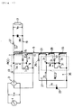
- Fig. 1 is a diagram for explaining the principle of the present invention, in which parts other than main parts for explanation are omitted therefrom.
- Shown in the figure is a basic circuit of an uninterruptive switching regulator which comprises: a rectifier circuit 3 for rectifying an alternating current from an a.c. power supply 1; a primary side circuit 13 for developing a primary side high frequency pulse voltage through a primary side switching element 9 in which a primary winding 7 of a high-frequency transformer 5 and the primary side switching element 9 are connected in series to an output side of the rectifier circuit 3, and a switching primary winding 11 for applying a switching control voltage to the primary side switching element 9 is connected to the output side of the rectifier circuit 3; a secondary side circuit 19 for applying a d.c.
- a rectifying and smoothing circuit is connected to a secondary winding 15 of said high-frequen cy transformer 5; a charge circuit 27 connected in series to a first tertiary winding 21 of the high-frequency transformer 5 and including an electrical double layer capacitor 23 or a secondary battery 23 and a rectifying device 25; and a discharge circuit 35 in which a second tertiary winding 29 connected in series to said first tertiary winding 21, a tertiary side switching element 31 and said electrical double layer capacitor 23 or secondary battery 23 are connected in series to each other, and a switching tertiary winding 33 for applying a switching control voltage to the tertiary side switching element 31 is connected thereto, for developing a primary side high-frequency pulse discharge voltage from the discharge output of the electrical double layer capacitor 23 or the secondary battery 23 through said tertiary side switching element 31; wherein an output is transmitted from the primary side and the tertiary side to the secondary side through the flyback system,
- a full-wave sine-wave pulsating current obtained by the rectifier circuit 3 flows as a base current I 1S of the primary side switching element 9 (transistor 9), and the primary side switching element 9 turns on.
- the output voltage of the rectifier circuit 3 is applied to the primary winding 7 in the high-frequency transformer 5, which makes a current I 1 flow.
- an induced voltage E A corresponding to the respective turn ratios is developed in the switching primary winding 11, thereby allowing a current I 2 which forms a base current to flow.
- the counter-electromotive force is developed in the respective wirings of the high-frequency transformer 5, whereby the magnetic energy stored in the iron core of the transformer from the secondary winding 15 through the diode 37 flows out as a charge current I c' to the smoothing capacitor 39 through the flyback system. Then, the charge current I c' makes the smoothing capacitor 39 charged, and is smoothed before being taken out as an output voltage V 0 from the secondary side circuit 19. Thereafter, the charge current I c' becomes zero after a certain period of time elapsed, and a voltage applied from the switching primary winding 11 to the base of the switching element 9 as a reverse voltage disappears.
- the primary side switching element 9 is again turned on by a current I 1S , and the switching operation is continued by the same operation as that described above.
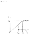
- the frequency of the switching operation is determined by the rising rate of the collector current i c shown in Fig. 2, but this is set to an appropriate value by the design of circuit constants.
- the charge current I 3 and a current I 3S which forms the base current of the tertiary side switching element 31 (transistor 31) flow so that the tertiary side switching element 31 becomes in the on-state.
- a voltage induced in the second tertiary winding 29 is reverse to a direction in which the current I 3 flows, no collector current I 4 of the tertiary side switching element 31 flows, as a result of which the tertiary side switching element 31 becomes in a no-load running state.
- the electrical double layer capacitor 23 is finally charged by the charge current I c caused by the electromotive voltage induced in the first tertiary winding 21.
- the tertiary side switching element 31 repeats the switching operation by the base current I 3S and I 5 with the same operation as that of the primary side switching element 9 in the above-mentioned primary side circuit 13, and the discharge current I D from the electrical double layer capacitor 23 is chopped by the tertiary side switching element 31 and then outputted to the secondary side circuit 19.
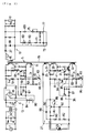
- Fig. 3 is a circuit diagram explanatorily showing an example of a circuit of the uninterruptive switching regulator in accordance with the present invention.
- a description will be given in more detail on the basis of Fig. 3.
- a rectifying device 45 is connected to an a.c. power supply 1 through a line filter 43 to constitute a rectifier circuit 3.
- a capacitor 47 functions as a filter for filtering a noise which is generated at the time of the switching operation.
- a primary winding 7 of a high-frequency transformer 5 and a primary side switching element 9 (transistor 9) are connected in series to each other through a diode 49.
- a switching primary winding 11 which applies a control voltage is connected to the switching terminal of the primary side switching element 9, that is, the base of the transistor 9 in the figure. The polarity of the switching primary winding 11 is set as shown in the figure.
- the output side of the rectifier circuit 3 and the base of the transistor 9 are connected to each other through a resistor 51 so that a base current I 1S for turning on the transistor 9 flows.
- the winding start of the switching primary winding 11 and the base of the transistor 9 are connected to each other through a d.c. component cut capacitor 53 and a resistor 55, and a resistor 57 for base voltage adjustment is connected between the winding end of the switching primary winding 11 and the base of the transistor 9.
- the collector of a transistor 59 for bypassing the base current of the transistor 9 is connected between the winding end of the switching primary winding 11 and a node between the resistor 51 and the base of the transistor 9.
- the base of the transistor 59 is connected to the winding start of the switching primary winding 11 through a diode 61 and a photo-coupler 63 to constitute a constant-voltage control circuit 65.
- a resistor 67 connected to the emitter of the transistor 59 is provided for an over-current detection of a current flowing in the primary winding 7 as the emitter current of the transistor 9.
- a primary side circuit 13 for generating a primary side high-frequency pulse voltage is formed.
- an FET may be used for the transistor 9 instead of a bipolar transistor.
- a secondary side circuit 19 to which a rectifying and smoothing circuit comprised of the diode 37 and the smoothing capacitor 39 is connected, to thereby supply a d.c. output power to the load 17.
- a photo-diode of photo-couplers 63 and 93 is provided for comparing a voltage which has been divided into a voltage detection voltage-divided resistor 69, a variable resistor 75 and a detection resistor 77 with the internal reference voltage of a comparative amplifying IC 73 which is called "a shunt regulator" to perform a constant-voltage control.
- a first tertiary winding 21 which is wound in the same direction as that of the primary winding 7 is disposed on an iron core 79 which is common to that of the primary winding 7.
- the rectifying diode 25, the constant-voltage constant-current control transistor 80, and the electrical double layer capacitor 23 are connected in series to each other, to thereby form a charge circuit 27.
- a secondary battery may be used instead of the electrical double layer capacitor 23.
- the second tertiary winding 29 is connected to the above first tertiary winding 21 so as to have the same polarity.
- the second tertiary winding 29 and the tertiary side switching element 31 are connected in series through the diode 41, and the switching tertiary winding 33 is connected to the switching terminal of the tertiary side switching element 31, in the figure, the base of the transistor 31 so as to apply a control voltage thereto.
- the switching tertiary winding 33 is reverse in polarity to the above two tertiary windings 21 and 29.
- the plus side of the electrical double layer capacitor 23 and the base of the transistor 31 are connected to each other through a resistor 81 in such a manner that the base current I 3S for turning on the transistor 31 flows therein.
- the winding start portion of the switching tertiary winding 33 and the base of the transistor 31 are connected to each other through a d.c. component cut capacitor 83 and a resistor 85 whereas a base voltage adjustment resistor 87 is connected between the winding end portion of the switching tertiary winding 33 and the base of the transistor 31.
- a transistor 89 for allowing the base current of the transistor 31 to be bypassed is disposed between a node between the resistor 81 and the base of the transistor 31 and the winding end portion of the switching tertiary winding 33.
- the base of the transistor 89 is connected to the winding start portion of the switching tertiary winding 33 through a diode 91 and the photo-coupler 93, to thereby constitute a constant-voltage control circuit 95.
- a resistor 97 connected to the emitter of the transistor 89 is so designed as to detect an over-current of the emitter current of the transistor 31, which flows in the second tertiary winding 29.
- the discharge circuit 35 is constituted as described above.
- the transistor 9 since the above voltage E A is applied to a polarity by which the transistor 9 turns on, the transistor 9 is held in the on-state. The base voltage at this time is adjusted to an appropriate value by the resistor 57. Then, as was already described with reference to Fig. 2, since the collector current i c of the transistor 9 increases linearly, when it comes to a product of the current amplification factor h FE and the base current after a certain period of time elapsed, the collector current ceases to increase, and there is no change in the current. As a result, the direction of the electromotive force of the respective windings is reversed in such a manner that the induced voltage E A of the switching primary winding 11 becomes a reversed voltage. As a result, the transistor 9 turns off rapidly.
- the magnetic energy stored in the iron core 79 is developed as a counter-electromotive power in the respective windings of the high-frequency transformer 5, the charge current I c' of the smoothing capacitor 39 flows out from the secondary winding 15 through the diode 37. Then, the charge current I c' makes the smoothing capacitor 39 charged, and is smoothed before being taken out as the output voltage V 0 from the secondary side circuit 19. Thereafter, since the charge current I c' becomes zero after a certain period of time elapsed, because of the discharge of the magnetic energy.
- the divided voltage of the secondary side constant-voltage control detection resistor 77 becomes higher than the gate voltage of a shunted regulator 73 so that the luminance of an emitter diode in the photo-coupler 63 (and 93) is enhanced, and the emitter current of a photo-transistor in the photo-coupler 63 (and 93) positioned at the primary side is increased. Also, the base current of the transistor 59 flows through the diode 61 and the photo-coupler 63 with the forward voltage of the switching primary winding 11 as a voltage source, to thereby make the base potential of the transistor 59 rise.
- the operation timing of the transistor 59 is made fast.
- the base voltage of the transistor 9 is lowered so that a period t ON is shortened as shown in Fig. 2 whereas a period t OFF is lengthened.
- the PWM operation is conducted in such a manner that the output voltage V 0 is held a predetermined constant voltage.
- the period t ON is lengthened inversely, and the PWM operation is conducted so that the output voltage V 0 becomes the predetermined constant voltage.
- the first tertiary winding 21 has the same polarity as that of the primary winding 7, when the current I 1 flows in the primary winding 7, that is, when the transistor 9 is on, an electromotive force is generated in a direction in which no current flows by the diode 25.
- the second tertiary winding 29 also has the same winding direction as that of the primary winding 7, and therefore even in this case, the diode 41 makes no current flow.
- the switching tertiary winding 33 is opposite in winding direction to the primary winding 7, the transistor 31 turns on. However, because the potential of the second tertiary winding 29 is higher than the potential of the electrical double layer capacitor 23, no current I 4 flows.
- the electromotive forces generated in the first tertiary winding 21, the second tertiary winding 29 and the switching tertiary winding 33, respectively, are reversed, with the result that the charge current I 3 flows as the charge current (I c ) of the electrical double layer capacitor 23 while being limited by the transistor 80 which operates as a dropper, to thereby conduct the charging operation.
- the electrical double layer capacitor 23 is charged up to a constant voltage level which is determined by the shunted regulator 82.
- the base of the transistor 31 becomes a reverse bias because the electromotive force of the switching tertiary winding 33 is reverse in direction, to thereby turn off in synchronism with the transistor 9.
- the RCC circuit at the rectifier circuit 3 side (commercial a.c. input side) and the RCC circuit at the electrical double layer capacitor 23 side operate in complete synchronism with each other.
- the discharge current I 4 flowing in the second tertiary winding 29 allows an induced voltage to be developed in the switching tertiary winding 33, and the current I 5 which allows the transistor 31 to be held in the on-state flows through the capacitor 83 and the resistor 85, to thereby deeply bias the base of the transistor 31.
- the switching operation is repeated in the same manner as the operation of the transistor 9 in the above-mentioned primary side circuit 13, and the discharge current I D from the electrical double layer capacitor 23 is chopped by means of the transistor 31 and outputted to the secondary side circuit 19 to thereby exhibit the uninterruptive property.
- the shunted regulator 73 operates in the on-direction so that the current of the emitter diode in the photo-coupler 93 increases.
- the emitter current of the photo-resistor in the photo-coupler 93 flows through the diode 91 and the photo-transistor of the photo-coupler 93 with the forward voltage of the switching tertiary winding 33 as a source, which causes the base voltage of the transistor 89 to rise.
- the operation timing of the transistor 89 is made fast so that the period t ON of the transistor 31 is shortened whereas the period t OFF is lengthened. For that reason, the magnetic energy stored in the iron core 79 is reduced, and the PWM control operation is conducted in such a manner that the output voltage of the secondary side circuit 19 becomes a predetermined constant voltage.
- the regulator for the electrical double layer capacitor 23 is comprised of the transistor 80, the shunted regulator 82 and the photo-coupler 86.
- the diode 88 acts as a bypass diode only when discharging
- the resistors 90 and 92 are a partial-potential resistor for detection of a charge voltage to the electrical double layer capacitor 23 and a detection resistor, respectively.
- the sine-wave a.c. applied from the a.c. power supply 1 is rectified by the rectifying device 45 into a full-wave sine-wave pulsating current waveform shown in Fig. 4A and supplied to the primary side of the high-frequency transformer 5. In this situation, it is converted into a high-frequency pulse voltage through the switching operation of the transistor 9 and outputted to the secondary side circuit 19 by the flyback system. Since the chopping frequency at this time is determined by the collector current, current amplification factor and base current of the transistor 9 as shown in Fig. 2, it is actually set by circuit constants. In the present invention, the RCC 1 arranged at the a.c.
- the number of turns of the primary winding 7 is N 1
- the number of turns of the second tertiary winding 29 is N 3
- the input voltage of the RCC1 is V A1
- the input voltage of the RCC2 is V B1
- the specific voltage at the primary winding 7 side is V A1 /N 1
- the specific voltage at the second tertiary winding 29 side is V B1 /N 3 , respectively, and an output energy is supplied to the secondary side circuit 19 from the higher specific voltage.
- a mean voltage level for charging the electrical double layer capacitor 23 from the first tertiary winding 21 is made constant similarly to the output voltage of the secondary side circuit 19 up to a voltage level at which the constant-voltage energy can be supplied to an output as a result of the pulse width modulation switching operation at the side of the RCC1. Therefore, the RCC 2 side cannot constitute the energy supply source to the secondary side circuit 19. In this situation, the RCC 2 side is in a no-load running state, and the first tertiary winding 21 functions as a charge circuit for the electrical double layer capacitor 23.
- a slice level (indicated by S in the figure).
- a voltage higher than that slice level is actually detected by the Zener diode 84, and the regulator transistor 80 of the charge circuit may be interrupted as described above.
- the charge and discharge circuits 27 and 35 do not exist at the tertiary side. Then, the output voltage V 0 of the secondary side circuit 19 appears in the form of a square voltage waveform which is synchronous with the frequency of the a.c. power supply shown in Fig. 4B. However, when the voltage of the full-wave sine-wave pulsating current shown in Fig. 4A is not higher than a slice level S, the charge voltage of the electrical double layer capacitor 23 becomes higher than the induced voltage of the first tertiary winding 21 as described above.
- the output voltage V 0 of the secondary side circuit 19 at this time has a waveform shown in Fig. 4C, and appears in the form of a waveform which makes up the gap portions of the voltage waveform in a region where the voltage is higher than the slice level S of the full-wave sine-wave pulsating current shown in Fig. 4B.
- the flat output voltage V 0 which has no concave over all time regions is outputted from the secondary side circuit 19.
- the switching regulator of the present invention supplies the discharge power from the electrical double layer capacitor in a region where the input voltage is not higher than the slice level, an extremely enhanced power factor can be realized. It is needless to say that even in the case of a momentary power failure, the output voltage V 0 of a waveform shown in Fig. 4D is obtained by the like operation.
- the current waveform viewed from the a.c. input side was a waveform where a large current is concentrated for an extremely short period of time as indicated by reference mark A in the figure in the conventional switching regulator having the smoothing capacitor, but is a relatively flat current waveform as indicated by reference mark B in the figure in the switching regulator in accordance with the present invention.
- reference mark A in the figure in the conventional switching regulator having the smoothing capacitor
- reference mark B in the figure in the switching regulator in accordance with the present invention.
- an electrolytic capacitor 94 is disposed, and its charge voltage is set slightly higher than the electrical double layer capacitor 23 so that the supply of an energy lower than the slice level in a stationary running operation is conducted by the electrolytic capacitor 94, and at the time of a power failure, etc., after the discharge from the electrolytic capacitor 94 for an extremely short period of time has been finished, an energy may be supplied from the electrical double layer capacitor 23. With such an operation, a load on the electrical double layer capacitor 23 is reduced.
- a solar cell panel is connected to the electrical double layer capacitor 23 as a backup power supply at the time of a power failure, or RCC circuits such as RCCs 3, 4, ... are added thereto, and a diesel generator, a wind power generator, etc., are connected to the respective RCC circuits so as to provide an uninterruptive power supply (energy best mix) using a total energy.
- the output supply from the RCC circuit at the commercial a.c. side is usually preferentially effected.
- the electrical double layer capacitor or the secondary battery is charged with a constant voltage or constant current directly or through a regulator or the like by an electromotive voltage induced in the tertiary winding, for an unexpected situation such as a power failure.
- the RCC circuit at the commercial a.c. side is automatically switched to the RCC circuit using the energy from the electrical double layer capacitor or secondary battery which have been charged as an input source, to thereby supply an output from the second tertiary winding. Accordingly, an excellent uninterruptive property can be ensured with an extremely simple circuit.
- a d.c. power is supplied to a load by an output from the rectifier circuit.
- a charge is discharged from the electrical double layer capacitor through the discharge circuit connected to the iron core common to the primary side circuit, and the d.c. power is supplied to the load by the discharge power. Accordingly, even in the case of the power failure, in the region where the voltage is not higher than the slice level in the a.c.
- the electrical double layer capacitor enables rapid charge and discharge operation, and also its capacitance is remarkably large to the degree of farad unit. Therefore, the electrical double layer capacitor is excellent in a long-period reliability, and even at the time of a momentary power failure of a minute unit, a sufficient power can be supplied to the secondary side circuit. Furthermore, because the switching is of the self-excitation type, an additional main part such as a PWM as in the conventional switching regulator is not required, which can greatly contribute to a reduction in the costs of the equipment and downsizing of the equipment.
- a plurality of RCC circuits are connected to the iron core of one transformer, and an energy is applied to the secondary side circuit through any RCC circuit. Accordingly, even in any cases other than this embodiment described above, an energy can be applied from a natural energy such as a solar light generation or a wind power, a general-purpose diesel generator or the like, and a variety of energy can be totally used as a backup power supply at the time of the power failure, which extremely enhances the reliability.
- the electrical double layer capacitor or the secondary battery functions as the smoothing capacitor in the conventional rectifier circuit, this makes it unnecessary to use the smoothing capacitor at the primary side circuit.
- no choke coil to be conventionally provided in the secondary side circuit is required. This contributes to a reduction in the costs, the downsizing, and an improvement in the power factor, and provides a switching power supply with a high performance which did not exist up to now.
Landscapes
- Engineering & Computer Science (AREA)
- Power Engineering (AREA)
- Business, Economics & Management (AREA)
- Emergency Management (AREA)
- Dc-Dc Converters (AREA)
- Stand-By Power Supply Arrangements (AREA)
- Charge And Discharge Circuits For Batteries Or The Like (AREA)
- Continuous-Control Power Sources That Use Transistors (AREA)
Applications Claiming Priority (3)
| Application Number | Priority Date | Filing Date | Title |
|---|---|---|---|
| JP7244986A JP2917871B2 (ja) | 1995-09-22 | 1995-09-22 | 無停電性スイッチングレギュレータ |
| JP24498695 | 1995-09-22 | ||
| JP244986/95 | 1995-09-22 |
Publications (3)
| Publication Number | Publication Date |
|---|---|
| EP0765022A2 true EP0765022A2 (de) | 1997-03-26 |
| EP0765022A3 EP0765022A3 (de) | 1999-06-02 |
| EP0765022B1 EP0765022B1 (de) | 2004-05-12 |
Family
ID=17126889
Family Applications (1)
| Application Number | Title | Priority Date | Filing Date |
|---|---|---|---|
| EP96102272A Expired - Lifetime EP0765022B1 (de) | 1995-09-22 | 1996-02-15 | Unterbrechungsfreies Schaltreglersystem |
Country Status (5)
| Country | Link |
|---|---|
| US (1) | US5602726A (de) |
| EP (1) | EP0765022B1 (de) |
| JP (1) | JP2917871B2 (de) |
| CN (1) | CN1085354C (de) |
| DE (1) | DE69632439T2 (de) |
Cited By (1)
| Publication number | Priority date | Publication date | Assignee | Title |
|---|---|---|---|---|
| DE10245626A1 (de) * | 2002-09-30 | 2004-04-08 | Osram Opto Semiconductors Gmbh | Restwelligkeitsreduzierung bei LED-Ampelanwendungen bzw.Lichtsignaleinrichtungen |
Families Citing this family (23)
| Publication number | Priority date | Publication date | Assignee | Title |
|---|---|---|---|---|
| US20010011224A1 (en) * | 1995-06-07 | 2001-08-02 | Stephen James Brown | Modular microprocessor-based health monitoring system |
| AT407453B (de) * | 1997-11-25 | 2001-03-26 | Siemens Ag Oesterreich | Sperrwandler |
| US5940282A (en) * | 1998-02-02 | 1999-08-17 | Motorola, Inc. | Dual range power supply and adapter for use with same |
| FR2790151B1 (fr) * | 1999-02-18 | 2001-03-30 | Schlumberger Systems & Service | Convertisseur a decoupage continu-continu |
| JP3444234B2 (ja) * | 1999-05-14 | 2003-09-08 | 株式会社ニプロン | 無停電性二重化電源装置 |
| JP3304944B2 (ja) * | 2000-02-07 | 2002-07-22 | 株式会社ニプロン | 無停電性スイッチングレギュレータ |
| ITRM20010222A1 (it) * | 2001-04-24 | 2002-10-24 | Paolo Agostinelli | Dispositivo di alimentazione a celle solari, funzionanti con sorgentiluminose artificiali, per apparecchiature elettroniche. |
| JP4193536B2 (ja) * | 2003-03-24 | 2008-12-10 | 横河電機株式会社 | スイッチング電源 |
| US7187563B1 (en) * | 2004-06-23 | 2007-03-06 | Cisco Technology, Inc. | DC/DC converter with multiple mutually-isolated power sources |
| TW200950299A (en) * | 2008-05-30 | 2009-12-01 | Gio Optoelectronics Corp | Single-stage AC to DC conversion device |
| CN101599706B (zh) * | 2008-06-05 | 2011-08-24 | 启耀光电股份有限公司 | 单级交流向直流转换装置 |
| FR2983654B1 (fr) | 2011-12-05 | 2014-01-10 | Airbus Operations Sas | Dispositif interface entre un reseau electrique et des systemes consommateurs |
| JP6073077B2 (ja) * | 2012-05-30 | 2017-02-01 | 株式会社テーケィアール | スイッチング電源及びスイッチング電源を備えた電子機器 |
| EP3005512B1 (de) * | 2013-05-29 | 2019-09-04 | Schneider Electric IT Corporation | Lps-architektur für unterbrechungsfreie stromversorgungssysteme |
| CN103616914A (zh) * | 2013-11-26 | 2014-03-05 | 苏州贝克微电子有限公司 | 一种高速开关稳压器驱动电路 |
| CN103986337A (zh) * | 2014-05-19 | 2014-08-13 | 敖大旺 | Lc串联自激振荡电压变换电路 |
| FR3023019B1 (fr) * | 2014-06-27 | 2016-10-21 | Bull Sas | Module de compensation de microcoupures d'alimentation electrique d'un serveur |
| DE102015101087A1 (de) * | 2015-01-26 | 2015-04-23 | Infineon Technologies Ag | Schaltungsanordnung |
| US10014807B2 (en) * | 2016-06-06 | 2018-07-03 | Deere & Company | System and method for an inverter for self-excitation of an induction machine |
| US10277136B2 (en) * | 2016-12-01 | 2019-04-30 | Power Integrations, Inc. | Controller for multi-output single magnetic component converter with independent regulation of constant current and constant voltage outputs |
| CN108087755B (zh) * | 2017-12-30 | 2024-03-29 | 珠海商照光电科技有限公司 | 一种高效率无频闪低眩光护眼灯 |
| US20220271670A1 (en) * | 2019-07-29 | 2022-08-25 | Murata Manufacturing Co., Ltd. | Converter with hold-up circuit and inrush-control circuit |
| CN114189024B (zh) * | 2021-12-20 | 2024-06-11 | 浙江特康电子科技有限公司 | 一种实现恒流模式的方法、装置、开关电源及介质 |
Family Cites Families (7)
| Publication number | Priority date | Publication date | Assignee | Title |
|---|---|---|---|---|
| JPS56115141A (en) * | 1980-02-14 | 1981-09-10 | Matsushita Electric Works Ltd | Automatic voltage changing type charger |
| EP0170944B1 (de) * | 1984-07-20 | 1989-03-08 | Sanyo Electric Co., Ltd. | Stromversorgungsschaltung nach dem Prinzip des getakteten Reglers |
| JPS62166777A (ja) * | 1986-01-16 | 1987-07-23 | Sanken Electric Co Ltd | 直流−直流変換器 |
| JPH0398431A (ja) * | 1989-09-08 | 1991-04-24 | Pfu Ltd | バッテリーバックアップ型無停電電源装置 |
| US5008794A (en) * | 1989-12-21 | 1991-04-16 | Power Integrations, Inc. | Regulated flyback converter with spike suppressing coupled inductors |
| JP2702048B2 (ja) * | 1992-12-28 | 1998-01-21 | 株式会社日本プロテクター販売 | 無停電性スイッチングレギュレータ |
| US5471376A (en) * | 1993-03-05 | 1995-11-28 | Digital Equipment Corporation | Low-loss active voltage-clamp circuit for single-ended forward PWM converter |
-
1995
- 1995-09-22 JP JP7244986A patent/JP2917871B2/ja not_active Expired - Lifetime
-
1996
- 1996-02-14 US US08/601,403 patent/US5602726A/en not_active Expired - Lifetime
- 1996-02-15 EP EP96102272A patent/EP0765022B1/de not_active Expired - Lifetime
- 1996-02-15 DE DE69632439T patent/DE69632439T2/de not_active Expired - Lifetime
- 1996-03-27 CN CN96103905A patent/CN1085354C/zh not_active Expired - Fee Related
Cited By (1)
| Publication number | Priority date | Publication date | Assignee | Title |
|---|---|---|---|---|
| DE10245626A1 (de) * | 2002-09-30 | 2004-04-08 | Osram Opto Semiconductors Gmbh | Restwelligkeitsreduzierung bei LED-Ampelanwendungen bzw.Lichtsignaleinrichtungen |
Also Published As
| Publication number | Publication date |
|---|---|
| DE69632439T2 (de) | 2004-09-23 |
| EP0765022B1 (de) | 2004-05-12 |
| US5602726A (en) | 1997-02-11 |
| EP0765022A3 (de) | 1999-06-02 |
| CN1160877A (zh) | 1997-10-01 |
| CN1085354C (zh) | 2002-05-22 |
| JPH0993822A (ja) | 1997-04-04 |
| JP2917871B2 (ja) | 1999-07-12 |
| DE69632439D1 (de) | 2004-06-17 |
Similar Documents
| Publication | Publication Date | Title |
|---|---|---|
| US5602726A (en) | Uninterruptive switching regulator | |
| EP0658968B1 (de) | Schaltregler | |
| US6061252A (en) | Switching power supply device | |
| US5661642A (en) | Switching power supply | |
| US5583753A (en) | Parallel control type DC--DC converter | |
| US6388902B1 (en) | Switching power supply circuit | |
| US5896279A (en) | Constant-voltage clamping forward conversion switching power supply | |
| US6061254A (en) | Forward converter with active clamp circuit | |
| EP0505982A1 (de) | Abschaltender Regler | |
| JP2004260977A (ja) | Ac−dcコンバータ | |
| US4931918A (en) | Ringing choke converter | |
| JP3206488B2 (ja) | スイッチング電源装置 | |
| US20090279327A1 (en) | Insulated dc-dc converter | |
| JP3463278B2 (ja) | 電源装置 | |
| JP2551190B2 (ja) | スイッチング電源回路 | |
| JPH11285245A (ja) | 電源装置 | |
| JPS59226656A (ja) | スイツチング電源装置 | |
| JPH118974A (ja) | 並列運転スイッチング電源装置 | |
| KR200148186Y1 (ko) | 전원 공급장치 | |
| JPH04121055A (ja) | 直流電流検出回路およびdc―dcコンバータ | |
| JPH09266667A (ja) | 過電流・過負荷保護回路、電源装置、電気機器および複写機 | |
| JPH0537666Y2 (de) | ||
| JPH0326796Y2 (de) | ||
| JPH0324091B2 (de) | ||
| JPH07337010A (ja) | スイッチング電源回路 |
Legal Events
| Date | Code | Title | Description |
|---|---|---|---|
| PUAI | Public reference made under article 153(3) epc to a published international application that has entered the european phase |
Free format text: ORIGINAL CODE: 0009012 |
|
| AK | Designated contracting states |
Kind code of ref document: A2 Designated state(s): DE FR GB |
|
| PUAL | Search report despatched |
Free format text: ORIGINAL CODE: 0009013 |
|
| AK | Designated contracting states |
Kind code of ref document: A3 Designated state(s): DE FR GB |
|
| RIC1 | Information provided on ipc code assigned before grant |
Free format text: 6H 02J 9/06 A, 6H 02M 3/338 B |
|
| 17P | Request for examination filed |
Effective date: 19990623 |
|
| 17Q | First examination report despatched |
Effective date: 20010601 |
|
| GRAP | Despatch of communication of intention to grant a patent |
Free format text: ORIGINAL CODE: EPIDOSNIGR1 |
|
| GRAS | Grant fee paid |
Free format text: ORIGINAL CODE: EPIDOSNIGR3 |
|
| GRAA | (expected) grant |
Free format text: ORIGINAL CODE: 0009210 |
|
| RTI1 | Title (correction) |
Free format text: UNINTERRUPTED SWITCHING REGULATOR |
|
| AK | Designated contracting states |
Kind code of ref document: B1 Designated state(s): DE FR GB |
|
| REG | Reference to a national code |
Ref country code: GB Ref legal event code: FG4D |
|
| RIC1 | Information provided on ipc code assigned before grant |
Ipc: 7H 02M 3/338 A |
|
| REF | Corresponds to: |
Ref document number: 69632439 Country of ref document: DE Date of ref document: 20040617 Kind code of ref document: P |
|
| ET | Fr: translation filed | ||
| PLBE | No opposition filed within time limit |
Free format text: ORIGINAL CODE: 0009261 |
|
| STAA | Information on the status of an ep patent application or granted ep patent |
Free format text: STATUS: NO OPPOSITION FILED WITHIN TIME LIMIT |
|
| 26N | No opposition filed |
Effective date: 20050215 |
|
| PGFP | Annual fee paid to national office [announced via postgrant information from national office to epo] |
Ref country code: GB Payment date: 20060208 Year of fee payment: 11 |
|
| PGFP | Annual fee paid to national office [announced via postgrant information from national office to epo] |
Ref country code: FR Payment date: 20060217 Year of fee payment: 11 |
|
| GBPC | Gb: european patent ceased through non-payment of renewal fee |
Effective date: 20070215 |
|
| REG | Reference to a national code |
Ref country code: FR Ref legal event code: ST Effective date: 20071030 |
|
| PG25 | Lapsed in a contracting state [announced via postgrant information from national office to epo] |
Ref country code: GB Free format text: LAPSE BECAUSE OF NON-PAYMENT OF DUE FEES Effective date: 20070215 Ref country code: FR Free format text: LAPSE BECAUSE OF NON-PAYMENT OF DUE FEES Effective date: 20070228 |
|
| PGFP | Annual fee paid to national office [announced via postgrant information from national office to epo] |
Ref country code: DE Payment date: 20130328 Year of fee payment: 18 |
|
| REG | Reference to a national code |
Ref country code: DE Ref legal event code: R119 Ref document number: 69632439 Country of ref document: DE |
|
| REG | Reference to a national code |
Ref country code: DE Ref legal event code: R119 Ref document number: 69632439 Country of ref document: DE Effective date: 20140902 |
|
| PG25 | Lapsed in a contracting state [announced via postgrant information from national office to epo] |
Ref country code: DE Free format text: LAPSE BECAUSE OF NON-PAYMENT OF DUE FEES Effective date: 20140902 |