EP0765078A2 - Flüssigkristallanzeigevorrichtung - Google Patents
Flüssigkristallanzeigevorrichtung Download PDFInfo
- Publication number
- EP0765078A2 EP0765078A2 EP96306687A EP96306687A EP0765078A2 EP 0765078 A2 EP0765078 A2 EP 0765078A2 EP 96306687 A EP96306687 A EP 96306687A EP 96306687 A EP96306687 A EP 96306687A EP 0765078 A2 EP0765078 A2 EP 0765078A2
- Authority
- EP
- European Patent Office
- Prior art keywords
- clock
- frequency
- liquid
- crystal panel
- horizontal
- Prior art date
- Legal status (The legal status is an assumption and is not a legal conclusion. Google has not performed a legal analysis and makes no representation as to the accuracy of the status listed.)
- Granted
Links
- 239000004973 liquid crystal related substance Substances 0.000 title claims abstract description 131
- 230000001360 synchronised effect Effects 0.000 claims description 15
- 238000005070 sampling Methods 0.000 claims description 14
- 239000011159 matrix material Substances 0.000 claims description 5
- 230000003534 oscillatory effect Effects 0.000 description 17
- 238000010586 diagram Methods 0.000 description 10
- 230000006835 compression Effects 0.000 description 9
- 238000007906 compression Methods 0.000 description 9
- 230000008602 contraction Effects 0.000 description 3
- 230000001419 dependent effect Effects 0.000 description 3
- 238000000034 method Methods 0.000 description 3
- 238000012827 research and development Methods 0.000 description 2
- 239000007787 solid Substances 0.000 description 2
- 230000001629 suppression Effects 0.000 description 2
- 238000002834 transmittance Methods 0.000 description 2
- 230000005540 biological transmission Effects 0.000 description 1
Images


Classifications
-
- H—ELECTRICITY
- H04—ELECTRIC COMMUNICATION TECHNIQUE
- H04N—PICTORIAL COMMUNICATION, e.g. TELEVISION
- H04N5/00—Details of television systems
- H04N5/66—Transforming electric information into light information
- H04N5/70—Circuit details for electroluminescent devices
-
- G—PHYSICS
- G09—EDUCATION; CRYPTOGRAPHY; DISPLAY; ADVERTISING; SEALS
- G09G—ARRANGEMENTS OR CIRCUITS FOR CONTROL OF INDICATING DEVICES USING STATIC MEANS TO PRESENT VARIABLE INFORMATION
- G09G5/00—Control arrangements or circuits for visual indicators common to cathode-ray tube indicators and other visual indicators
- G09G5/003—Details of a display terminal, the details relating to the control arrangement of the display terminal and to the interfaces thereto
- G09G5/006—Details of the interface to the display terminal
- G09G5/008—Clock recovery
-
- G—PHYSICS
- G09—EDUCATION; CRYPTOGRAPHY; DISPLAY; ADVERTISING; SEALS
- G09G—ARRANGEMENTS OR CIRCUITS FOR CONTROL OF INDICATING DEVICES USING STATIC MEANS TO PRESENT VARIABLE INFORMATION
- G09G5/00—Control arrangements or circuits for visual indicators common to cathode-ray tube indicators and other visual indicators
- G09G5/003—Details of a display terminal, the details relating to the control arrangement of the display terminal and to the interfaces thereto
- G09G5/005—Adapting incoming signals to the display format of the display terminal
-
- H—ELECTRICITY
- H04—ELECTRIC COMMUNICATION TECHNIQUE
- H04N—PICTORIAL COMMUNICATION, e.g. TELEVISION
- H04N5/00—Details of television systems
- H04N5/66—Transforming electric information into light information
-
- H—ELECTRICITY
- H04—ELECTRIC COMMUNICATION TECHNIQUE
- H04N—PICTORIAL COMMUNICATION, e.g. TELEVISION
- H04N7/00—Television systems
- H04N7/01—Conversion of standards, e.g. involving analogue television standards or digital television standards processed at pixel level
- H04N7/0117—Conversion of standards, e.g. involving analogue television standards or digital television standards processed at pixel level involving conversion of the spatial resolution of the incoming video signal
- H04N7/0122—Conversion of standards, e.g. involving analogue television standards or digital television standards processed at pixel level involving conversion of the spatial resolution of the incoming video signal the input and the output signals having different aspect ratios
-
- G—PHYSICS
- G09—EDUCATION; CRYPTOGRAPHY; DISPLAY; ADVERTISING; SEALS
- G09G—ARRANGEMENTS OR CIRCUITS FOR CONTROL OF INDICATING DEVICES USING STATIC MEANS TO PRESENT VARIABLE INFORMATION
- G09G2340/00—Aspects of display data processing
- G09G2340/04—Changes in size, position or resolution of an image
- G09G2340/0407—Resolution change, inclusive of the use of different resolutions for different screen areas
- G09G2340/0414—Vertical resolution change
-
- G—PHYSICS
- G09—EDUCATION; CRYPTOGRAPHY; DISPLAY; ADVERTISING; SEALS
- G09G—ARRANGEMENTS OR CIRCUITS FOR CONTROL OF INDICATING DEVICES USING STATIC MEANS TO PRESENT VARIABLE INFORMATION
- G09G2340/00—Aspects of display data processing
- G09G2340/04—Changes in size, position or resolution of an image
- G09G2340/0407—Resolution change, inclusive of the use of different resolutions for different screen areas
- G09G2340/0421—Horizontal resolution change
-
- G—PHYSICS
- G09—EDUCATION; CRYPTOGRAPHY; DISPLAY; ADVERTISING; SEALS
- G09G—ARRANGEMENTS OR CIRCUITS FOR CONTROL OF INDICATING DEVICES USING STATIC MEANS TO PRESENT VARIABLE INFORMATION
- G09G2340/00—Aspects of display data processing
- G09G2340/04—Changes in size, position or resolution of an image
- G09G2340/0442—Handling or displaying different aspect ratios, or changing the aspect ratio
-
- G—PHYSICS
- G09—EDUCATION; CRYPTOGRAPHY; DISPLAY; ADVERTISING; SEALS
- G09G—ARRANGEMENTS OR CIRCUITS FOR CONTROL OF INDICATING DEVICES USING STATIC MEANS TO PRESENT VARIABLE INFORMATION
- G09G2340/00—Aspects of display data processing
- G09G2340/04—Changes in size, position or resolution of an image
- G09G2340/045—Zooming at least part of an image, i.e. enlarging it or shrinking it
-
- G—PHYSICS
- G09—EDUCATION; CRYPTOGRAPHY; DISPLAY; ADVERTISING; SEALS
- G09G—ARRANGEMENTS OR CIRCUITS FOR CONTROL OF INDICATING DEVICES USING STATIC MEANS TO PRESENT VARIABLE INFORMATION
- G09G5/00—Control arrangements or circuits for visual indicators common to cathode-ray tube indicators and other visual indicators
- G09G5/003—Details of a display terminal, the details relating to the control arrangement of the display terminal and to the interfaces thereto
- G09G5/006—Details of the interface to the display terminal
Definitions
- the present invention relates to a liquid-crystal display, or more particularly, to a liquid-crystal display capable of not giving a sense of incompatibility to viewers at the time of displaying a video signal indicating an aspect ratio different from the size of a screen of a liquid-crystal panel.
- a liquid-crystal television set using a liquid-crystal module is attracting attention in past years.
- a liquid-crystal projector using a liquid crystal is under earnest research and development.
- the research and development of a Hi-Vision system or EDTV-2 system (aspect ratio of 16:9) is under way in parallel with that of a conventional NTSC system (aspect ratio of 4:3).
- Experimental broadcasting based on the Hi-Vision system has been started. Accordingly, a device having an aspect ratio of 16:9 has been developed as a liquid-crystal module. Besides, products offering the aspect ratio of 16:9 have made their debuts.
- Fig. 5 is a block diagram showing a related art of such a liquid-crystal display.
- a video signal a5 horizontal synchronizing (hereinafter sync) signal b5, and vertical sync signal c5 sent from a video signal processing circuit that is not shown are introduced into input terminals 81, 82, and 83.
- sync horizontal synchronizing
- vertical sync signal c5 sent from a video signal processing circuit that is not shown are introduced into input terminals 81, 82, and 83.
- the video signal a5 introduced into the input terminal 81 is supplied to a sample and hold circuit 92.
- the horizontal sync signal b5 introduced into the input terminal 82 is supplied to a clock generator 86 of a clock oscillator circuit 85.
- the vertical sync signal c5 introduced into the input terminal 83 is supplied to a clock circuit 87 for a vertical-direction shift register (hereinafter referred to as a V clock circuit 87) of the clock oscillator circuit 85.
- the clock oscillator circuit 85 comprises the clock generator 86, V clock circuit 87, a voltage-controlled oscillator (VCO) 88, and a clock circuit 89 for a horizontal-direction shift register (hereinafter referred to as an H clock circuit 89).
- the VCO 88 has an oscillatory frequency thereof set to a frequency dependent on the number of pixels in a liquid-crystal panel 95, and supplies an oscillatory signal thereof to the clock generator 86.
- the clock generator 86 outputs the oscillatory signal sent from the VCO 88 synchronously with the horizontal sync signal b5 supplied through the input terminal 82, and supplies a clock d5 to the H clock circuit 89.
- the H clock circuit 89 obtains a fraction of 1/n (n denotes a natural number) of the frequency of the clock d5, produces a clock e5, and supplies the clock e5 to a clock terminal of a horizontal-direction shift register (hereinafter referred to as an H shift register) 84 and to the V clock circuit 87.
- the V clock circuit 87 obtains a fraction of 1/m (m denotes a natural number) of the frequency of the clock e5, outputs an output resulting from frequency division synchronously with the vertical sync signal c5 supplied through the input terminal 83, and thus supplies a clock f5 to the clock terminal of the V shift register 91.
- the H shift register 84, sample and hold circuit 92, and an X driver 93 are designed to have the number of bits agreeing with the number of pixels in the horizontal direction of the liquid-crystal panel 95.
- the H shift register 84 shifts the clock e5 continuously, and outputs a resultant pulse as a sample pulse successively through the bits associated with the pixels in the horizontal direction.
- the video signal a5 is supplied to the sample and hold circuit 92 through the terminal 81. According to the timing of the sample pulse to be input in relation to each pixel, pulses of a video signal associated with the pixels in the horizontal direction are sampled and held.
- the X driver 93 applies the held video signals representing one line to data lines (not shown) in the liquid-crystal panel 95.
- the V shift register 91 and a Y driver 94 have the number of bits agreeing with the number of pixels in the vertical direction of the liquid-crystal panel 95.
- the V shift register 91 shifts the input clock f5 continuously, and outputs a resultant pulse to the Y driver 94 successively through the bits associated with the pixels in the vertical direction.
- the Y driver 94 applies the output of the V shift register 91 as a scan signal to scan lines in the liquid-crystal panel 95.
- liquid-crystal panel 95 a liquid-crystal pixel is formed between each pair of data lines and scan lines which are arranged in the form of a matrix.
- Video signal data is written in liquid-crystal pixels selected by the X driver 93 and Y driver 94, whereby the transmittance of the liquid crystal is controlled.
- a light source Located on the back side of the liquid-crystal panel 95 is a light source (not shown). Light emanating from the light source is transmitted by the liquid-crystal panel 95 and thus converted into picture light.
- this kind of projection type liquid-crystal display light transmitted by a liquid-crystal panel is enlarged and projected on a screen by a projection lens.
- reference numeral 101 denotes a video signal indicating an aspect ratio of 4:3.
- this kind of video signal is displayed on the liquid-crystal panel 95 having an aspect ratio of 16:9 as it is, the video signal appears as a picture 102 stretching sideways and gives a sense of incompatibility to viewers.
- a video signal indicating the aspect ratio of 4:3 is stretched uniformly in the vertical and lateral directions, and then displayed in the liquid-crystal panel 95 having the aspect ratio of 16:9. Consequently, the video signal is displayed as a picture 103 with a correct roundness.
- video information coincident with the top and bottom of a screen is lost.
- An object of the present invention is to provide a liquid-crystal display capable of displaying a picture not giving a sense of incompatibility even when the aspect ratio of a liquid-crystal panel is different from the one indicated by a video signal.
- a liquid-crystal display of the present invention comprises: a liquid-crystal panel including a plurality of liquid-crystal pixels formed like a matrix with a plurality of data lines arranged in the vertical direction and a plurality of scan lines arranged in the horizontal direction, and having the liquid-crystal pixels driven with picture data applied to the data lines and a scan signal applied to the scan lines; a clock generating means including a means for producing a first clock synchronous with a horizontal sync signal conveyed with an input video signal, and being able to vary the frequency of the first clock within one horizontal scanning period, and a means for producing a second clock synchronous with a vertical sync signal conveyed with the input video signal and being able to vary the frequency of the second clock within one vertical scanning period, and being able to vary at least one of the frequencies of the first and second clocks within a given period; a scanning means for producing a scan signal to be supplied to the scan lines in the liquid-crystal panel using the second clock, and scanning the liquid-c
- FIG. 1 is a block diagram showing the first embodiment of a liquid-crystal display in accordance with the present invention.
- a video signal a1 sent from a video signal processing circuit that is not shown, a horizontal sync signal b1, and a vertical sync signal c1 are introduced into input terminals 11, 12, and 13.
- the video signal a1 input through the input terminal 11 is supplied to a sample and hold circuit 22.
- the horizontal sync signal b1 input through the input terminal 12 is supplied to a clock generator 16 of a clock oscillator circuit 15.
- the vertical sync signal c1 input through the input terminal 13 is supplied to a V clock circuit 17 of the clock oscillator circuit 15.
- a liquid-crystal panel 25 has a plurality of liquid-crystal pixels formed like a matrix at interceptions between a plurality of data lines arranged in the vertical direction and a plurality of scan lines arranged in the horizontal direction. With the application of a scan signal from a Y driver 24 that will be described later, the scan lines successively become active in the order in which they are scanned. A video signal is supplied from an X driver 23 that will be described later to each data line. Liquid-crystal pixels at locations constituting an activated scan line are driven with video signals applied to the respective data lines. In other words, the transmittance of a liquid crystal on an active line is controlled with video signals applied to the respective data lines.
- a light source (not shown) is located on the back side of the liquid-crystal panel 25. Light emanating from the light source is transmitted by the liquid crystal and thus converted into picture light. In the case of a projection type liquid-crystal display, light transmitted by a liquid-crystal panel is enlarged and projected on a screen by a projection lens.
- the clock oscillator circuit 15 comprises the clock generator 16, the V clock circuit 17, a VCO 18, and an H clock circuit 19.
- the VCO 18 has an oscillatory frequency thereof set to a frequency dependent on the number of pixels in the horizontal direction. Assuming that the number of pixels in the horizontal direction of the liquid-crystal panel 25 is k and one horizontal scanning period is H, for example, the frequency of the VCO 18 is set to a value given by N*k/H (N denotes a natural number).
- An oscillatory signal sent from the clock oscillator circuit 15 is supplied to the clock generator 16.
- the clock generator 16 synchronizes the oscillatory signal sent from the VCO 18 with the horizontal sync signal b1 supplied through the input terminal 12, and supplies a resultant signal as a clock dl to the H clock circuit 19.
- the H clock circuit 19 consists of a frequency division circuit 30 and a selection switch 32.
- the frequency division circuit 30 is composed of a plurality of frequency dividers responsible for different fractions of an input frequency, that is, a 1/N frequency divider 31N, 1/na frequency divider 31na, 1/nb frequency divider 31nb, etc., 1/nA frequency divider 31nA, 1/nB frequency divider 31nB, etc.
- the 1/N frequency divider 31N is a reference frequency divider of the frequency division circuit 30, obtains a fraction of 1/N of the frequency of the supplied clock dl, and supplies a resultant voltage to an input terminal PN of the selection switch 32.
- the oscillatory frequency of the VCO 18 is N*k/H
- the clock sent from the 1/N frequency divider 31N has a frequency of k/H.
- the number of clock pulses generated during one horizontal scanning period is therefore k.
- the 1/N frequency divider 31N corresponds to the H clock circuit 89 in the conventional display.
- the clock output from the 1/N frequency divider 31N has a frequency of 16 MHz. The number of clock pulses output within one horizontal scanning period is therefore 800.
- the 1/na frequency divider 31na, 1/nb frequency divider 31nb, etc., 1/nA frequency divider 31nA, 1/nB frequency divider 31nB. etc. obtain fractions of 1/na, 1/nb, etc., 1/nA, 1/nB. etc. of the frequency of the supplied clock dl, and supply resultant voltages to input terminals Pna, Pnb, etc., PnA, PnB, etc. of the selection switch 32.
- the fractions of an input frequency have the relationships of 1/nb ⁇ 1/na ⁇ 1/N ⁇ 1/nA ⁇ 1/nB, etc.
- the switch 32 is reset with a start pulse, which is not shown, synchronous with the horizontal sync signal b1. Based on data keyed in by a user, the switch 32 changes and selects the input terminals PN, Pna, Pnb, etc. PnA, PnB, etc. within one horizontal scanning period, and supplies the received output of the frequency division circuit 30 to an H shift register 14.
- the switching of the switch 32 is controlled by a control means that is not shown, such as, a microprocessor.
- the switch 32 is designed to agree the number of clock pulses, which are output from the frequency dividers of the frequency division circuit 30 within one horizontal scanning period, for example, with k (the number of pixels in the horizontal direction), and to select a frequency divider output having a frequency associated with a position in a screen of the liquid-crystal panel 25.
- the switch 32 selects an output of a frequency divider responsible for a relatively large fraction according to the timing coincident with the timing of part of an image to be displayed in the center of a screen, and selects an output of a frequency divider responsible for a relatively small fraction according to the timing coincident with the timing of part of an image to be displayed at the right-hand or left-hand edge of the screen.
- the H shift register 14, sample and hold circuit 22, and X driver 23 have the numbers of input ports and output ports agreeing with the number of pixels in the horizontal direction of the liquid-crystal panel 25 (number of data lines).
- the H shift register 14 has the output ports thereof connected to the input ports of the sample and hold circuit 22, and shifts the output ports thereof, through which a sample pulse is output, successively with the input of a clock pulse of a clock ell sent from the switch 32.
- the video signal a1 is input to the sample and hold circuit 22 through the input terminal 11.
- the sample and hold circuit 22 has a plurality of holding elements, which are not shown, associated with the output ports thereof, samples a video signal according to the timing of a sample pulse input successively to the input ports thereof, and preserves resultant video signals in the holding elements associated with the output ports.
- the switch 32 provides, for example, k clock pulses during one horizontal scanning period
- the sample and hold circuit 22 holds video signals constituting one line within one horizontal scanning period.
- the video signals sampled and held by the sample and hold circuit 22 are supplied to the X driver 23 through the output ports.
- the X driver 23 has the output ports thereof connected to the data lines in the liquid-crystal panel 25, and applies the video signals constituting one line to the respective data lines.
- the clock e12 output from the 1/N frequency divider 31N is also supplied to the V clock circuit 17.
- the V clock circuit 17 obtains a fraction of 1/M of the frequency of the clock e12, and produces a clock f1 synchronous with the vertical sync signal c1 supplied through the terminal 13.
- the clock f1 has the same number of clock pulses as the number of scan lines generated during one vertical scanning period.
- the clock fl is supplied to a clock terminal of the V shift register 21.
- the V shift register 21 and Y driver 24 have the numbers of input ports and output ports agreeing with the number of pixels in the vertical direction of the liquid-crystal panel 25 (number of scan lines).
- the V shift register 21 has the output ports thereof connected to the input ports of the Y driver 24, shifts the output ports thereof, through which a scan pulse is output, successively with the input of one clock pulse of the clock f1 sent from the Y clock circuit 17.
- the Y driver 24 has the output ports thereof connected to the scan lines, supplies a scan pulse successively to the scan lines, and activates the scan lines successively.
- the V shift register 21 and Y driver 24 constitute a scanning means for the liquid-crystal panel 25.
- the H shift register 14, sample and hold circuit 22, and X driver 23 constitute a picture data supplying means for the liquid-crystal panel 25.
- Figs. 2A to 2C show clocks output from the 1/na frequency divider 31na, 1/N frequency divider 31N, and 1/nA frequency divider 31nA constituting the frequency division circuit 30.
- Figs. 2A to 2C show examples in which the clock frequency of the 1/nA frequency divider 31nA is a double of that of the 1/N frequency divider 31N, the clock frequency of the 1/N frequency divider 31N is a double of that of the 1/na frequency divider 31na.
- the clock frequency of the 1/nb frequency divider 31nb is a half of that of the 1/na frequency divider 31na
- the clock frequency of the 1/nB frequency divider 31nB is a double of that of the 1/nA frequency divider 31nA.
- Fig. 2D shows the clock ell output from the switch 32 through the output terminal C thereof.
- the switch 32 selects the terminals Pna, PN, and PnA successively.
- Fig. 2E shows a video signal supplied through the input terminal 11.
- the video signal indicates brightness whose level gets higher stepwise in order of period; periods t1, t2, t3, and t4. Periods t1 to t4 constitute one horizontal scanning period.
- Fig. 2F shows application of sample data acquired at sampling time instants o to data lines.
- Fig. 2G shows application of sample data acquired at sampling time instants ⁇ to the data lines.
- Fig. 2H shows a display based on the sample data acquired at the sampling time instants ⁇ .
- Fig. 2I shows a display based on the sample data acquired at the sampling time instants ⁇ .
- the video signal a1 is supplied to the sample and hold circuit 22 through the input terminal 11.
- the horizontal sync signal b1 is supplied to the clock generator 16 of the clock oscillator circuit 15 through the input terminal 12.
- the vertical sync signal c1 is supplied to the V clock circuit 17 of the clock oscillatory circuit 15 through the input terminal 13.
- the VCO 18 generates an oscillatory signal having a frequency of N*k/H.
- the oscillatory signal is synchronized with the horizontal sync signal by the clock generator 16, and fed to the frequency division circuit 30.
- the clock dl is subjected to frequency division by the frequency dividers of the frequency division circuit 30.
- the switch 32 selects the terminal PN and outputs the output of the 1/N frequency divider 31N.
- the 1/N frequency divider 31N obtains a fraction of 1/N of the frequency of the clock dl.
- a clock e11 having a frequency of k/H is output from the switch 32.
- the number of clock pulses of the clock ell is k during one horizontal scanning period.
- the clock ell is supplied to the H shift register 14.
- a sample pulse is output successively from the k output ports of the H shift register 14. With k sample pulses generated during one horizontal scanning period, the video signal is sampled continuously. Resultant video signals constituting one line are held in the k holding elements of the sample and hold circuit 22 associated with the pixels in the horizontal direction of the liquid-crystal panel 25.
- the video signals sampled and held by the sample and hold circuit 22 are supplied to the respective data lines in the liquid-crystal panel 25 via the X driver 23.
- the clock e12 output from the 1/N frequency divider 31N is supplied to the V clock circuit 17 and converted into a clock having a fraction of 1/M of the frequency of the clock e12.
- the frequency of the clock f1 output from the V clock circuit 17 is N*k/M*H.
- the number of clock pulses of the clock f1 within one vertical scanning period agrees with the number of scan lines.
- the clock f1 is supplied to the V shift register 21.
- a scan pulse is output successively from the output ports of the V shift register 17. Scan pulses output from the output ports are supplied to the respective scan lines in the liquid-crystal panel 25 by the Y driver 24.
- a scan line to which a scan pulse is applied becomes active. Based on a video signal applied to one data line orthogonal to the scan line, a liquid-crystal pixel formed by the scan line and data line is driven. Thus, liquid-crystal display is performed line by line. Every time a scan line to be activated is changed to another line, video signals constituting one line and being stored in the sample and hold circuit 22 are applied to the data lines. Consequently, display is performed on the whole screen of the liquid-crystal panel 25. In this case, since the aspect ratio of the liquid-crystal panel 25 agrees with the one indicated by a video signal, all picture lines are displayed over the whole screen of the liquid-crystal panel 25 without any distortion.
- the aspect ratio of the liquid-crystal panel 25 shall be different from the one indicated by a video signal input through the input terminal 11.
- Fig. 2E shows a variation of a video signal during a given horizontal scanning period.
- the number of pixels in the horizontal direction of the liquid-crystal panel 25, k is 8.
- Figs. 2A to 2I show sampling of a video signal in the horizontal direction under these situations.
- Each of periods t1 to t4 is a quarter of one horizontal scanning period.
- the number of clock pulses of a clock output from the 1/N frequency divider 31N is, as shown in Fig. 2B, 8 during one horizontal scanning period.
- the clock hereinafter also referred to as a horizontal reference clock
- sampling is performed at time instants indicated with o in Fig. 2E. Since the spacing in the horizontal direction of the data lines arranged in the liquid-crystal panel 25 is uniform, assuming that patterns to be displayed during periods t1, t2, t3, and t4 are a solid pattern, right obliquely hatched pattern, left obliquely hatched pattern, and crosshatched pattern, the display of one line based on the video signal shown in Fig. 2E is as shown in Fig. 2H.
- the switch 32 selects a frequency divider associated with a position in the horizontal direction of a screen. For example, the switch 32 selects the 1/na frequency divider 31na during a period corresponding to periods t1 and t2, selects the 1/N frequency divider 31N during a period corresponding to period t3, and selects the 1/nA frequency divider 31nA during a period corresponding to period t4.
- the clock ell output from the switch 32 becomes as shown in Fig. 2D.
- the H shift register 14 generates a sample pulse at each leading edge of the clock ell.
- the sample and hold circuit 22 therefore samples a video signal at time instants ⁇ in Fig. 2E.
- the number of sample pulses generated during the period corresponding to periods t1 and t2 is a half of that generated using the horizontal reference clock.
- the number of sample pulses generated during the period corresponding to period t4 is a double of that generated using the horizontal reference clock.
- the video signal is sampled at two sampling time instants during periods t1 and t2 during which the video signal is supposed to be sampled at four sampling time instants.
- the resultant video signals are applied to two data lines.
- the spacing of data lines in the liquid-crystal panel 25 is constant. That is to say, as shown in Figs. 2F and 2G, video signals sampled according to the timing of a sample pulse are applied to data lines having a constant horizontal spacing between them.
- Part of a picture to be displayed in a half area of the liquid-crystal panel 25 in the horizontal direction thereof solid and right obliquely hatched patterns in Fig. 2H
- Fig. 2I displayed in a quarter area in the horizontal direction. In short, part of the picture coincident with this period is compressed half in the horizontal direction.
- a video signal supposed to be sampled at two sampling time instants is sampled at four sampling time instants.
- the resultant video signals are then applied to four data lines.
- Part of a picture to be displayed in a quarter area of the liquid-crystal panel 25 in the horizontal direction thereof (a crosshatched pattern in Fig. 2H) is, as shown in Fig. 2I, displayed in a half area of the liquid crystal panel 25 in the horizontal direction thereof.
- part of the video signal coincident with this period is stretched double in the horizontal direction.
- the switch 32 changes frequency dividers to be selected, a picture to be displayed on the liquid-crystal panel 25 can be compressed or stretched in the horizontal direction at a desired compression or stretch ratio. Moreover, since the switch 32 changes frequency dividers in the same manner during each horizontal scanning period, the compression or stretch ratio can be modified according to a position in the horizontal direction of a screen. For displaying all picture lines based on an input video signal over the whole of the liquid-crystal panel 25, the switch 32 must select frequency dividers so that the number of clock pulses of the clock ell within one horizontal scanning period becomes k.
- the liquid-crystal panel 25 has an aspect ratio of 16:9 and an input video signal indicates an aspect ratio of 4:3 (for example, an NTSC broadcast signal).
- an input video signal indicates an aspect ratio of 4:3 (for example, an NTSC broadcast signal).
- the selection by the switch 32 makes it possible to suppress the sideways stretch phenomenon. Specifically, part of a picture to be displayed on the liquid-crystal panel 25 appearing in the center in the horizontal direction of a screen is compressed, and the remaining part thereof is stretched stepwise toward the right-hand and left-hand edges of a screen. Consequently, the roundness in the center of the screen improves and a picture not giving a sense of incompatibility ensues.
- the switch 32 is therefore switched over to the 1/nB frequency divider 31nB, 1/nA frequency divider 31nA, etc., and 1/nb frequency divider 31nb in that order during a first half of one horizontal scanning period, and switched over to the 1/nb frequency divider 31nb, 1/na frequency divider 31na, etc., and 1/nB frequency divider 31nB in that order during a second half thereof.
- compression or stretch can be performed arbitrarily in the horizontal direction according to an input video signal.
- the number of clock pulses within one horizontal scanning period is not agreed with the number of pixels in the horizontal direction of the liquid-crystal panel 25 (the number of data lines)
- a missing image area or a non-image area occurs at both edges in the horizontal direction of a screen.
- an easy-to-see image may be produced depending on the size of an image display area, the size of the non-image area, the roundness of an image, or the like.
- the number of clock pulses within one horizontal scanning period, and compression or stretch ratios associated with positions in the horizontal direction of a screen should be able to be set freely.
- Fig. 3 shows the second embodiment of the present invention.
- components identical to those in Fig. 1 are assigned the same reference numerals. The description of the components will be omitted.
- the embodiment in Fig. 3 enables compression or stretch in the vertical direction of a screen, and is different from the embodiment shown in Fig. 1 in a point that a clock oscillatory circuit 45 is adopted instead of the clock oscillatory circuit 15.
- the clock oscillatory circuit 45 comprises a VCO 18, clock generator 16, H clock circuit 49, and V clock circuit 47.
- the H clock circuit 49 includes a 1/N frequency divider 31N alone.
- the 1/N frequency divider 31N obtains a fraction of 1/N of the frequency of a clock dl sent from the clock generator 16 and supplies a clock e2 to an H shift register 14 and a frequency division circuit 50 in the V clock circuit 47.
- the V clock circuit 47 comprises the frequency division circuit 50 having a plurality of frequency dividers and a selection switch 52.
- the frequency division circuit 50 is composed of a 1/M frequency divider 51M, 1/ma frequency divider 51ma, 1/mb frequency divider 51mb, etc., 1/mA frequency divider 51mA, 1/mB frequency divider 51mB, etc. which are responsible for different fractions of an input frequency.
- the 1/M frequency divider 51M which is a reference frequency divider of the frequency division circuit 50, obtains a fraction of 1/M of the frequency of a supplied clock e2 and supplies a resultant voltage as a vertical reference clock to an input terminal PM of the switch 52.
- the 1/ma frequency divider 51ma, 1/mb frequency divider 51mb, etc., 1/mA frequency divider 51mA, 1/mB frequency divider 51mB, etc. obtain fractions of 1/ma, 1/mb, etc., 1/mA, 1/mB, etc. of the frequency of the supplied clock e2, and supply resultant voltages to input terminals Pma, Pmb, etc., PmA, PmB, etc. of the switch 52.
- the fractions of an input frequency have the relationships of 1/mb ⁇ 1/ma ⁇ 1/M ⁇ 1/mA ⁇ 1/mB, etc.
- the switch 52 is reset with a start pulse, which is not shown, synchronous with the vertical sync signal cl. Based on data keyed in by a user, the switch 52 selects the input terminals PM, Pma, Pmb, etc., PmA, PmB, etc. during one vertical scanning period, and supplies a received output of the frequency division circuit 50 to the V shift register 21.
- the switching of the switch 52 is controlled by a control means that is not shown such as a microprocessor.
- the switch 52 agrees the number of clock pulses output from the frequency dividers of the frequency division circuit 50 with the number of scan lines during one vertical scanning period, and selects an output of a frequency divider whose clock frequency is associated with a position in a screen of the liquid-crystal panel 25.
- a picture contracting lengthwise as that shown in Fig. 2 ensues.
- the selection by the switch 52 enables suppression of the lengthwise contraction phenomenon. Specifically, part of a picture to be displayed on the liquid-crystal panel 25 appearing in the center in the vertical direction of a screen is stretched in the vertical direction, and the remaining part thereof is compressed stepwise toward the upper and lower edges of the screen. Consequently, the roundness in the center in the vertical direction of a screen improves, and a picture not giving a sense of incompatibility ensues.
- the switch 52 is therefore switched over to the 1/mb frequency divider 31mb, 1/ma frequency divider 31ma, etc., and 1/mB frequency divider 31mB in the order during a first half of one vertical scanning period, and switched over to the 1/mB frequency divider 31mB, 1/mA frequency divider 31mA, etc., and 1/mb frequency divider 31mb in that order during a second half thereof.
- Parts of a picture appearing at the upper and lower edges of a screen are contracted a bit. However, since more emphasis tends to be put on part of the picture appearing in the center of the television screen, the contractions of the picture at the upper and lower edges thereof are rather indiscernible.
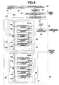
- Fig. 4 shows the third embodiment of the present invention.
- components identical to those in Figs. 1 and 3 are assigned the same reference numerals. The description of the components will be omitted.
- the embodiment shown in Fig. 4 enables compression or stretch in both the horizontal and vertical directions of a screen, and differs from the embodiments shown in Figs. 1 and 3 in a point that a clock oscillatory circuit 65 is adopted instead of the clock oscillatory circuit 15 or 45.
- the clock oscillatory circuit 65 comprises a VCO 18, clock generator 16, H clock circuit 19, and V clock circuit 47.
- a switch 32 in the H clock circuit 19 outputs a clock e11 whose clock frequency varies within one horizontal scanning period.
- a switch 52 in the V clock circuit 47 outputs a clock f2 whose clock frequency varies within one vertical scanning period.
- a liquid-crystal panel 25 has an aspect ratio of 16:9 and an input video signal (for example an NTSC broadcast signal) indicates an aspect ratio of 4:3, if the horizontal or vertical reference clock alone is used, as shown in Fig. 6, a picture stretching sideways or contracting lengthwise as shown in Fig. 6 ensues.
- the selection by the switches 32 and 52 enables suppression of the sideways stretch (lengthwise contraction) phenomenon.
- part of a picture to be displayed on a liquid-crystal panel 25 appearing in the center of a screen is compressed in the horizontal direction and stretched in the vertical direction.
- Parts of the picture appearing at the right-hand and left-hand edges of the screen are stretched in the horizontal direction, and parts thereof appearing at the upper and lower edges thereof are compressed in the vertical direction. Consequently, the roundness in the center of a screen improves, and a picture not give a sense of incompatibility ensues.
- compression and stretch can be performed arbitrarily in the horizontal and vertical directions according to an input video signal.
- a picture not giving a sense of incompatibility can be displayed.
- a general liquid-crystal display has been described.
- the present invention can apply to a projection type liquid-crystal display.
Landscapes
- Engineering & Computer Science (AREA)
- Multimedia (AREA)
- Signal Processing (AREA)
- Physics & Mathematics (AREA)
- Computer Hardware Design (AREA)
- General Physics & Mathematics (AREA)
- Theoretical Computer Science (AREA)
- Computer Graphics (AREA)
- Liquid Crystal Display Device Control (AREA)
- Transforming Electric Information Into Light Information (AREA)
- Investigating Or Analyzing Materials By The Use Of Ultrasonic Waves (AREA)
- Liquid Crystal (AREA)
Applications Claiming Priority (3)
| Application Number | Priority Date | Filing Date | Title |
|---|---|---|---|
| JP244915/95 | 1995-09-22 | ||
| JP24491595 | 1995-09-22 | ||
| JP7244915A JPH0993517A (ja) | 1995-09-22 | 1995-09-22 | 液晶表示装置 |
Publications (3)
| Publication Number | Publication Date |
|---|---|
| EP0765078A2 true EP0765078A2 (de) | 1997-03-26 |
| EP0765078A3 EP0765078A3 (de) | 1997-06-18 |
| EP0765078B1 EP0765078B1 (de) | 2001-08-01 |
Family
ID=17125872
Family Applications (1)
| Application Number | Title | Priority Date | Filing Date |
|---|---|---|---|
| EP96306687A Expired - Lifetime EP0765078B1 (de) | 1995-09-22 | 1996-09-16 | Flüssigkristallanzeigevorrichtung |
Country Status (7)
| Country | Link |
|---|---|
| US (1) | US5940061A (de) |
| EP (1) | EP0765078B1 (de) |
| JP (1) | JPH0993517A (de) |
| KR (1) | KR100223118B1 (de) |
| CN (1) | CN1104653C (de) |
| DE (2) | DE69614210T2 (de) |
| TW (1) | TW324790B (de) |
Cited By (6)
| Publication number | Priority date | Publication date | Assignee | Title |
|---|---|---|---|---|
| EP0984422A2 (de) | 1998-08-31 | 2000-03-08 | Semiconductor Energy Laboratory Co., Ltd. | Anzeigevorrichtung und Steuerverfahren dafür |
| WO2002032148A1 (en) * | 2000-10-11 | 2002-04-18 | Sony Electronics Inc. | Adaptive clocking mechanism for digital video decoder |
| EP1161108A4 (de) * | 2000-01-12 | 2003-01-02 | Mitsubishi Electric Corp | Mobiles kommunikationsendgerät |
| EP1056285A3 (de) * | 1999-05-28 | 2003-09-17 | Alps Electric Co., Ltd. | Videoanzeigegerät zum Anzeigen von Videosignalen nach mehreren Arten mit verschiedenen Spezifikationen |
| EP0797183B1 (de) * | 1996-03-22 | 2006-08-23 | Sharp Kabushiki Kaisha | Matrixanzeigevorrichtung und Verfahren zu ihrer Ansteuerung |
| US8659628B2 (en) | 2010-10-27 | 2014-02-25 | Au Optronics Corp. | Method for controlling gate signals and device thereof |
Families Citing this family (22)
| Publication number | Priority date | Publication date | Assignee | Title |
|---|---|---|---|---|
| US5796392A (en) | 1997-02-24 | 1998-08-18 | Paradise Electronics, Inc. | Method and apparatus for clock recovery in a digital display unit |
| JP3472679B2 (ja) * | 1997-03-19 | 2003-12-02 | 株式会社日立製作所 | 液晶駆動回路及び液晶表示装置 |
| US6791518B2 (en) * | 1997-04-18 | 2004-09-14 | Fujitsu Display Technologies Corporation | Controller and control method for liquid-crystal display panel, and liquid-crystal display device |
| JP2000020015A (ja) * | 1998-07-03 | 2000-01-21 | Toshiba Corp | 画像表示装置及びその方法 |
| JP3432747B2 (ja) * | 1998-07-14 | 2003-08-04 | シャープ株式会社 | 液晶表示装置の駆動装置および駆動方法 |
| KR100532389B1 (ko) * | 1998-08-10 | 2006-01-27 | 삼성전자주식회사 | 액정 판넬 구동용 전압 발생장치 및 방법 |
| US6157376A (en) * | 1998-09-30 | 2000-12-05 | Genesis Microchip, Corp. | Method and apparatus for generating a target clock signal having a frequency of X/Y times the frequency of a reference clock signal |
| JP3644672B2 (ja) | 1999-07-09 | 2005-05-11 | シャープ株式会社 | 表示装置およびその駆動方法 |
| KR100563826B1 (ko) * | 1999-08-21 | 2006-04-17 | 엘지.필립스 엘시디 주식회사 | 액정표시장치의 데이타구동회로 |
| JP4547737B2 (ja) * | 1999-08-31 | 2010-09-22 | ソニー株式会社 | 投射型表示装置 |
| JP2001109437A (ja) * | 1999-10-12 | 2001-04-20 | Fujitsu Ltd | 液晶パネルの駆動回路及び液晶制御信号発生回路とそれらを備えた液晶表示装置及び液晶表示装置の制御方法 |
| KR100330037B1 (ko) * | 2000-07-06 | 2002-03-27 | 구본준, 론 위라하디락사 | 액정표시장치 및 그 구동방법 |
| KR100759971B1 (ko) * | 2001-01-26 | 2007-09-18 | 삼성전자주식회사 | 입력 영상의 어스펙트 모드에 적응하는 액정 표시 장치 |
| JP2003098992A (ja) * | 2001-09-19 | 2003-04-04 | Nec Corp | ディスプレイの駆動方法、その回路及び携帯用電子機器 |
| JP4094479B2 (ja) * | 2003-05-06 | 2008-06-04 | 株式会社ナナオ | 焼き付き軽減装置及びこれを備えた画像表示装置 |
| KR100580176B1 (ko) * | 2003-09-17 | 2006-05-15 | 삼성전자주식회사 | 디지털 방송 수신 시스템에서 디스플레이 동기 신호 생성장치 |
| JP2005316298A (ja) * | 2004-04-30 | 2005-11-10 | Nec Lcd Technologies Ltd | 液晶表示装置、該液晶表示装置に用いられる光源駆動回路及び光源駆動方法 |
| KR101803987B1 (ko) | 2010-01-20 | 2017-12-01 | 가부시키가이샤 한도오따이 에네루기 켄큐쇼 | 표시 장치 |
| JP7075752B2 (ja) * | 2016-12-23 | 2022-05-26 | 株式会社半導体エネルギー研究所 | データ変換回路、および表示装置 |
| US10553167B2 (en) | 2017-06-29 | 2020-02-04 | Japan Display Inc. | Display device |
| JP2019109353A (ja) | 2017-12-18 | 2019-07-04 | シャープ株式会社 | 表示制御装置および該表示制御装置を備えた液晶表示装置 |
| CN110910828B (zh) * | 2018-09-14 | 2022-01-11 | 华为技术有限公司 | 一种屏幕模组及电子设备 |
Family Cites Families (7)
| Publication number | Priority date | Publication date | Assignee | Title |
|---|---|---|---|---|
| JP2673386B2 (ja) * | 1990-09-29 | 1997-11-05 | シャープ株式会社 | 映像表示装置 |
| JPH04324420A (ja) * | 1991-04-24 | 1992-11-13 | Asahi Glass Co Ltd | 液晶表示装置 |
| JPH0514844A (ja) * | 1991-07-05 | 1993-01-22 | Matsushita Electric Ind Co Ltd | 液晶パネル駆動制御回路 |
| JP2759727B2 (ja) * | 1992-04-22 | 1998-05-28 | 日本ビクター株式会社 | ディスプレイ装置 |
| JPH0659643A (ja) * | 1992-08-04 | 1994-03-04 | Fujitsu General Ltd | 液晶表示装置の歪補正方法 |
| JPH06189231A (ja) * | 1992-12-16 | 1994-07-08 | Toshiba Corp | 液晶表示装置 |
| JP2531426B2 (ja) * | 1993-02-01 | 1996-09-04 | 日本電気株式会社 | マルチスキャン型液晶ディスプレイ装置 |
-
1995
- 1995-09-22 JP JP7244915A patent/JPH0993517A/ja active Pending
-
1996
- 1996-08-06 TW TW085109512A patent/TW324790B/zh active
- 1996-09-16 DE DE69614210T patent/DE69614210T2/de not_active Expired - Fee Related
- 1996-09-16 EP EP96306687A patent/EP0765078B1/de not_active Expired - Lifetime
- 1996-09-16 DE DE0765078T patent/DE765078T1/de active Pending
- 1996-09-19 KR KR1019960040784A patent/KR100223118B1/ko not_active Expired - Fee Related
- 1996-09-20 US US08/717,019 patent/US5940061A/en not_active Expired - Fee Related
- 1996-09-20 CN CN96112835A patent/CN1104653C/zh not_active Expired - Fee Related
Cited By (8)
| Publication number | Priority date | Publication date | Assignee | Title |
|---|---|---|---|---|
| EP0797183B1 (de) * | 1996-03-22 | 2006-08-23 | Sharp Kabushiki Kaisha | Matrixanzeigevorrichtung und Verfahren zu ihrer Ansteuerung |
| EP0984422A2 (de) | 1998-08-31 | 2000-03-08 | Semiconductor Energy Laboratory Co., Ltd. | Anzeigevorrichtung und Steuerverfahren dafür |
| US7782315B2 (en) | 1998-08-31 | 2010-08-24 | Semiconductor Energy Laboratory Co., Ltd | Display device and method of driving the same |
| EP1056285A3 (de) * | 1999-05-28 | 2003-09-17 | Alps Electric Co., Ltd. | Videoanzeigegerät zum Anzeigen von Videosignalen nach mehreren Arten mit verschiedenen Spezifikationen |
| EP1161108A4 (de) * | 2000-01-12 | 2003-01-02 | Mitsubishi Electric Corp | Mobiles kommunikationsendgerät |
| US7039436B1 (en) | 2000-01-12 | 2006-05-02 | Mitsubishi Denki Kabushiki Kaisha | Mobile communication terminal |
| WO2002032148A1 (en) * | 2000-10-11 | 2002-04-18 | Sony Electronics Inc. | Adaptive clocking mechanism for digital video decoder |
| US8659628B2 (en) | 2010-10-27 | 2014-02-25 | Au Optronics Corp. | Method for controlling gate signals and device thereof |
Also Published As
| Publication number | Publication date |
|---|---|
| CN1104653C (zh) | 2003-04-02 |
| EP0765078A3 (de) | 1997-06-18 |
| DE69614210D1 (de) | 2001-09-06 |
| DE69614210T2 (de) | 2002-05-08 |
| KR100223118B1 (ko) | 1999-10-15 |
| DE765078T1 (de) | 1997-10-09 |
| US5940061A (en) | 1999-08-17 |
| TW324790B (en) | 1998-01-11 |
| KR970019540A (ko) | 1997-04-30 |
| JPH0993517A (ja) | 1997-04-04 |
| EP0765078B1 (de) | 2001-08-01 |
| CN1165970A (zh) | 1997-11-26 |
Similar Documents
| Publication | Publication Date | Title |
|---|---|---|
| US5940061A (en) | Liquid-crystal display | |
| JPS59105776A (ja) | 電子ビユ−フアインダ装置 | |
| EP1056285A2 (de) | Videoanzeigegerät zum Anzeigen von Videosignalen nach mehreren Arten mit verschiedenen Spezifikationen | |
| KR19980081010A (ko) | 평면표시장치 및 표시방법 | |
| JP2000184317A (ja) | 投射型マルチ画面ディスプレイ装置 | |
| EP0797183A1 (de) | Matrixanzeigevorrichtung und Verfahren zu ihrer Ansteuerung | |
| JPS6253989B2 (de) | ||
| JP3623304B2 (ja) | 液晶表示装置 | |
| JPH08331486A (ja) | 画像表示装置 | |
| KR0147597B1 (ko) | 와이드 텔레비젼 수상기용 액정패널 구동장치 | |
| KR100405275B1 (ko) | 문자표시장치 | |
| JPH07325551A (ja) | 画素配列表示装置 | |
| JPH07168542A (ja) | 液晶表示装置 | |
| JPH07319420A (ja) | 画素同期装置 | |
| JP3421987B2 (ja) | クロック調整回路及びそれを用いた画像表示装置 | |
| JP3804893B2 (ja) | 映像信号処理回路 | |
| JPH0662339A (ja) | 2画面表示テレビ受信機 | |
| JPH05341739A (ja) | 画面分割装置 | |
| JP2001343951A (ja) | 液晶駆動装置およびその駆動方法 | |
| JPH0683419B2 (ja) | テレビジョン信号受信装置 | |
| JPH0435284A (ja) | 液晶表示装置 | |
| JPH0497670A (ja) | 液晶表示装置 | |
| JPH09307786A (ja) | 画像表示装置 | |
| KR100490933B1 (ko) | 디스플레이시스템및영상신호를디스플레이시스템에공급하는방법 | |
| JPH09270976A (ja) | 液晶表示装置 |
Legal Events
| Date | Code | Title | Description |
|---|---|---|---|
| PUAI | Public reference made under article 153(3) epc to a published international application that has entered the european phase |
Free format text: ORIGINAL CODE: 0009012 |
|
| 17P | Request for examination filed |
Effective date: 19961004 |
|
| AK | Designated contracting states |
Kind code of ref document: A2 Designated state(s): DE FR GB |
|
| PUAL | Search report despatched |
Free format text: ORIGINAL CODE: 0009013 |
|
| EL | Fr: translation of claims filed | ||
| AK | Designated contracting states |
Kind code of ref document: A3 Designated state(s): DE FR GB |
|
| DET | De: translation of patent claims | ||
| 17Q | First examination report despatched |
Effective date: 19991012 |
|
| GRAG | Despatch of communication of intention to grant |
Free format text: ORIGINAL CODE: EPIDOS AGRA |
|
| GRAG | Despatch of communication of intention to grant |
Free format text: ORIGINAL CODE: EPIDOS AGRA |
|
| GRAH | Despatch of communication of intention to grant a patent |
Free format text: ORIGINAL CODE: EPIDOS IGRA |
|
| GRAH | Despatch of communication of intention to grant a patent |
Free format text: ORIGINAL CODE: EPIDOS IGRA |
|
| GRAA | (expected) grant |
Free format text: ORIGINAL CODE: 0009210 |
|
| AK | Designated contracting states |
Kind code of ref document: B1 Designated state(s): DE FR GB |
|
| REF | Corresponds to: |
Ref document number: 69614210 Country of ref document: DE Date of ref document: 20010906 |
|
| ET | Fr: translation filed | ||
| REG | Reference to a national code |
Ref country code: GB Ref legal event code: IF02 |
|
| PLBE | No opposition filed within time limit |
Free format text: ORIGINAL CODE: 0009261 |
|
| STAA | Information on the status of an ep patent application or granted ep patent |
Free format text: STATUS: NO OPPOSITION FILED WITHIN TIME LIMIT |
|
| 26N | No opposition filed | ||
| PGFP | Annual fee paid to national office [announced via postgrant information from national office to epo] |
Ref country code: DE Payment date: 20040909 Year of fee payment: 9 |
|
| PGFP | Annual fee paid to national office [announced via postgrant information from national office to epo] |
Ref country code: GB Payment date: 20040915 Year of fee payment: 9 |
|
| PGFP | Annual fee paid to national office [announced via postgrant information from national office to epo] |
Ref country code: FR Payment date: 20050823 Year of fee payment: 10 |
|
| PG25 | Lapsed in a contracting state [announced via postgrant information from national office to epo] |
Ref country code: GB Free format text: LAPSE BECAUSE OF NON-PAYMENT OF DUE FEES Effective date: 20050916 |
|
| PG25 | Lapsed in a contracting state [announced via postgrant information from national office to epo] |
Ref country code: DE Free format text: LAPSE BECAUSE OF NON-PAYMENT OF DUE FEES Effective date: 20060401 |
|
| GBPC | Gb: european patent ceased through non-payment of renewal fee |
Effective date: 20050916 |
|
| REG | Reference to a national code |
Ref country code: FR Ref legal event code: ST Effective date: 20070531 |
|
| PG25 | Lapsed in a contracting state [announced via postgrant information from national office to epo] |
Ref country code: FR Free format text: LAPSE BECAUSE OF NON-PAYMENT OF DUE FEES Effective date: 20061002 |