EP0766258A2 - DRAM-Signalspielraumprüfverfahren - Google Patents
DRAM-Signalspielraumprüfverfahren Download PDFInfo
- Publication number
- EP0766258A2 EP0766258A2 EP96305900A EP96305900A EP0766258A2 EP 0766258 A2 EP0766258 A2 EP 0766258A2 EP 96305900 A EP96305900 A EP 96305900A EP 96305900 A EP96305900 A EP 96305900A EP 0766258 A2 EP0766258 A2 EP 0766258A2
- Authority
- EP
- European Patent Office
- Prior art keywords
- sense amp
- bit line
- signal
- sense
- data
- Prior art date
- Legal status (The legal status is an assumption and is not a legal conclusion. Google has not performed a legal analysis and makes no representation as to the accuracy of the status listed.)
- Granted
Links
Images




Classifications
-
- G—PHYSICS
- G11—INFORMATION STORAGE
- G11C—STATIC STORES
- G11C11/00—Digital stores characterised by the use of particular electric or magnetic storage elements; Storage elements therefor
- G11C11/21—Digital stores characterised by the use of particular electric or magnetic storage elements; Storage elements therefor using electric elements
- G11C11/34—Digital stores characterised by the use of particular electric or magnetic storage elements; Storage elements therefor using electric elements using semiconductor devices
- G11C11/40—Digital stores characterised by the use of particular electric or magnetic storage elements; Storage elements therefor using electric elements using semiconductor devices using transistors
- G11C11/401—Digital stores characterised by the use of particular electric or magnetic storage elements; Storage elements therefor using electric elements using semiconductor devices using transistors forming cells needing refreshing or charge regeneration, i.e. dynamic cells
- G11C11/4063—Auxiliary circuits, e.g. for addressing, decoding, driving, writing, sensing or timing
- G11C11/407—Auxiliary circuits, e.g. for addressing, decoding, driving, writing, sensing or timing for memory cells of the field-effect type
- G11C11/409—Read-write [R-W] circuits
- G11C11/4091—Sense or sense/refresh amplifiers, or associated sense circuitry, e.g. for coupled bit-line precharging, equalising or isolating
-
- G—PHYSICS
- G11—INFORMATION STORAGE
- G11C—STATIC STORES
- G11C29/00—Checking stores for correct operation ; Subsequent repair; Testing stores during standby or offline operation
- G11C29/04—Detection or location of defective memory elements, e.g. cell constructio details, timing of test signals
- G11C29/50—Marginal testing, e.g. race, voltage or current testing
-
- G—PHYSICS
- G06—COMPUTING OR CALCULATING; COUNTING
- G06F—ELECTRIC DIGITAL DATA PROCESSING
- G06F2201/00—Indexing scheme relating to error detection, to error correction, and to monitoring
- G06F2201/81—Threshold
-
- G—PHYSICS
- G11—INFORMATION STORAGE
- G11C—STATIC STORES
- G11C11/00—Digital stores characterised by the use of particular electric or magnetic storage elements; Storage elements therefor
- G11C11/21—Digital stores characterised by the use of particular electric or magnetic storage elements; Storage elements therefor using electric elements
- G11C11/34—Digital stores characterised by the use of particular electric or magnetic storage elements; Storage elements therefor using electric elements using semiconductor devices
- G11C11/40—Digital stores characterised by the use of particular electric or magnetic storage elements; Storage elements therefor using electric elements using semiconductor devices using transistors
- G11C11/401—Digital stores characterised by the use of particular electric or magnetic storage elements; Storage elements therefor using electric elements using semiconductor devices using transistors forming cells needing refreshing or charge regeneration, i.e. dynamic cells
Definitions
- the present invention relates generally to semiconductor memories and more particularly to methods of testing semiconductor memories.
- Memory cell defects and memory array defects have many sources and, as a result, many signatures. While single, isolated cell failures may be scattered throughout the array, very often, multiple cells in the same vicinity fail. When multi-cell failures occur, these failures may be characterised as a word line failure, (i.e. failing cells with the same word line address), a bit (or column) line failure (i.e. failing cells with the same bit address), or both. The sources of these multi-cell failures vary. Consequently, memory arrays are tested extensively to identify defective cells.
- FIG. 1 is a schematic representation of a prior art wide Input/Output (I/O) 16Mb DRAM chip.
- the chip 100 is organised with two Redundant Bit Lines (RBL) 102 and 104 providing two spare columns in each subarray 106.
- Each subarray 106 includes 2 n Bit Line (BL) pairs 108 (where n is typically between 5 and 8) and one or more redundant bit line pairs (2 in this example).
- BL Bit Line
- Each of the subarrays 106 is part of a subarray block 110. All of the subarray blocks 110, collectively, form the entire RAM array. So, for example, a 16Mb RAM has 16 blocks 110 of 1Mb each. Block size, subarray size and the number of subarrays 106 per block 110 are interdependent and, selected based on performance and design objectives.
- Multiple bits of a subarray block 110 are accessed (read from or written to) when one word line 112 is selected and driven high. Data from accessed cells are provided simultaneously to the bit lines 108 and redundant bit lines 102 and 104. After a predetermined minimum delay, a delay sufficient to allow the redundancy decoder to determine whether a spare column is addressed, a single bit line 108 or a redundant bit line 102, 104 is selected in each subarray 106. In each subarray, the selected bit line 108 or redundant bit line 102, 104 is coupled to a Local Data Line (LDL) 114. LDLs 114 are coupled to Master Data Lines (MDLs) 116. The MDLs 116 couple corresponding subarrays 106 in each subarray block 110. Data is transferred between the subarrays 106 and the chip I/O's on the MDLs 116.
- LDL Local Data Line
- MDLs Master Data Lines
- FIG. 2 is a transistor level cross-sectional schematic of a bit line 108 in a subarray 106.
- Cells 120, 122 connected to adjacent word lines 112, 118 also are connected to opposite lines 124, 126 of each bit line pair.
- half of the word lines 112 e.g., word lines with even addresses
- the remaining half of the word lines 118, (odd addressed word lines) select the cells 122 on the other lines 126 of the bit line pair.
- Each cell's storage capacitor (C S ) 128 is, typically, a trench capacitor or a stacked structure for array density.
- Each bit line 124, 126 has essentially the same capacitance (C BL ).
- the magnitude of the bit line signal is C S *V S /(C S +C BL ) .
- V SIG bit line signal
- This boosted level, called V pp is normally generated on-chip.
- V PP V dd +V T
- V SIG ⁇ C S (V dd /2)/(C S +C BL ) .
- the circuit of FIG. 2A operates according to the timing diagram of FIG. 2B.
- a "one" is stored in any cell 120, 122 by charging the cell's storage capacitor 128, 138.
- the array Prior to selecting a cell 120 or 122, the array is at its steady-state standby or pre-charge condition.
- the voltage on the bit line pair 124, 126 is pulled to V dd /2 and equalised by equalisation transistor 134 because equalisation signal EQ on its gate 132 is high.
- the Word Lines (WL) 112, 118 and Column SeLect (CSL) lines 136 are held low during standby. In prior art RAMs, each word line was clamped low (unless driven high) by a simple resetable latch (not shown).
- bit line capacitance is at least one order of magnitude larger than the storage capacitor 128. So, V SIG is normally at least an order of magnitude smaller than V dd .
- V SIG is normally at least an order of magnitude smaller than V dd .
- the sense amp 140 After a delay sufficient to develop V SIG , i.e. to transfer V S to the bit line, the sense amp 140 is set by driving the Sense Amp Enable (SAE) line 142 high and, subsequently, by pulling its inverse ( SAE ⁇ ) 144 low.
- SAE Sense Amp Enable
- V SIG is amplified and re-driven on the bit line pair 124, 126 by the sense amp, which forces 124, 126 High/Low or Low/High depending on data stored in the cell 120. Simultaneously with re-driving the bit line pair, the sense amp writes the sensed data back into the selected cell 120.
- CSL Column SeLect signal
- One source of cell failures stems from inadequate (cell) signal margin.
- all of the cells may appear good.
- C S may not be fully discharged (known as a weak "0").
- these cells may not consistently reflect the data written into them.
- Such a failing cell may appear acceptable under test conditions, but when used in system memory, the cell may fail, intermittently. So, it is important to identify such cells (with marginal stored data levels) during test.
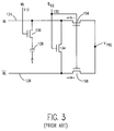
- FIG. 3 represents a bit line pair 124, 126 upon which cell signal margin may be tested by a prior art approach.
- the bit line pre-charge voltage V PRE is varied. Normally, as described for FIG. 2A, ⁇ EQ 132 is high during restore and low during sense.
- Pre-charge FETs 156, 158 are connected between V PRE and bit lines 126, 124 respectively.
- V PRE is set to V dd /2.
- V PRE voltage-to-V TN
- V SIG is dependant upon V PRE
- varying V PRE significantly from V dd /2 alters the time it takes for V SIG to develop. Altering this time makes it difficult to determine whether testing failures are due to poor signal margin and, therefore, real or, instead, the result of not allowing adequate time for signal development and, therefore, false errors.
- DRAM Dynamic Random Access Memory
- the step of writing the reduced signal comprises the steps of: i) driving a plurality of word lines high; ii) forcing a sense amp enable and a plurality of bit lines to a test voltage level; and iii) driving the word lines low.
- the step of reading data from each cell comprises the steps of: i) driving a selected word line high; ii) enabling sense amps after a signal develops on the bit lines in response to the selected word line, the sense amp setting in response to the signal; iii) selectively coupling the set sense amp to a Local Data Line (LDL), whereby the data is driven onto the LDL; and, the iv) latching the data into the sense amp.
- LDL Local Data Line
- a control circuit uses the equalisation voltage to disable the sense amp.
- cell signal margin may be tested in a new way.
- cell signal margin is tested by varying the cell signal V S .
- V S may be selected, to determine both a high and a low signal margin.
- a bit line pair is coupled through a pair of high-resistance pass gates to a sense amp. During sense, the high-resistance pass gates act in conjunction with the charge stored on the bit line pair as, effectively, a high-resistance passive load for the sense amp.
- a control circuit selectively switches on and off bit line equalisation coincident with selectively passing either the equalisation voltage or set voltages to the sense amp and an active sense amp load. Further, after it is set, the sense amp is selectively connected to LDLs through low-resistance column select pass gates. Therefore, the sense amp quickly discharges one of the connected LDL pair while the bit line voltage remains essentially unchanged. Thus, data is passed from the sense amp to a second sense amplifier and off chip. After data is passed to the LDLs, the control circuit enables the active sense amp load to pull the sense amp high side to a full up level.
- a method embodying the present invention has the advantage that it reduces semiconductor memory test time and simplifies semiconductor memory test. The time required to identify defective semiconductor memory chips is reduced and initial semiconductor memory chip test screening is simplified.
- a method embodying the present invention has the advantage that it increases RAM signal test accuracy, reduces RAM chip area dedicated for signal test and reduces test induced noise during RAM cell signal margin tests.
- a bit line pair is coupled through a pair of high-resistance pass gates to a sense amp.
- the high-resistance pass gates act in conjunction with the charge stored on the bit line pair as, effectively, a high-resistance passive load for the sense amp.
- a control circuit selectively switches on and off bit line equalisation coincident with selectively passing either the equalisation voltage or set voltages to enable the sense amp. Further, after it is set, the sense amp is selectively connected to LDLs, which are pre-charged to V dd , through low-resistance column select pass gates.
- the column select pass gates which are NFETs, allow passing data to the LDLs prior to setting the active sense amp load even though the LDLs are pre-charged to V dd .
- the NFET threshold prevents the V dd pre-charge from destroying the sensed data. Therefore, the sense amp quickly discharges one of the connected LDL pair while the bit line voltage remains essentially unchanged.
- data is passed from the sense amp to a second sense amplifier and off chip.
- the control circuit enables the active sense amp load to pull the sense amp high side to a full up level.
- the gate voltage on the high resistance pass gates is boosted to reduce their select resistance in order to quickly write the sensed data back into the array.
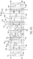
- FIG. 4A schematically represents an array cross section with a sense amp shared by two bit line pairs and FIG. 4B is a schematic of control logic therefor according to the present invention. It is intended that each sense amp may be connected to a single bit line pair, or to two or more bit line pairs without departing from the spirit of the present invention.
- FIG. 4C is a block diagram of the sense amp, column switch and mux of FIG. 4A.
- FIG. 4A shows the sense amp 166 shared by two bit line pairs, a right pair and a left pair. For convenience these pairs, and elements in each pair, are labelled L and R. Thus, the cell in the left pair is designated 160L and the cell in the right pair is designated 160R.
- Each bit line pair includes an equalisation circuit 162L, 162R, gated by a restore line 163L, 163R, which operates substantially as described above. Additionally, in this shared sense amp configuration, each bit line pair is coupled to the sense amp by a pair high-resistance pass gates 164L or 164R, which are half of a multiplexor (mux). Each pair is referred to herein as a mux half 164L, 164R.
- the mux 164 (164L combined with 164R) is controlled by select lines 165L, 165R, respectively, to selectively couple the selected bit line pair to the sense amp 166.
- the sense amp 166 is a pair of cross coupled NFETs 168, 170 and is enabled by ⁇ N from the control circuit 185 in Fig. 4B. ⁇ N is connected to the sources of NFETs 168, 170.
- the sense amp 166 output is connected to the mux 164 at sense amp output pair BL, BL ⁇ .
- the sense amp is designed to minimise the capacitance on BL, BL ⁇ so that during a READ, the bit line pair sees a low RC in the mux direction, as indicated by the arrow labelled I SIG in FIG. 4C.
- the sense amp 166 sees a high RC in the mux direction, as indicated by the arrow labelled I SA in FIG. 4C. Therefore, when the sense amp is coupled to a bit line pair through a mux half 164L, 164R, the signal on the bit line pair is passed to the sense amp, substantially unaffected.
- the mux pass gates act as load resistors for the sense amp and the voltages on the bit line pair remain essentially unaffected.
- column switch 176 which is a pair of low resistance NFET pass gates 178, 180.
- Column switch 176 connects the sense amp 166 output at BL, BL ⁇ to Local Data Lines (LDLs) 182, 184, when CSL i 186 is high.
- LDLs Local Data Lines
- These column switch pass gates 178, 180 have a substantially lower on resistance than the mux half 164L, 164R pass gates. Therefore, when the set sense amp 166 is connected to the LDLs through the column switch 176, the primary current through the sense amp 166 is I LDL from the LDLs, even though a mux half 164L, 164R remains selected and current continues to flow through the selected mux half.
- the column switch 176 is a pair of NFETs, the potential disturb from coupling the charged (to V dd ) LDL capacitances to the sense amp is essentially eliminated.
- the NFET pass gates because of the NFET threshold voltage, effectively attenuate the noise that is normally introduced in such coupling. Thus, the disturb is eliminated.
- LDLs 182, 184 are connected through the MDLs to a traditional sense amp (not shown). This second sense amp exploits the advantages provided by the present invention to improve performance by amplifying the sense amp 166 output as soon as the sense amp 166 places sufficient signal on the LDLs 182, 184.
- an active sense amp load a pair of cross coupled PFETs 172, 174, connected to the sense amp 166 output pair BL, BL ⁇ , latches the data sensed thereby and provides a full V dd up level and reinforces and during a normal write.
- ⁇ P the active sense amp load enable from control circuit 185, is connected to the sources of cross coupled PFETs 172, 174.
- U.S.-A- 5,267,214 teaches a RAM wherein the bit lines are connected to the sense amp by low resistance pass gates.
- the low resistance of the pass gates of U.S.-A- 5,267,214 is further reduced when, after enabling and setting the NFET half of the sense amp, the drive to the bit line pass gates is boosted above V dd coincident with enabling the PFET portion of the sense amp.
- the sense amp drives full voltage levels back into the bit line pair. Only after setting this PFET half of the sense amp of U.S.-A- 5,267,214 are the column select pass gates opened, thus delaying data from being driven off chip.
- the mux select line is boosted above V dd to gate full levels to the bit line pair from the sense amp 166 and the active sense amp load.
- V dd the mux select line is boosted above V dd to gate full levels to the bit line pair from the sense amp 166 and the active sense amp load.
- the special control circuit 185 of FIG. 4B provides both normal control and test-specific control for the array, the sense amp and the active sense amp load.
- Control circuit 185 input, Test control SIGnal T SIG remains high and is driven low during test only.
- T SIG is NANDed with ⁇ SA in NAND gate 190 to generate Sense Amp Enable SAE ⁇ .
- SAE ⁇ is connected directly to the gates of NFETs 192, 194, which are connected between V PRE and ⁇ P or ⁇ N , respectively. So, the state of SAE ⁇ selects the level of both sense amp enable/disable phase ⁇ N and active sense amp load enable/disable phase ⁇ P .
- SAE ⁇ is the input to inverter 196.
- inverter 196 SAE
- SAE is connected to the gate of NFET 198 which is connected between ⁇ N and ground.
- SA E ⁇ is the input of delay 200, the output of which is connected to the gate of PFET 202.
- PFET 202 is connected between V dd and ⁇ P to provide a corresponding path to V dd for cross coupled PFETs 172, 174.
- T SIG is also NANDed in one or more NAND gates, represented by single NAND gate 204, with ⁇ EQ to generate ⁇ PREL and ⁇ PRER ( ⁇ PREL,R ).
- ⁇ EQ is two independent signals ⁇ EQL and ⁇ EQR , which are each NANDed with T SIG .
- an additional L/R select signal may be NANDed with ⁇ EQ and T SIG to generate ⁇ PREL,R .
- ⁇ PREL and ⁇ PRER may be, simply, identical signals generated from NANDing ⁇ EQ and T SIG .
- NFET 198 selectively provides a path to ground for the sense amplifier 160, when it is turned on and PFET 202 selectively provides a path to V dd for the sense amplifier active load, when it is turned on.
- delay 200 is delayed by delay 200 until after the sense amp is set and passed through the column switch 176 to LDLs 182, 184.
- delay 200 is a simple polysilicon RC delay with inverters for re-forming the signal therefrom.
- delay 200 is an even number of series connected inverters and, more particularly, between 6 and 8 inverters.
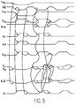
- FIG. 5 is a timing diagram for performing a signal margin test on the array of FIG. 4A using the logic of FIG. 4B according to the preferred embodiment of the present invention.
- FIG. 6 is a flow diagram for testing a DRAM according to the preferred embodiment of the present invention.
- T SIG is tied high.
- RAS ⁇ which provides a typical DRAM select function, drives a typical timing chain that selects and drives the word line WL, bit line equalisation signal ⁇ EQ and sense amp enable signal ⁇ SA .
- V PRE is held at V dd /2 and is varied therefrom only during test.
- V PRE is from a controllable, variable voltage power supply that provides a tester controlled supply voltage. All other voltages are within their normal operating limits or slightly beyond during test.
- NFETs 192, 194 couple V PRE to ⁇ N and ⁇ P , normally, during standby, when RAS ⁇ is high, but also during test, when both T SIG and RAS ⁇ are low.
- ⁇ PREL , ⁇ PRER are low only when equalisation signal ⁇ EQ and Test control SIGnal T SIG are both high. So, the pair of lines in each bit line pair are tied together and to V PRE when RAS ⁇ is high, but also during test, when both T SIG and RAS ⁇ are low.
- V PRE is uncoupled from the bit lines and sense amp during sense.
- ⁇ P , ⁇ N , and ⁇ PREL,R are common lines provided to multiple bit lines.
- the control of ⁇ P , ⁇ N , and ⁇ PREL,R may be generated individually for each bit line pair.
- measuring cell signal margin is, basically, a two step test.
- a reduced signal is written to all of the cells 160L, 160R.
- the bit line voltage level is forced to a test voltage level, V TEST .
- V TEST is a level offset from V dd or ground by some fraction of V dd .
- Loading the test voltage effectively writes a weak "1" or "0" into the array.
- the second basic step 242 the array is read, normally, to determine if the reduced signal can be sensed (read) correctly.
- a DRAMs signal margin may be determined.
- the Block Write step 240 begins when RAS ⁇ and T SIG are driven low 244.
- V PRE is ramped up or down (down in this example) to V TEST 246.
- T SIG is low, all of the word lines WLL and WLR are driven high simultaneously to write the weak signal (V PRE ) into the entire array.
- V PRE weak signal
- only a portion of the array may be tested by selecting and driving an individual word line or a subset of word lines.
- Timing Equalisation control phase ⁇ EQ is driven high with the word lines WLL and WLR as during a normal access cycle. However, because T SIG is low, ⁇ EQ is blocked so that ⁇ PREL,R remains high.
- timing Sense Amp control phase ⁇ SA also rises but, is also blocked, because T SIG is low. So, ⁇ P and ⁇ N remain at V PRE and the sense amp 166 remains disabled.
- V PRE test voltage level
- RAS ⁇ rises ending the write operation, placing the RAM in standby (pre-charge).
- the sense amp remains disabled and the bit lines remain clamped at V PRE because ⁇ N and ⁇ P are clamped at V PRE and pre-charge (equalisation) signals ⁇ PREL,R remain high.
- step 252 V PRE is ramped back to V dd /2, pulling all of the bit line pairs and both ⁇ N and ⁇ P back to V dd /2. T SIG is held low until V PRE is returned to V dd /2. Once T SIG rises 252, the Block Write step 240 is complete and the RAM is in its normal operating condition.
- the RAM array is READ 254, 256 to determine whether any cell's signal limit has been exceeded 258.
- a correct result during the READ indicates that the signal limit has not been exceeded 260 and that some signal margin remains. Therefore, if, in spite of the reduced signal level V S , every cell reads correctly 258 (as a low in this example) then, the entire test is repeated with slightly less signal 262 (a slightly higher V PRE level in this example). This test may be repeated until at least some cells fail, indicating that the signal limit has been exceeded 264 ending the test 266. In the example of FIG. 5, the reduced V S gives an incorrect result when the read step indicates that a high is stored in at least one cell.
- T SIG is held high and V PRE is maintained at V dd /2.
- the Read step 242 begins with second period where RAS ⁇ is low.
- ⁇ EQL,R rise, because T SIG remains high, ⁇ PRE falls shutting off equalisation devices 210, 212 and isolating the bit line pairs from V PRE by shutting off NFETs 214, 216, 218, and 220.
- a word line WLL rises, connecting a cell 160L (with its reduced V S ) to the bit line pair BLL, BLL ⁇ (to BLL in this first READ access).
- the selected half mux 164L acts as very high resistance load resistors for the sense amp 166. So, even though one side of the sense amp is pulled to ground, the selected half mux 164L limits the current that the sense amp pulls from the bit line pair and, the bit lines remain essentially at their sense condition, V dd /2 and V SIG . It is understood that after sufficient time in this state, the sense amp would discharge one of the bit line pair to ground through the mux 164.
- CSL i is driven high opening the column switch 176 connecting the local data lines 182, 184 to sense amp outputs BL, BL ⁇ , respectively.
- the column switch pass gates 178, 180 have a much higher width to length ratio (W/L) and, therefore, exhibit much lower resistance.
- the column switch pass gates 178, 180 are designed such that, when the column switch 176 is selected, most of the current flowing into the sense amp is from the LDLs with the selected half mux 164L providing very little current from the bit line pair. Further, the NFET pass gates 178 and 180 limit the voltage passed from the LDLs to the sense amp 166, avoiding destruction of the sensed data therein.
- RAS ⁇ rises to end the READ and force the RAM into standby.
- RAS ⁇ rising resets the word line WLL, pulling it low.
- ⁇ SA is pulled low.
- ⁇ SA is inverted by NAND gate 190 driving SAE ⁇ high to pull ⁇ P and ⁇ N to V PRE through NFETs 192, 194.
- the equalisation signal ⁇ EQ is pulled low and NAND gate 204 inverts ⁇ EQ to drive ⁇ PREL,R high.
- equalisation NFETs 210, 212 are on to effectively short the bit line pair together, while V PRE (at V dd /2) passes through NFETs 214, 216, 218, and 220 to the bit line pairs.
- This typical READ access is repeated as represented by the subsequent fall of RAS in FIG. 5, until all cells of interest are read and, therefore, tested. If, during any READ, an accessed cell provides insufficient bit line signal, the sense amp will sense it incorrectly (fail). Thus, if the array is filled with weak ones, an incorrect result is reading one or more zeroes and vice versa. As noted above, once all of the cells have been read, if no cells fail, then the signal margin exceeds the test voltage (applied during the block write on V PRE ). By repeating this test with slightly less signal (i.e., a slightly higher V PRE in this example) on each repetition until cells fail, the signal margin can be determined.
- this test may also be repeated for the other logic level (e.g. high).
- the signal margin for the other logic level may be determined by ramping V PRE as appropriate (e.g., above V dd /2) during the block array write operation and, then, reading the array normally as described above.
- a DRAM may be tested for signal margin according to the present invention, much more reliably and accurately than prior art DRAMs. Furthermore, testing a DRAM according to the present invention does not require (and therefore, does not incur the overhead from) including a reference cell, nor from capacitive coupling devices. Also, sense timing problems encountered by prior art DRAMs are avoided.
- An additional feature of a DRAM including the signal margin test capability of the present invention the entire array may be initialised to all ones or to all zeroes during system initialisation by forcing V PRE to V dd or ground, respectively.
- Built-in redundant column or word lines may be used to replace weak cells identified by testing the DRAM according to the present invention.
Landscapes
- Engineering & Computer Science (AREA)
- Microelectronics & Electronic Packaging (AREA)
- Computer Hardware Design (AREA)
- For Increasing The Reliability Of Semiconductor Memories (AREA)
- Dram (AREA)
Applications Claiming Priority (2)
| Application Number | Priority Date | Filing Date | Title |
|---|---|---|---|
| US08/535,446 US5610867A (en) | 1995-09-28 | 1995-09-28 | DRAM signal margin test method |
| US535446 | 2000-03-24 |
Publications (3)
| Publication Number | Publication Date |
|---|---|
| EP0766258A2 true EP0766258A2 (de) | 1997-04-02 |
| EP0766258A3 EP0766258A3 (de) | 1997-11-05 |
| EP0766258B1 EP0766258B1 (de) | 2002-10-16 |
Family
ID=24134267
Family Applications (1)
| Application Number | Title | Priority Date | Filing Date |
|---|---|---|---|
| EP96305900A Expired - Lifetime EP0766258B1 (de) | 1995-09-28 | 1996-08-12 | DRAM-Signalspielraumprüfverfahren |
Country Status (4)
| Country | Link |
|---|---|
| US (1) | US5610867A (de) |
| EP (1) | EP0766258B1 (de) |
| JP (1) | JPH09129000A (de) |
| DE (1) | DE69624312T2 (de) |
Cited By (2)
| Publication number | Priority date | Publication date | Assignee | Title |
|---|---|---|---|---|
| EP0986066A3 (de) * | 1998-08-25 | 2000-09-13 | Fujitsu Limited | Ferroelektrischer Speicher und seine Testverfahren |
| CN102377204A (zh) * | 2010-08-27 | 2012-03-14 | 王开 | 一种采用光电转换方式的串联电池充电管理系统 |
Families Citing this family (13)
| Publication number | Priority date | Publication date | Assignee | Title |
|---|---|---|---|---|
| JPH0991993A (ja) * | 1995-09-19 | 1997-04-04 | Texas Instr Japan Ltd | 半導体記憶装置の試験方法 |
| US5870407A (en) * | 1996-05-24 | 1999-02-09 | Advanced Micro Devices, Inc. | Method of screening memory cells at room temperature that would be rejected during hot temperature programming tests |
| KR100253354B1 (ko) * | 1997-11-20 | 2000-05-01 | 김영환 | 반도체 메모리의 동작 검사장치 |
| US6002622A (en) * | 1998-02-19 | 1999-12-14 | Micron Technology, Inc. | Device and method for margin testing a semiconductor memory by applying a stressing voltage simultaneously to complementary and true digit lines |
| EP0947994A3 (de) * | 1998-03-30 | 2004-02-18 | Siemens Aktiengesellschaft | Reduziertessignalprüfung für dynamischen Direktzugriffspeicher |
| US6658608B1 (en) | 1999-09-21 | 2003-12-02 | David A. Kamp | Apparatus and method for testing ferroelectric memories |
| US6061285A (en) * | 1999-11-10 | 2000-05-09 | Mitsubishi Denki Kabushiki Kaisha | Semiconductor memory device capable of executing earlier command operation in test mode |
| US20040095799A1 (en) * | 2002-11-20 | 2004-05-20 | Michael Jacob | 2T2C signal margin test mode using different pre-charge levels for BL and/BL |
| US6876590B2 (en) * | 2002-11-20 | 2005-04-05 | Infineon Technologies, Ag | 2T2C signal margin test mode using a defined charge exchange between BL and/BL |
| US6826099B2 (en) * | 2002-11-20 | 2004-11-30 | Infineon Technologies Ag | 2T2C signal margin test mode using a defined charge and discharge of BL and /BL |
| US7305600B2 (en) * | 2003-08-29 | 2007-12-04 | International Business Machines Corporation | Partial good integrated circuit and method of testing same |
| KR100533385B1 (ko) * | 2004-04-16 | 2005-12-06 | 주식회사 하이닉스반도체 | 반도체 메모리 테스트 방법 |
| CN112885401B (zh) | 2021-03-25 | 2022-05-27 | 长鑫存储技术有限公司 | 存储单元信号裕度确定方法及装置、存储介质及电子设备 |
Family Cites Families (13)
| Publication number | Priority date | Publication date | Assignee | Title |
|---|---|---|---|---|
| JPS56148792A (en) * | 1980-04-21 | 1981-11-18 | Nec Corp | Testing method for margin voltage of memory cell |
| EP0070822A1 (de) * | 1981-02-02 | 1983-02-09 | Mostek Corporation | Testschaltung für den spielraum von halbleiterspeicherzellen |
| US4502140A (en) * | 1983-07-25 | 1985-02-26 | Mostek Corporation | GO/NO GO margin test circuit for semiconductor memory |
| US5187685A (en) * | 1985-11-22 | 1993-02-16 | Hitachi, Ltd. | Complementary MISFET voltage generating circuit for a semiconductor memory |
| US5157629A (en) * | 1985-11-22 | 1992-10-20 | Hitachi, Ltd. | Selective application of voltages for testing storage cells in semiconductor memory arrangements |
| JPH0789433B2 (ja) * | 1985-11-22 | 1995-09-27 | 株式会社日立製作所 | ダイナミツク型ram |
| EP0400184A1 (de) * | 1989-05-31 | 1990-12-05 | Siemens Aktiengesellschaft | Integrierter Halbleiter-speicher vom Typ DRAM und Verfahren zu seinem Betrieb |
| JPH03154289A (ja) * | 1989-11-10 | 1991-07-02 | Mitsubishi Electric Corp | 半導体記憶装置 |
| US5265056A (en) * | 1989-12-28 | 1993-11-23 | International Business Machines Corporation | Signal margin testing system for dynamic RAM |
| US5153853A (en) * | 1990-09-20 | 1992-10-06 | Sharp Kabushiki Kaisha | Method and apparatus for measuring EEPROM threshold voltages in a nonvolatile DRAM memory device |
| JPH0620465A (ja) * | 1991-09-02 | 1994-01-28 | Mitsubishi Electric Corp | 半導体記憶装置 |
| JP3080743B2 (ja) * | 1991-12-27 | 2000-08-28 | 日本電気株式会社 | 不揮発性半導体記憶装置 |
| US5497458A (en) * | 1993-07-06 | 1996-03-05 | Dell Usa, L.P. | Cache testability circuit for embedded diagnostics |
-
1995
- 1995-09-28 US US08/535,446 patent/US5610867A/en not_active Expired - Fee Related
-
1996
- 1996-08-12 DE DE69624312T patent/DE69624312T2/de not_active Expired - Fee Related
- 1996-08-12 EP EP96305900A patent/EP0766258B1/de not_active Expired - Lifetime
- 1996-09-10 JP JP8239549A patent/JPH09129000A/ja active Pending
Cited By (3)
| Publication number | Priority date | Publication date | Assignee | Title |
|---|---|---|---|---|
| EP0986066A3 (de) * | 1998-08-25 | 2000-09-13 | Fujitsu Limited | Ferroelektrischer Speicher und seine Testverfahren |
| CN102377204A (zh) * | 2010-08-27 | 2012-03-14 | 王开 | 一种采用光电转换方式的串联电池充电管理系统 |
| CN102377204B (zh) * | 2010-08-27 | 2013-12-18 | 王开 | 一种采用光电转换方式的串联电池充电管理系统 |
Also Published As
| Publication number | Publication date |
|---|---|
| JPH09129000A (ja) | 1997-05-16 |
| DE69624312T2 (de) | 2003-06-18 |
| DE69624312D1 (de) | 2002-11-21 |
| EP0766258A3 (de) | 1997-11-05 |
| US5610867A (en) | 1997-03-11 |
| EP0766258B1 (de) | 2002-10-16 |
Similar Documents
| Publication | Publication Date | Title |
|---|---|---|
| US5615164A (en) | Latched row decoder for a random access memory | |
| EP0543408B1 (de) | Halbleiterspeicher und dessen Siebtestverfahren | |
| US6650584B2 (en) | Full stress open digit line memory device | |
| JP3076606B2 (ja) | 半導体記憶装置およびその検査方法 | |
| US6453433B1 (en) | Reduced signal test for dynamic random access memory | |
| KR950014559B1 (ko) | 반도체 기억장치 | |
| EP0766258B1 (de) | DRAM-Signalspielraumprüfverfahren | |
| EP0747906B1 (de) | Verfahren zur Prüfung eines Direktzugriffspeichers | |
| KR950015040B1 (ko) | 반도체 기억장치 | |
| WO2012012369A2 (en) | Fast parallel test of sram arrays | |
| KR100364191B1 (ko) | 테스트 기능을 갖는 반도체 기억 장치 | |
| EP0793237B1 (de) | Dynamischer Direktzugriffsspeicher | |
| US5559739A (en) | Dynamic random access memory with a simple test arrangement | |
| EP1285442A2 (de) | Halbleiterspeicher mit programmierbaren 'bit line'-multiplexern | |
| US6504744B2 (en) | Semiconductor memory device with memory test circuit | |
| JP5587141B2 (ja) | 半導体装置 | |
| CN100421184C (zh) | 用于预烧测试的存储器装置以及方法 | |
| JP3105078B2 (ja) | 半導体記憶装置 | |
| JP3238806B2 (ja) | 半導体記憶装置 | |
| JP2804190B2 (ja) | 半導体集積回路 | |
| KR0172439B1 (ko) | 반도체 메모리장치의 결함 워드라인 검출회로 및 그 방법 | |
| JP2004103119A (ja) | 半導体記憶装置 | |
| KR19990027837A (ko) | 반도체 메모리장치에서의 등화 제어신호 발생회로 | |
| JPH03232184A (ja) | 半導体記憶装置 |
Legal Events
| Date | Code | Title | Description |
|---|---|---|---|
| PUAI | Public reference made under article 153(3) epc to a published international application that has entered the european phase |
Free format text: ORIGINAL CODE: 0009012 |
|
| AK | Designated contracting states |
Kind code of ref document: A2 Designated state(s): DE FR GB |
|
| PUAL | Search report despatched |
Free format text: ORIGINAL CODE: 0009013 |
|
| AK | Designated contracting states |
Kind code of ref document: A3 Designated state(s): DE FR GB |
|
| 17P | Request for examination filed |
Effective date: 19980406 |
|
| 17Q | First examination report despatched |
Effective date: 20010124 |
|
| GRAG | Despatch of communication of intention to grant |
Free format text: ORIGINAL CODE: EPIDOS AGRA |
|
| GRAG | Despatch of communication of intention to grant |
Free format text: ORIGINAL CODE: EPIDOS AGRA |
|
| GRAH | Despatch of communication of intention to grant a patent |
Free format text: ORIGINAL CODE: EPIDOS IGRA |
|
| GRAH | Despatch of communication of intention to grant a patent |
Free format text: ORIGINAL CODE: EPIDOS IGRA |
|
| GRAA | (expected) grant |
Free format text: ORIGINAL CODE: 0009210 |
|
| AK | Designated contracting states |
Kind code of ref document: B1 Designated state(s): DE FR GB |
|
| PG25 | Lapsed in a contracting state [announced via postgrant information from national office to epo] |
Ref country code: FR Free format text: LAPSE BECAUSE OF FAILURE TO SUBMIT A TRANSLATION OF THE DESCRIPTION OR TO PAY THE FEE WITHIN THE PRESCRIBED TIME-LIMIT Effective date: 20021016 |
|
| REG | Reference to a national code |
Ref country code: GB Ref legal event code: FG4D |
|
| REF | Corresponds to: |
Ref document number: 69624312 Country of ref document: DE Date of ref document: 20021121 |
|
| PG25 | Lapsed in a contracting state [announced via postgrant information from national office to epo] |
Ref country code: GB Free format text: LAPSE BECAUSE OF NON-PAYMENT OF DUE FEES Effective date: 20030812 |
|
| EN | Fr: translation not filed | ||
| PGFP | Annual fee paid to national office [announced via postgrant information from national office to epo] |
Ref country code: DE Payment date: 20030820 Year of fee payment: 8 |
|
| PLBE | No opposition filed within time limit |
Free format text: ORIGINAL CODE: 0009261 |
|
| STAA | Information on the status of an ep patent application or granted ep patent |
Free format text: STATUS: NO OPPOSITION FILED WITHIN TIME LIMIT |
|
| 26N | No opposition filed |
Effective date: 20030717 |
|
| GBPC | Gb: european patent ceased through non-payment of renewal fee |
Effective date: 20030812 |
|
| PG25 | Lapsed in a contracting state [announced via postgrant information from national office to epo] |
Ref country code: DE Free format text: LAPSE BECAUSE OF NON-PAYMENT OF DUE FEES Effective date: 20050301 |