EP0766505A2 - Starre-flexible Leiterplatte mit einer Öffnung für einen isolierten Montierungsbereich - Google Patents
Starre-flexible Leiterplatte mit einer Öffnung für einen isolierten Montierungsbereich Download PDFInfo
- Publication number
- EP0766505A2 EP0766505A2 EP96115348A EP96115348A EP0766505A2 EP 0766505 A2 EP0766505 A2 EP 0766505A2 EP 96115348 A EP96115348 A EP 96115348A EP 96115348 A EP96115348 A EP 96115348A EP 0766505 A2 EP0766505 A2 EP 0766505A2
- Authority
- EP
- European Patent Office
- Prior art keywords
- circuit board
- layer
- heat sink
- rigid
- board
- Prior art date
- Legal status (The legal status is an assumption and is not a legal conclusion. Google has not performed a legal analysis and makes no representation as to the accuracy of the status listed.)
- Granted
Links
Images



Classifications
-
- H—ELECTRICITY
- H05—ELECTRIC TECHNIQUES NOT OTHERWISE PROVIDED FOR
- H05K—PRINTED CIRCUITS; CASINGS OR CONSTRUCTIONAL DETAILS OF ELECTRIC APPARATUS; MANUFACTURE OF ASSEMBLAGES OF ELECTRICAL COMPONENTS
- H05K1/00—Printed circuits
- H05K1/18—Printed circuits structurally associated with non-printed electric components
- H05K1/182—Printed circuits structurally associated with non-printed electric components associated with components mounted in printed circuit boards [PCB], e.g. insert-mounted components [IMC]
- H05K1/183—Printed circuits structurally associated with non-printed electric components associated with components mounted in printed circuit boards [PCB], e.g. insert-mounted components [IMC] associated with components mounted in and supported by recessed areas of the PCBs
-
- H—ELECTRICITY
- H05—ELECTRIC TECHNIQUES NOT OTHERWISE PROVIDED FOR
- H05K—PRINTED CIRCUITS; CASINGS OR CONSTRUCTIONAL DETAILS OF ELECTRIC APPARATUS; MANUFACTURE OF ASSEMBLAGES OF ELECTRICAL COMPONENTS
- H05K7/00—Constructional details common to different types of electric apparatus
- H05K7/20—Modifications to facilitate cooling, ventilating, or heating
- H05K7/2039—Modifications to facilitate cooling, ventilating, or heating characterised by the heat transfer by conduction from the heat generating element to a dissipating body
- H05K7/205—Heat-dissipating body thermally connected to heat generating element via thermal paths through printed circuit board [PCB]
-
- H—ELECTRICITY
- H05—ELECTRIC TECHNIQUES NOT OTHERWISE PROVIDED FOR
- H05K—PRINTED CIRCUITS; CASINGS OR CONSTRUCTIONAL DETAILS OF ELECTRIC APPARATUS; MANUFACTURE OF ASSEMBLAGES OF ELECTRICAL COMPONENTS
- H05K1/00—Printed circuits
- H05K1/02—Details
- H05K1/0201—Thermal arrangements, e.g. for cooling, heating or preventing overheating
-
- H—ELECTRICITY
- H05—ELECTRIC TECHNIQUES NOT OTHERWISE PROVIDED FOR
- H05K—PRINTED CIRCUITS; CASINGS OR CONSTRUCTIONAL DETAILS OF ELECTRIC APPARATUS; MANUFACTURE OF ASSEMBLAGES OF ELECTRICAL COMPONENTS
- H05K3/00—Apparatus or processes for manufacturing printed circuits
- H05K3/46—Manufacturing multilayer circuits
- H05K3/4688—Composite multilayer circuits, i.e. comprising insulating layers having different properties
- H05K3/4691—Rigid-flexible multilayer circuits comprising rigid and flexible layers, e.g. having in the bending regions only flexible layers
Definitions
- the present invention relates to a multilayer circuit board including a mounting area configured to facilitate heat dissipation from an electrical device. More particularly, the present invention relates to a rigid-flex circuit board configured to maximize heat dissipation from a power electrical component.
- multilayer circuit boards are utilized in high power applications such as motor controllers, computers, power supplies, or other control devices.
- these boards include high-power electrical devices such as resistors and semiconductors to perform the functions required by the associated applications.
- high-power electrical devices such as resistors and semiconductors to perform the functions required by the associated applications.
- these electrical devices often generate a significant amount of heat, and require heat sinks or other thermal management systems to prevent the circuit boards and electrical devices from overheating.
- Heat sinks are typically metal components relatively large in size and secured to circuit boards or associated electrical devices to enhance heat dissipation therefrom.
- heat sinks are attached to a thermally and electrically conductive portion of an electrical device.
- heat sinks are frequently secured directly to the lead frame of the device with hardware such as brackets, bolts, or other mountings. This additional hardware is expensive and increases the assembly time for the circuit board.
- the heat sinks are often electrically isolated from the lead frame with a heat conducting, electrically insulating layer of film or other material which is placed between the electrical device and the heat sink.
- Such a layer is disadvantageous because installing the layer increases the assembly time for the circuit board.
- this insulating layer can create an undesirable thermal resistance layer.
- the integrity of the layer is very difficult to inspect.
- Some electrical devices are packaged as surface mount devices which utilize a minimum amount of space on the circuit board.
- higher power surface mount devices must be mounted on or near large pads or sections of a metal layer on the circuit board to provide adequate heat dissipation.
- These large sections are disadvantageous because the space required by the large sections could otherwise be utilized by other electrical components.
- surface mount devices are often mounted on circuit boards made from ceramic, epoxy/alumina covered metal base plates, or other materials which have a high thermal conductivity.
- Drawbacks with ceramic circuit boards include their expense, brittleness and weight.
- the present invention relates to a multilayer circuit board including a first circuit board layer and a second circuit board layer.
- the first circuit board layer has an insulating polyimide layer disposed between a top surface and a bottom surface.
- the top surface of the first circuit board layer has a pad for an electrical or heat dissipating device.
- the second circuit board layer is adhered to the first circuit board layer and is configured so that the pad is exposed.
- the present invention also relates to a method of manufacturing a laminated circuit board.
- the method comprises the steps of placing a footprint (i.e. electrical device mounting area) at a locus on a top surface of a flexible circuit board layer, configuring a rigid board layer to provide a window through this rigid board layer, and attaching the flexible board layer and the rigid board layer together, whereby the window corresponds to the locus of the footprint.
- a footprint i.e. electrical device mounting area
- the present invention further relates to a multilayer circuit board including a plurality of rigid circuit board layers and at least one flexible board layer.
- the multilayer circuit board is improved by providing a mounting area for an electrical device located on the top surface of the multilayer circuit board.
- the rigid circuit board layers are configured to have only the at least one flexible board layer between the top surface and the bottom surface at the mounting area.
- the present invention further relates to a circuit board upon which a semiconductor device and heat sink are mounted.
- the circuit board includes a mounting flexible layer and at least one rigid circuit board layer.
- the mounting flexible layer has a pad configured for the semiconductor device on a first side and a heat sink area for the heat sink on a second side.
- the at least one rigid circuit board layer has an aperture over the heat sink area and the pad.
- the present invention also relates to a rigid-flex motor controller circuit board system being manufactured from at least one flexible circuit board layer and at least one rigid circuit board layer.
- the motor controller circuit board system includes a power substrate circuit board module for receiving semiconductor switches on the flexible circuit board layer, a capacitive circuit board module for storing capacitors, and another circuit board module having external connectors.
- the capacitive circuit board module is electrically and mechanically coupled to the power substrate circuit board module via the flexible circuit board layer
- the other circuit board module is electrically and mechanically coupled to either the power substrate board module or the capacitive board module via the flexible circuit board layer.
- the present invention advantageously allows an electrical device and a heat sink to be mounted on a multilayer circuit board without the use of bolts, brackets, or other hardware.
- the multilayer circuit board has an insulated mounting for a surface mount device and a heat sink on a portion of the circuit board which has only a single layer of flexible circuit board.
- the flexible circuit board is less than .002 inches thick and is made from polyimide material.
- the mounting utilizes the inherent electrical isolation provided by the high dielectric content of the flexible circuit board, the high heat conductivity of the flexible circuit board, and the extremely thin nature of the flexible circuit board layer to provide superior heat transmission and electrical isolation.
- the heat sink can be soldered directly to the single layer on an opposing side from the electrical device, thereby providing a superior heat transmission media at a very low cost and using only a minimal amount of board space.
- the present invention advantageously does not require the use of an additional insulating material between the heat sink and the electrical device.
- the flexible circuit board includes enhanced copper layers for superior heat dissipation.
- the flexible circuit board layer preferably includes two 2.0 ounce copper layers (e.g., .0028 inch thick metal layers).
- the copper layers are covered with an adhesive polyimide layer and an over coat polyimide layer.
- the polyimide layers can be doped with AlN, diamond particles, Al 2 0 3 , BeO or other Al based materials to increase thermal conductivity.
- a bond ply, film layer or adhesive polyimide formed over the polyimide overcoat can be an insulating layer to which another copper layer could be adhered.
- Fig. 1 shows a rigid-flex multilayer circuit board 10 in accordance with the present invention.
- Multilayer circuit board 10 is comprised of a mounting layer 12 and at least one additional layer 14.
- Layer 12 is a thin flexible circuit board layer such as a single or double sided Kapton® layer, polyimide layer or other flexible layer including an insulating medium coupled to a conducting plane (not shown in Figure 1).
- Layer 14 is a rigid circuit board layer such as laminated epoxy glass (e.g., FR-4) coupled to a conducting plane (not shown in Figure 1).
- Board 10 includes a footprint 15 for an electrical device (not shown in Fig. 1) which may be soldered or attached to board 10.
- Footprint 15 includes a pad 18, a pad 20 and a pad or contact area 22.
- Contact area 22 is preferably located on top of mounting layer 12.
- Pads 18 and 20 are preferably mounted on top of layer 14.
- board 10 may be configured such that pads 18 and 20 are mounted on layer 12, or on any additional layer between layers 12 and 14.
- a blind via or recess 27 is provided in multilayer circuit board 10 by fabricating (e.g., machining, molding, etching) an aperture 25 in layer 14 to expose contact area 22.
- Aperture 25 may be fabricated before or after layer 14 is secured (e.g., adhered) to layer 12.
- circuit board 10 includes a surface mount electrical device 28 mounted on contact area 22 of board 10 within recess 27.
- Electrical device 28 is preferably a power semiconductor device such as a voltage regulator, power transistor, diode, op-amp, IGBT, thyristor, SCR, or triac. Electrical device 28 may also be a resistor, or other power component requiring relatively high heat dissipation.
- Device 28 is preferably packaged in a surface mount package such as a D pack, D2 pack, D3 pack, ICE pack, or other high density board mounting package.
- Device 28 is housed in a plastic package or other casing 34 and includes a lead frame 35 and leads 37, 39, and 43.
- Leads 37 and 39 are preferably soldered to pads 18 and 20, respectively.
- Lead 43 is preferably internally electrically coupled to lead frame 35.
- An underside 36 ( Figure 3) of lead frame 35 preferably provides a mounting surface which can be advantageously mechanically and/or electrically connected (e.g., reflow soldered, wave soldered) to contact area 22.
- board 10 is comprised of layer 12, layer 14, and a layer 56.
- Layer 14 is preferably a single or double sided printed circuit board layer including a rigid .030 inch thick insulating layer 68 disposed between .0027 inch thick glass fiber bond ply (e.g., 1080 GF) layers 69 and 71.
- Layer 68 can be a fiber reinforced material such as GFN.
- a .0027 inch thick glass fiber bond film layer 73 is attached to layer 71.
- a thin conductive or metal layer 67 is attached to layer 69.
- Layer 67 is preferably a .0014 inch thick layer of HTE copper.
- Layer 67 is plated with a .001 inch thick layer 66 of copper.
- Layer 66 is coated with a .002 inch thick layer 11 of solder mask.
- Layer 12 is preferably a flexible circuit board layer manufactured by Parlex Corporation of Methuen, Massachusetts.
- Layer 12 includes a .0007-.001 inch thick polyimide layer 88, a .001-.002 inch thick polyimide adhesive layer 89, a 2.0-ounce (.0028 inch thick) copper layer 64, a .00125 inch thick polyimide Kapton/MT® adhesive polyimide layer 65, a 2.0-ounce (.0024 inch thick) copper layer 62, a .001-.002 inch thick polyimide adhesive layer 40, and a .0007-.001 inch thick polyimide layer 41.
- Layers 40, 41, 62, 64, 65, 88 and 89 are attached as shown in Fig. 3.
- Layer 65 is comprised of a .00075 inch layer (not shown) of polyimide between two .00025 inch layers of adhesive polyimide (not shown).
- Layers 40, 41, 88 and 89 can be doped with diamond material, AlN, Al 2 0 3 or other substances to increase thermal conductivity and provide enhanced electrical corona resistance.
- layer 65 is doped with 36% of Al 2 0 3 .
- the .00025 inch of adhesive polyimide is preferably doped with a material to enhance corona resistance (per IEC 343 test spec).
- Layer 56 is attached to layer 12.
- Layer 56 includes an insulating layer 74 of .0018-.0027 inch thick glass fiber bond ply material (e.g., 1080 IF or 106) attached to thin conductive or metal layer 78.
- Layer 78 is a .0014 inch thick layer of HTE copper which is plated with a .001 inch copper layer 76.
- Metal layers 62, 64, 66, 67, 76, and 78 can be copper, silver, conductive inks, aluminum or other conductive materials which are etched or deposited to provide conductors such as printed circuit board conductors 21 (Fig. 1).
- Insulating layers 68, 69, 71, 73 and 74 can be glass reinforced epoxy, GR4, FR4, FR5, paper mica, Teflon® flural polymer, or other insulating materials. Insulating layers 68, 69, 71, 73 and 74 prevent conductors such as printed circuit board conductors 21 from shorting with printed circuit board conductors of other layers.
- Metal layer 64 on the top of layer 12 is etched or deposited to provide contact area 22.
- Metal layer 62 on the bottom of layer 12 is etched or deposited to provide a heat sink area 90.
- Metal in areas 94 surrounding area 90 is etched out to electrically isolate heat sink area 90 from the remainder of metal layer 65.
- Heat sink area 90 preferably allows a heat conductive component such as a heat sink 92 to be soldered directly to layer 12.
- Heat sink 92 is preferably a copper, aluminum, or other heat conductive material designed for dissipating heat.
- Heat sink 92 can also be a lightweight copper coil assembly such as radiator-type heat sink elements or electrical industry standard heat sink such as those manufactured by Thermalloy, Inc. or E&G Wakefield Engineering.
- Heat sink area 90 advantageously allows thin copper coils such as radiator heat sinks, which ordinarily cannot be utilized with standard heat sink mountings, to be attached to board 10 as heat sink 92.
- Heat sink 92 may also be reflow soldered, wave soldered, thermally conductive metal or non-metal filled epoxy adhered, or otherwise attached to board 10. Solder provides a highly heat conductive medium for attaching heat sink 92 to heat sink area 90.
- Recess 27 allows heat generated by electrical device 28 to be advantageously transmitted through very thin layer 65 to heat sink 92.
- insulating layer 65 of layer 12 is a polyimide material approximately .00125 inches thick.
- metal layers 62 and 64 preferably have an enhanced thickness, (at least 2.0 ounce copper) to augment the heat dissipation from device 28.
- the dimensions of layer 12 and high thermal conductivity of the polyimide material allow heat to be efficiently transmitted from device 28 to heat sink 92.
- the mounting of device 28 in recess 27 results in temperature drop across layer 65 of approximately 5°C when approximately 10 watts is conducted through a mounting pad sized approximately .65"x.65".
- the mounting of device 28 in recess 27 also advantageously provides a mounting with a dielectric strength which can withstand over 4,500 volts from device 28 to heat sink 92 with excellent long term corona breakdown resistance capability.
- the configuration of recess 27 allows heat sink 92 and electrical device 28 to be mounted on board 10 using a minimal amount of assembly time and board space.
- Heat sink 92 and heat sink area 90 may be smaller or larger than footprint 15.
- the configuration of the mounting having heat sink area 90 on the opposite side of layer 12 from footprint 15 allows an economic use of board space.
- the relatively bulky heat sink 92 may be mounted on a bottom side of board 10 away from other components such as device 28 mounted on the top side of board 10.
- board 10 may be configured to have a single layer mounting area on the top layer of board 10 by providing the recess through the bottom layers of board 10. Also, board 10 may be configured to have the mounting area on an intermediate layer (not shown) between layers 12 and 14 by providing the recess through the top layers and bottom layers of board 10.
- aperture 25 may be eliminated by providing a mounting area close to one end of board 10.
- Layers 14 and 56 can be sized smaller than layer 12 and shifted to one end so that the single layer mounting area is provided on the opposite end of layer 12.
- layers 14 and 56 can be comprised of unitary pieces which may be configured on top of layer 12 to form recess 27.
- layer 12 may be replaced by multiple flexible layers.
- Layer 12 is formed from rolled, annealed copper material to form layers 64 and 62 which are attached to flexible layer 65.
- Layer 12 is available commercially from various manufacturers, including Arlon, Nelco, Sheldahl, Rogers, or DuPont.
- Layers 62 and 64 are etched to form a conductive pattern (not shown) including footprint 15 or contact area 22 and heat sink area 90.
- Adhesive layer 89 is attached to a polyimide cover coat or layer 88, and adhesive layer 40 is attached to a polyimide cover coat or layer 41.
- a steel ruled die or other device is utilized to remove layers 40, 41, 88 and 89 from the locus of footprint 15 and heat sink area 90. After layers 40, 41, 88 and 89 are configured to expose contact area 22 and heat sink area 90, layers 40, 41, 88 and 89 are adhered to layers 62 and 64. Exposed copper such as on layer 12 at area 20 and at heat sink area 90 is then coated with solder or other etch resistent material.
- Layer 14 without layers 11, 66, 67 and 69 attached is routed, cut, pressed, molded, or otherwise configured to form aperture 25 for recess 27.
- layer 69 can be included with layer 14 in the above operation.
- layer 74 of layer 56 is routed, cut, pressed, molded or otherwise configured to form an aperture 91 for heat sink area 90.
- layer 67 is attached to layer 69, and layer 78 is attached to layer 74.
- Layer 67 covers contact area 22 (e.g., aperture 25), and layer 78 covers heat sink area 90 (e.g., aperture 91).
- Layers 12, 14 and 56 are then attached or laminated together (without layers 11, 66, 76 and 81).
- multilayer board 10 is drilled, and plated. Layers 66 and 76 are added to layers 14 and 56 respectively, in the plating process. After multilayer board 10 is plated, board 10 is etched. Layers 66 and 67 and layers 74 and 76 covering aperture 25 and aperture 29, respectively, are removed during this etching process along with creating the circuit pattern desired in layers 66, 67, 76 and 78 on the remaining area of board 10. Footprint 15 and heat sink area 90 are not affected by this etching process because they have been previously covered in the etch resistant material before layer 12 was joined with layers 14 and 56.
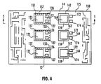
- Fig. 4 illustrates another embodiment of a laminated or rigid-flex multilayer circuit board 150 substantially similar to board 10 illustrated in Fig. 1 wherein board 150 includes a number of mounting areas for a number of electrical devices (not shown).
- Board 150 includes blind vias or recesses 155 having entire footprints 157 located within recess 155.
- Footprint 157 includes pads 126, 127 and a main pad 125. Entire footprints 157 are provided on layer 12.
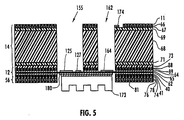
- Board 150 also includes recesses 162 similar to recess 27 (Fig. 1) which have only main pads 164 within recess 162.
- Pads 172 and 174 are provided on a top surface 175 (e.g., layer 14 and, more specifically, layer 66) of board 150.
- a unitary heat sink area 180 is provided opposite recesses 155 and 162 (Fig. 4).
- a single heat sink 173 can be attached or soldered to unitary heat sink area 180. Therefore, single heat sink 173 can be advantageously used to enhance heat dissipation for several electrical devices mounted in recesses 155 and 162.
- heat sink area 180 may be divided into unitary heat sink areas for individual electrical devices.
- one of recesses 155 may be made large enough to include all of footprints 157 and main pads 164.
- thin strips of rigid circuit board material in layer 14 can remain across the single recess (not shown) to provide mechanical strength for mounting heat sinks 92 or 173 and devices 28.
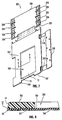
- Motor controller circuit board system 200 includes a module or customer interface board 220 having connector tabs 224, a module or power substrate 260, and a module or a capacitor board 240.
- Power substrate 260 preferably houses IGBT's, SCR's, bipolar transistors, diodes, or other semiconductor switches (not shown) which provide alternating current (AC) power signals for use by a motor (not shown).
- power substrate 260 includes a window 262 (or several alternate size windows) which has only a flexible circuit board layer 12 at a locus between a top surface 265 and a bottom surface 267 ( Figure 8).
- a heat sink (not shown) is mounted on a heat sink area 266 ( Figure 8) of surface 267 and devices, such as device 28, (see Figures 1-5) are attached to surface 265 in window 262.
- System 200 is preferably manufactured from a single flexible circuit layer 12, a rigid circuit board layer 14, and a rigid circuit board layer 56 (Figure 8).
- Layer 12 is preferably continuous with customer interface board 220, power substrate 260, and capacitor circuit board 240.
- Flexible layer 12 provides power bus connectors 242 and 244 between power substrate 260 and capacitor board 240.
- Connectors 242 and 244 preferably house a positive and negative power bus conducting line on each side of connectors 242 and 244 (e.g., layer 12).
- layer 12 provides a connection 222 from substrate 260 to motherboard 220.
- Customer interface board 220 and capacitor circuit board 240 are preferably disposed at a 90° angle with respect to substrate 260 as shown in Figure 6.
- a heat sink (not shown) is preferably attached to surface 267 (e.g., on the same side of substrate 260 from which board 220 and capacitor board 240 extend). This advantageous orientation of system 200 provides superior heat dissipation in a compact package.
- the sides of board 10 or module 260 on which heat sinks 92 or 173 and devices 28 are attached can be switched.
- circuit board system 200 allows high power connections to be made between customer interface board 220, board 240 and substrate 260 without the use of bulky, unreliable and expensive connectors for interconnecting board 220, board 240, and substrate 260. Further, the flexibility associated with flexible layer 12 allows customer interface board 220, board 240 and substrate 260 to be manipulated for various mechanical packages and eases manufacture of circuit board system 200.
- the use of connections between board 220, board 240 and substrate 260 via flexible layer 12 reduces the use of external wires and connectors and hence, the parasitic inductance associated with the interconnection of circuit boards. Therefore, circuit board system 200 provides an advantageous compact structure for a motor controller which is not prone to parasitic inductance problems. Additionally, this use of layer 12 for connections dramatically reduces creepage and clearance distance concerns due to the high voltages present. Furthermore, layer 12 connections provide for impedance control and ground planes in logic signal interconnect areas of system 200.
- an enlarged cross sectional view of a portion of system shows layers 12, 14 and 56 discussed in greater detail with reference to Figures 1-3.
- the thin flexible layer 12 allows superior heat transfer from surface 265 to surface 267 of substrate 260.
- Board 260 preferably includes heat sink area 266 on bottom surface 267 of layer 12.
- window 262 or area 266 can be configured to have rigid strips (not shown) of layer 14 or layer 56 provided in a matrix across window 262 or area 266. The rigid strips provides superior mechanical strength for system 200 at window 262 or area 266.
Landscapes
- Engineering & Computer Science (AREA)
- Microelectronics & Electronic Packaging (AREA)
- Physics & Mathematics (AREA)
- Thermal Sciences (AREA)
- Production Of Multi-Layered Print Wiring Board (AREA)
- Structure Of Printed Boards (AREA)
Applications Claiming Priority (2)
| Application Number | Priority Date | Filing Date | Title |
|---|---|---|---|
| US537216 | 1995-09-29 | ||
| US08/537,216 US5616888A (en) | 1995-09-29 | 1995-09-29 | Rigid-flex circuit board having a window for an insulated mounting area |
Publications (3)
| Publication Number | Publication Date |
|---|---|
| EP0766505A2 true EP0766505A2 (de) | 1997-04-02 |
| EP0766505A3 EP0766505A3 (de) | 1998-12-23 |
| EP0766505B1 EP0766505B1 (de) | 2004-03-31 |
Family
ID=24141719
Family Applications (1)
| Application Number | Title | Priority Date | Filing Date |
|---|---|---|---|
| EP96115348A Expired - Lifetime EP0766505B1 (de) | 1995-09-29 | 1996-09-25 | Starre-flexible Leiterplatte mit einer Öffnung für einen isolierten Montierungsbereich |
Country Status (3)
| Country | Link |
|---|---|
| US (1) | US5616888A (de) |
| EP (1) | EP0766505B1 (de) |
| DE (1) | DE69632003T2 (de) |
Cited By (2)
| Publication number | Priority date | Publication date | Assignee | Title |
|---|---|---|---|---|
| EP0888036A1 (de) * | 1997-06-27 | 1998-12-30 | Samsung Electronics Co., Ltd. | LCD Anordnung mit reduzierter Dicke und Verfahren zum Zusammenbauen |
| US6019522A (en) * | 1997-02-24 | 2000-02-01 | Samsung Electronics Co., Ltd. | Optical part packaging method and collimator assembly method |
Families Citing this family (45)
| Publication number | Priority date | Publication date | Assignee | Title |
|---|---|---|---|---|
| US6321443B1 (en) * | 1995-06-15 | 2001-11-27 | Dyconex Patente Ag | Connection substrate |
| CN1094717C (zh) | 1995-11-16 | 2002-11-20 | 松下电器产业株式会社 | 印刷电路板的安装体 |
| JP2910670B2 (ja) * | 1996-04-12 | 1999-06-23 | 日本電気株式会社 | 半導体実装構造 |
| US5907475A (en) * | 1996-04-16 | 1999-05-25 | Allen-Bradley Company, Llc | Circuit board system having a mounted board and a plurality of mounting boards |
| US5812375A (en) * | 1996-05-06 | 1998-09-22 | Cummins Engine Company, Inc. | Electronic assembly for selective heat sinking and two-sided component attachment |
| SE508138C2 (sv) * | 1996-12-20 | 1998-08-31 | Ericsson Telefon Ab L M | Metod och anordning för anslutning av elektrisk komponent till kretskort |
| US6462976B1 (en) | 1997-02-21 | 2002-10-08 | University Of Arkansas | Conversion of electrical energy from one form to another, and its management through multichip module structures |
| US7144486B1 (en) | 1997-04-30 | 2006-12-05 | Board Of Trustees Of The University Of Arkansas | Multilayer microcavity devices and methods |
| US7169272B2 (en) * | 1997-04-30 | 2007-01-30 | Board Of Trustees Of The University Of Arkansas | Microfabricated recessed disk microelectrodes: characterization in static and convective solutions |
| US6147869A (en) * | 1997-11-24 | 2000-11-14 | International Rectifier Corp. | Adaptable planar module |
| US6212086B1 (en) * | 1998-05-22 | 2001-04-03 | Intel Corporation | Packaging of a DC-to-DC converter |
| US6674163B1 (en) * | 1998-08-18 | 2004-01-06 | Oki Electric Industry Co., Ltd. | Package structure for a semiconductor device |
| JP3602968B2 (ja) * | 1998-08-18 | 2004-12-15 | 沖電気工業株式会社 | 半導体装置およびその基板接続構造 |
| KR100278609B1 (ko) * | 1998-10-08 | 2001-01-15 | 윤종용 | 인쇄회로기판 |
| US6225571B1 (en) * | 1999-02-19 | 2001-05-01 | Lucent Technologies Inc. | Heatsink with high thermal conductivity dielectric |
| US7456028B2 (en) | 2000-10-16 | 2008-11-25 | Board Of Trustees Of The University Of Arkansas, N.A. | Electrochemical method for detecting water born pathogens |
| US6887714B2 (en) | 2000-10-16 | 2005-05-03 | Board Of Trustees Of The University Of Arkansas, N.A. | Microvolume immunoabsorbant assays with amplified electrochemical detection |
| US7348183B2 (en) * | 2000-10-16 | 2008-03-25 | Board Of Trustees Of The University Of Arkansas | Self-contained microelectrochemical bioassay platforms and methods |
| JP3817453B2 (ja) * | 2001-09-25 | 2006-09-06 | 新光電気工業株式会社 | 半導体装置 |
| JP4492280B2 (ja) * | 2004-09-29 | 2010-06-30 | 日立電線株式会社 | 電子部品の実装構造及びそれを用いた光トランシーバ |
| US8624129B2 (en) * | 2006-01-12 | 2014-01-07 | Samsung Electronics Co., Ltd. | Method of attaching a high power surface mount transistor to a printed circuit board |
| US7176707B1 (en) | 2006-02-23 | 2007-02-13 | Lockheed Martin Corporation | Back side component placement and bonding |
| US7772501B2 (en) * | 2006-04-25 | 2010-08-10 | Molex Incorporated | Flexible printed circuit board |
| KR100754080B1 (ko) | 2006-07-13 | 2007-08-31 | 삼성전기주식회사 | 리지드-플렉서블 인쇄회로기판 및 그 제조방법 |
| US7903417B2 (en) * | 2006-10-10 | 2011-03-08 | Deere & Company | Electrical circuit assembly for high-power electronics |
| US20080084671A1 (en) * | 2006-10-10 | 2008-04-10 | Ronnie Dean Stahlhut | Electrical circuit assembly for high-power electronics |
| US7982135B2 (en) * | 2006-10-30 | 2011-07-19 | Ibiden Co., Ltd. | Flex-rigid wiring board and method of manufacturing the same |
| JP5273922B2 (ja) * | 2006-12-28 | 2013-08-28 | 株式会社アライドマテリアル | 放熱部材および半導体装置 |
| US7808788B2 (en) * | 2007-06-29 | 2010-10-05 | Delphi Technologies, Inc. | Multi-layer electrically isolated thermal conduction structure for a circuit board assembly |
| TWI377653B (en) * | 2009-02-16 | 2012-11-21 | Unimicron Technology Corp | Package substrate strucutre with cavity and method for making the same |
| US8897023B2 (en) * | 2009-05-15 | 2014-11-25 | Hamilton Sundstrand Corporation | Motor controller assembly with capacitor thermal isolation |
| TW201127228A (en) * | 2010-01-22 | 2011-08-01 | Ibiden Co Ltd | Flex-rigid wiring board and method for manufacturing the same |
| TW201130405A (en) * | 2010-02-23 | 2011-09-01 | Ibiden Co Ltd | Flex-rigid wiring board and method for manufacturing the same |
| US8683681B2 (en) * | 2010-12-07 | 2014-04-01 | Raytheon Company | Room temperature low contact pressure method |
| US9393263B2 (en) | 2011-06-03 | 2016-07-19 | Allergan, Inc. | Dermal filler compositions including antioxidants |
| KR101443967B1 (ko) * | 2012-10-22 | 2014-09-23 | 삼성전기주식회사 | 방열 기판 및 방열 기판 제조 방법 |
| CN103118489B (zh) * | 2013-01-24 | 2015-12-23 | 宁波舜宇光电信息有限公司 | 一种下沉式软硬结合板及其制造方法 |
| ITMI20130520A1 (it) * | 2013-04-05 | 2014-10-06 | St Microelectronics Srl | Realizzazione di un dissipatore di calore tramite saldatura ad onda |
| EP3496523A1 (de) | 2013-09-23 | 2019-06-12 | Coriant Operations, Inc. | Federclip zur fixierung eines kühlkörpers auf einem sfp/xfp-käfig |
| TWI611740B (zh) * | 2015-02-05 | 2018-01-11 | 頎邦科技股份有限公司 | 可撓性基板 |
| CN106793478A (zh) * | 2017-03-31 | 2017-05-31 | 三禾电器(福建)有限公司 | 一种带有窗口的电路板 |
| CN112492777B (zh) * | 2019-09-12 | 2022-05-27 | 宏启胜精密电子(秦皇岛)有限公司 | 电路板及其制作方法 |
| KR102815912B1 (ko) * | 2019-12-12 | 2025-06-04 | 삼성전기주식회사 | 인쇄회로기판 |
| US12324093B2 (en) * | 2021-06-04 | 2025-06-03 | Steering Solutions Ip Holding Corporation | Single circuit board assembly with logic and power components |
| CN120224573B (zh) * | 2025-05-28 | 2025-07-25 | 深圳市实锐泰科技有限公司 | 一种新能源汽车用高涨缩柔性电路板的制作方法 |
Family Cites Families (13)
| Publication number | Priority date | Publication date | Assignee | Title |
|---|---|---|---|---|
| US3760090A (en) * | 1971-08-19 | 1973-09-18 | Globe Union Inc | Electronic circuit package and method for making same |
| JPS58446U (ja) * | 1981-06-25 | 1983-01-05 | 富士通株式会社 | 混成集積回路装置 |
| US4630172A (en) * | 1983-03-09 | 1986-12-16 | Printed Circuits International | Semiconductor chip carrier package with a heat sink |
| US4861272A (en) * | 1988-03-31 | 1989-08-29 | E. I. Du Pont De Nemours And Company | Impedance controlled connector interface |
| EP0346061A3 (de) * | 1988-06-08 | 1991-04-03 | Fujitsu Limited | Integrierte Schaltungsanordnung mit einer verbesserten Packungsstruktur |
| JPH0650790B2 (ja) * | 1989-01-20 | 1994-06-29 | 三菱マテリアル株式会社 | 混成集積回路およびその製造方法 |
| JPH02201945A (ja) * | 1989-01-30 | 1990-08-10 | Nec Corp | 表面実装型半導体装置 |
| US5045642A (en) * | 1989-04-20 | 1991-09-03 | Satosen, Co., Ltd. | Printed wiring boards with superposed copper foils cores |
| US5306874A (en) * | 1991-07-12 | 1994-04-26 | W.I.T. Inc. | Electrical interconnect and method of its manufacture |
| JPH05160540A (ja) * | 1991-12-04 | 1993-06-25 | Seiko Epson Corp | 回路基板ユニット |
| JPH05327166A (ja) * | 1992-05-26 | 1993-12-10 | Hitachi Ltd | 電子部品実装方法 |
| JPH06216492A (ja) * | 1993-01-21 | 1994-08-05 | Hitachi Ltd | 電子装置 |
| US5412538A (en) * | 1993-07-19 | 1995-05-02 | Cordata, Inc. | Space-saving memory module |
-
1995
- 1995-09-29 US US08/537,216 patent/US5616888A/en not_active Expired - Lifetime
-
1996
- 1996-09-25 EP EP96115348A patent/EP0766505B1/de not_active Expired - Lifetime
- 1996-09-25 DE DE1996632003 patent/DE69632003T2/de not_active Expired - Lifetime
Cited By (2)
| Publication number | Priority date | Publication date | Assignee | Title |
|---|---|---|---|---|
| US6019522A (en) * | 1997-02-24 | 2000-02-01 | Samsung Electronics Co., Ltd. | Optical part packaging method and collimator assembly method |
| EP0888036A1 (de) * | 1997-06-27 | 1998-12-30 | Samsung Electronics Co., Ltd. | LCD Anordnung mit reduzierter Dicke und Verfahren zum Zusammenbauen |
Also Published As
| Publication number | Publication date |
|---|---|
| EP0766505B1 (de) | 2004-03-31 |
| EP0766505A3 (de) | 1998-12-23 |
| DE69632003D1 (de) | 2004-05-06 |
| US5616888A (en) | 1997-04-01 |
| DE69632003T2 (de) | 2004-11-18 |
Similar Documents
| Publication | Publication Date | Title |
|---|---|---|
| US5616888A (en) | Rigid-flex circuit board having a window for an insulated mounting area | |
| US6029343A (en) | Insulated surface mount circuit board construction | |
| EP0766504B1 (de) | Drahtloses Leiterplattensystem für einen Motorregler | |
| US6200407B1 (en) | Method of making a multilayer circuit board having a window exposing an enhanced conductive layer for use as an insulated mounting area | |
| US4858073A (en) | Metal substrated printed circuit | |
| US5315480A (en) | Conformal heat sink for electronic module | |
| US5641944A (en) | Power substrate with improved thermal characteristics | |
| US7903417B2 (en) | Electrical circuit assembly for high-power electronics | |
| US6108205A (en) | Means and method for mounting electronics | |
| JPH07135376A (ja) | 複合プリント回路板とその製造方法 | |
| EP0092020A2 (de) | Zusammengesetzte Struktur insbesondere zur Benutzung als gedruckte Leiterplatte | |
| CN102017135A (zh) | 带有在多个接触平面中的元器件的基板电路模块 | |
| KR100433685B1 (ko) | 10마력모터제어기용전력트레인분할장치 | |
| EP1060645B1 (de) | Elektrischer leiter mit als flanschen und geätzte rillen geformter oberflächenstruktur | |
| CN113823534B (zh) | 包括嵌入控制电子器件的固态开关器件 | |
| US5835356A (en) | Power substrate module | |
| US5670749A (en) | Multilayer circuit board having a window exposing an enhanced conductive layer for use as an insulated mounting area | |
| AU625196B2 (en) | A method and circuit board for mounting a semiconductor component | |
| GB2471497A (en) | Double sided multi-layer metal substrate PCB with SMD components mounted to top traces and lead wire components mounted to opposite side for heat dissipation | |
| US6483706B2 (en) | Heat dissipation for electronic components | |
| EP1025748B1 (de) | Chipträgerelement und dessen verwendung | |
| US6888218B2 (en) | Embedded capacitor multi-chip modules | |
| EP0804054A1 (de) | Isolierte oberflächenmontierte Leiterplattenkonstruktion | |
| CN115280495A (zh) | 功率模块 | |
| WO2008045430A1 (en) | Electrical circuit assembly for high-power electronics |
Legal Events
| Date | Code | Title | Description |
|---|---|---|---|
| PUAI | Public reference made under article 153(3) epc to a published international application that has entered the european phase |
Free format text: ORIGINAL CODE: 0009012 |
|
| AK | Designated contracting states |
Kind code of ref document: A2 Designated state(s): DE FR GB IT |
|
| PUAL | Search report despatched |
Free format text: ORIGINAL CODE: 0009013 |
|
| AK | Designated contracting states |
Kind code of ref document: A3 Designated state(s): DE FR GB IT |
|
| 17P | Request for examination filed |
Effective date: 19990604 |
|
| 17Q | First examination report despatched |
Effective date: 20021203 |
|
| GRAP | Despatch of communication of intention to grant a patent |
Free format text: ORIGINAL CODE: EPIDOSNIGR1 |
|
| GRAS | Grant fee paid |
Free format text: ORIGINAL CODE: EPIDOSNIGR3 |
|
| GRAA | (expected) grant |
Free format text: ORIGINAL CODE: 0009210 |
|
| RAP1 | Party data changed (applicant data changed or rights of an application transferred) |
Owner name: ROCKWELL AUTOMATION TECHNOLOGIES, INC. |
|
| AK | Designated contracting states |
Kind code of ref document: B1 Designated state(s): DE FR GB IT |
|
| REG | Reference to a national code |
Ref country code: GB Ref legal event code: FG4D |
|
| REF | Corresponds to: |
Ref document number: 69632003 Country of ref document: DE Date of ref document: 20040506 Kind code of ref document: P |
|
| ET | Fr: translation filed | ||
| PLBE | No opposition filed within time limit |
Free format text: ORIGINAL CODE: 0009261 |
|
| STAA | Information on the status of an ep patent application or granted ep patent |
Free format text: STATUS: NO OPPOSITION FILED WITHIN TIME LIMIT |
|
| 26N | No opposition filed |
Effective date: 20050104 |
|
| PGFP | Annual fee paid to national office [announced via postgrant information from national office to epo] |
Ref country code: IT Payment date: 20080926 Year of fee payment: 13 Ref country code: FR Payment date: 20080915 Year of fee payment: 13 |
|
| PGFP | Annual fee paid to national office [announced via postgrant information from national office to epo] |
Ref country code: GB Payment date: 20081001 Year of fee payment: 13 |
|
| PGFP | Annual fee paid to national office [announced via postgrant information from national office to epo] |
Ref country code: DE Payment date: 20090929 Year of fee payment: 14 |
|
| GBPC | Gb: european patent ceased through non-payment of renewal fee |
Effective date: 20090925 |
|
| REG | Reference to a national code |
Ref country code: FR Ref legal event code: ST Effective date: 20100531 |
|
| PG25 | Lapsed in a contracting state [announced via postgrant information from national office to epo] |
Ref country code: FR Free format text: LAPSE BECAUSE OF NON-PAYMENT OF DUE FEES Effective date: 20090930 |
|
| PG25 | Lapsed in a contracting state [announced via postgrant information from national office to epo] |
Ref country code: GB Free format text: LAPSE BECAUSE OF NON-PAYMENT OF DUE FEES Effective date: 20090925 |
|
| PG25 | Lapsed in a contracting state [announced via postgrant information from national office to epo] |
Ref country code: IT Free format text: LAPSE BECAUSE OF NON-PAYMENT OF DUE FEES Effective date: 20090925 |
|
| REG | Reference to a national code |
Ref country code: DE Ref legal event code: R119 Ref document number: 69632003 Country of ref document: DE Effective date: 20110401 |
|
| PG25 | Lapsed in a contracting state [announced via postgrant information from national office to epo] |
Ref country code: DE Free format text: LAPSE BECAUSE OF NON-PAYMENT OF DUE FEES Effective date: 20110401 |