EP0768740A1 - Elément optoélectronique avec couplage de mode codirectionnel - Google Patents
Elément optoélectronique avec couplage de mode codirectionnel Download PDFInfo
- Publication number
- EP0768740A1 EP0768740A1 EP96114847A EP96114847A EP0768740A1 EP 0768740 A1 EP0768740 A1 EP 0768740A1 EP 96114847 A EP96114847 A EP 96114847A EP 96114847 A EP96114847 A EP 96114847A EP 0768740 A1 EP0768740 A1 EP 0768740A1
- Authority
- EP
- European Patent Office
- Prior art keywords
- layer
- modes
- propagation
- waveguide layers
- sections
- Prior art date
- Legal status (The legal status is an assumption and is not a legal conclusion. Google has not performed a legal analysis and makes no representation as to the accuracy of the status listed.)
- Granted
Links
Images


Classifications
-
- G—PHYSICS
- G02—OPTICS
- G02B—OPTICAL ELEMENTS, SYSTEMS OR APPARATUS
- G02B6/00—Light guides; Structural details of arrangements comprising light guides and other optical elements, e.g. couplings
- G02B6/10—Light guides; Structural details of arrangements comprising light guides and other optical elements, e.g. couplings of the optical waveguide type
- G02B6/12—Light guides; Structural details of arrangements comprising light guides and other optical elements, e.g. couplings of the optical waveguide type of the integrated circuit kind
- G02B6/12007—Light guides; Structural details of arrangements comprising light guides and other optical elements, e.g. couplings of the optical waveguide type of the integrated circuit kind forming wavelength selective elements, e.g. multiplexer, demultiplexer
-
- G—PHYSICS
- G02—OPTICS
- G02B—OPTICAL ELEMENTS, SYSTEMS OR APPARATUS
- G02B6/00—Light guides; Structural details of arrangements comprising light guides and other optical elements, e.g. couplings
- G02B6/24—Coupling light guides
- G02B6/42—Coupling light guides with opto-electronic elements
- G02B6/4201—Packages, e.g. shape, construction, internal or external details
- G02B6/4204—Packages, e.g. shape, construction, internal or external details the coupling comprising intermediate optical elements, e.g. lenses, holograms
- G02B6/4215—Packages, e.g. shape, construction, internal or external details the coupling comprising intermediate optical elements, e.g. lenses, holograms the intermediate optical elements being wavelength selective optical elements, e.g. variable wavelength optical modules or wavelength lockers
-
- G—PHYSICS
- G02—OPTICS
- G02F—OPTICAL DEVICES OR ARRANGEMENTS FOR THE CONTROL OF LIGHT BY MODIFICATION OF THE OPTICAL PROPERTIES OF THE MEDIA OF THE ELEMENTS INVOLVED THEREIN; NON-LINEAR OPTICS; FREQUENCY-CHANGING OF LIGHT; OPTICAL LOGIC ELEMENTS; OPTICAL ANALOGUE/DIGITAL CONVERTERS
- G02F1/00—Devices or arrangements for the control of the intensity, colour, phase, polarisation or direction of light arriving from an independent light source, e.g. switching, gating or modulating; Non-linear optics
- G02F1/29—Devices or arrangements for the control of the intensity, colour, phase, polarisation or direction of light arriving from an independent light source, e.g. switching, gating or modulating; Non-linear optics for the control of the position or the direction of light beams, i.e. deflection
- G02F1/31—Digital deflection, i.e. optical switching
- G02F1/313—Digital deflection, i.e. optical switching in an optical waveguide structure
- G02F1/3132—Digital deflection, i.e. optical switching in an optical waveguide structure of directional coupler type
-
- H—ELECTRICITY
- H01—ELECTRIC ELEMENTS
- H01S—DEVICES USING THE PROCESS OF LIGHT AMPLIFICATION BY STIMULATED EMISSION OF RADIATION [LASER] TO AMPLIFY OR GENERATE LIGHT; DEVICES USING STIMULATED EMISSION OF ELECTROMAGNETIC RADIATION IN WAVE RANGES OTHER THAN OPTICAL
- H01S5/00—Semiconductor lasers
- H01S5/10—Construction or shape of the optical resonator, e.g. extended or external cavity, coupled cavities, bent-guide, varying width, thickness or composition of the active region
- H01S5/1028—Coupling to elements in the cavity, e.g. coupling to waveguides adjacent the active region, e.g. forward coupled [DFC] structures
- H01S5/1032—Coupling to elements comprising an optical axis that is not aligned with the optical axis of the active region
-
- G—PHYSICS
- G02—OPTICS
- G02B—OPTICAL ELEMENTS, SYSTEMS OR APPARATUS
- G02B6/00—Light guides; Structural details of arrangements comprising light guides and other optical elements, e.g. couplings
- G02B6/10—Light guides; Structural details of arrangements comprising light guides and other optical elements, e.g. couplings of the optical waveguide type
- G02B6/12—Light guides; Structural details of arrangements comprising light guides and other optical elements, e.g. couplings of the optical waveguide type of the integrated circuit kind
- G02B2006/12083—Constructional arrangements
- G02B2006/12107—Grating
-
- G—PHYSICS
- G02—OPTICS
- G02B—OPTICAL ELEMENTS, SYSTEMS OR APPARATUS
- G02B6/00—Light guides; Structural details of arrangements comprising light guides and other optical elements, e.g. couplings
- G02B6/10—Light guides; Structural details of arrangements comprising light guides and other optical elements, e.g. couplings of the optical waveguide type
- G02B6/12—Light guides; Structural details of arrangements comprising light guides and other optical elements, e.g. couplings of the optical waveguide type of the integrated circuit kind
- G02B2006/12133—Functions
- G02B2006/12147—Coupler
-
- G—PHYSICS
- G02—OPTICS
- G02F—OPTICAL DEVICES OR ARRANGEMENTS FOR THE CONTROL OF LIGHT BY MODIFICATION OF THE OPTICAL PROPERTIES OF THE MEDIA OF THE ELEMENTS INVOLVED THEREIN; NON-LINEAR OPTICS; FREQUENCY-CHANGING OF LIGHT; OPTICAL LOGIC ELEMENTS; OPTICAL ANALOGUE/DIGITAL CONVERTERS
- G02F1/00—Devices or arrangements for the control of the intensity, colour, phase, polarisation or direction of light arriving from an independent light source, e.g. switching, gating or modulating; Non-linear optics
- G02F1/29—Devices or arrangements for the control of the intensity, colour, phase, polarisation or direction of light arriving from an independent light source, e.g. switching, gating or modulating; Non-linear optics for the control of the position or the direction of light beams, i.e. deflection
- G02F1/31—Digital deflection, i.e. optical switching
- G02F1/313—Digital deflection, i.e. optical switching in an optical waveguide structure
- G02F1/3132—Digital deflection, i.e. optical switching in an optical waveguide structure of directional coupler type
- G02F1/3133—Digital deflection, i.e. optical switching in an optical waveguide structure of directional coupler type the optical waveguides being made of semiconducting materials
-
- G—PHYSICS
- G02—OPTICS
- G02F—OPTICAL DEVICES OR ARRANGEMENTS FOR THE CONTROL OF LIGHT BY MODIFICATION OF THE OPTICAL PROPERTIES OF THE MEDIA OF THE ELEMENTS INVOLVED THEREIN; NON-LINEAR OPTICS; FREQUENCY-CHANGING OF LIGHT; OPTICAL LOGIC ELEMENTS; OPTICAL ANALOGUE/DIGITAL CONVERTERS
- G02F1/00—Devices or arrangements for the control of the intensity, colour, phase, polarisation or direction of light arriving from an independent light source, e.g. switching, gating or modulating; Non-linear optics
- G02F1/29—Devices or arrangements for the control of the intensity, colour, phase, polarisation or direction of light arriving from an independent light source, e.g. switching, gating or modulating; Non-linear optics for the control of the position or the direction of light beams, i.e. deflection
- G02F1/31—Digital deflection, i.e. optical switching
- G02F1/313—Digital deflection, i.e. optical switching in an optical waveguide structure
- G02F1/3132—Digital deflection, i.e. optical switching in an optical waveguide structure of directional coupler type
- G02F1/3135—Vertical structure
-
- G—PHYSICS
- G02—OPTICS
- G02F—OPTICAL DEVICES OR ARRANGEMENTS FOR THE CONTROL OF LIGHT BY MODIFICATION OF THE OPTICAL PROPERTIES OF THE MEDIA OF THE ELEMENTS INVOLVED THEREIN; NON-LINEAR OPTICS; FREQUENCY-CHANGING OF LIGHT; OPTICAL LOGIC ELEMENTS; OPTICAL ANALOGUE/DIGITAL CONVERTERS
- G02F2201/00—Constructional arrangements not provided for in groups G02F1/00 - G02F7/00
- G02F2201/30—Constructional arrangements not provided for in groups G02F1/00 - G02F7/00 grating
-
- G—PHYSICS
- G02—OPTICS
- G02F—OPTICAL DEVICES OR ARRANGEMENTS FOR THE CONTROL OF LIGHT BY MODIFICATION OF THE OPTICAL PROPERTIES OF THE MEDIA OF THE ELEMENTS INVOLVED THEREIN; NON-LINEAR OPTICS; FREQUENCY-CHANGING OF LIGHT; OPTICAL LOGIC ELEMENTS; OPTICAL ANALOGUE/DIGITAL CONVERTERS
- G02F2201/00—Constructional arrangements not provided for in groups G02F1/00 - G02F7/00
- G02F2201/30—Constructional arrangements not provided for in groups G02F1/00 - G02F7/00 grating
- G02F2201/302—Constructional arrangements not provided for in groups G02F1/00 - G02F7/00 grating grating coupler
-
- H—ELECTRICITY
- H01—ELECTRIC ELEMENTS
- H01S—DEVICES USING THE PROCESS OF LIGHT AMPLIFICATION BY STIMULATED EMISSION OF RADIATION [LASER] TO AMPLIFY OR GENERATE LIGHT; DEVICES USING STIMULATED EMISSION OF ELECTROMAGNETIC RADIATION IN WAVE RANGES OTHER THAN OPTICAL
- H01S5/00—Semiconductor lasers
- H01S5/06—Arrangements for controlling the laser output parameters, e.g. by operating on the active medium
- H01S5/062—Arrangements for controlling the laser output parameters, e.g. by operating on the active medium by varying the potential of the electrodes
- H01S5/06203—Transistor-type lasers
- H01S5/06206—Controlling the frequency of the radiation, e.g. tunable twin-guide lasers [TTG]
-
- H—ELECTRICITY
- H01—ELECTRIC ELEMENTS
- H01S—DEVICES USING THE PROCESS OF LIGHT AMPLIFICATION BY STIMULATED EMISSION OF RADIATION [LASER] TO AMPLIFY OR GENERATE LIGHT; DEVICES USING STIMULATED EMISSION OF ELECTROMAGNETIC RADIATION IN WAVE RANGES OTHER THAN OPTICAL
- H01S5/00—Semiconductor lasers
- H01S5/10—Construction or shape of the optical resonator, e.g. extended or external cavity, coupled cavities, bent-guide, varying width, thickness or composition of the active region
- H01S5/1028—Coupling to elements in the cavity, e.g. coupling to waveguides adjacent the active region, e.g. forward coupled [DFC] structures
- H01S5/1032—Coupling to elements comprising an optical axis that is not aligned with the optical axis of the active region
- H01S5/1035—Forward coupled structures [DFC]
Definitions
- Electronically tunable integrated laser diodes with a large tuning range, ie greater than approx. 1% of the wavelength, are key components for multiple applications in optical communication technology.
- those with codirectional mode coupling are advantageous since they only require a single tuning current.
- Such laser diodes are e.g. B. described in the publications by I. Kim et al .: Broadly tunable vertical-coupler filtered tensile-strained InGaAs / InGaAsP multiple quantum well laser "in Appl. Phys. Lett. 64 , 2764 to 2766 (1994) and by M.-C. Amann et al .: Widley Tunable Distributed Forward Coupled (DFC) Laser "in Electr. Lett. 29 , 793 to 794 (1993).
- DFC Distributed Forward Coupled
- EP 0 552 390 A1 describes a tunable laser diode in which codirectional mode coupling is brought about by a periodically interrupted absorber layer arranged parallel to two waveguide layers. At the longitudinal edges of the individual sections of this absorber layer, cracks occur in the real part of the effective refractive index in the waveguide layers. The internal back reflections therefore occur periodically in this laser diode.
- EP 0 411 816 A2 describes the production of waveguide tapers which taper in the vertical direction.
- the waveguide is formed by a plurality of InGaAsP layers with InP etch stop layers in between.
- the taper is produced by gradually etching this layer structure.
- the object of the present invention is to provide an optoelectronic component with codirectional mode coupling, in which undesired internal back reflections of the guided modes are prevented as far as possible.
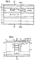
- FIG. 1 shows a typical arrangement of two waveguide layers WG1, WG2 and a periodically structured layer ⁇ n, with which the codirectional coupling is brought about.
- FIG. 1a the side view is shown
- FIG. 1b the view in the viewing direction shown in FIG. 1a is shown.
- the modes carried in the waveguide layers with WG1, WG2 are coupled at a wavelength which is equal to the product of the period ⁇ and the difference of the real part of the effective refractive index of the two fashions.
- FIG. 2 A section from Figure 1b is drawn in Figure 2.
- the modes propagate in the direction of the z-axis.
- a portion of the periodically structured layer ⁇ n is drawn on the right side, the edge of which includes the angle Rand with the perpendicular to the longitudinal direction of the waveguide in the layer plane. This results in a path length ⁇ z on which the real part of the effective refractive index undergoes a continuous change.
- the width of the layer ⁇ n corresponds to the width W of the waveguide layers WG1, WG2.
- the codirectionally coupled modes R, S are shown on the left side by the amplitudes of their field strengths. With this arrangement, the total reflection results as an integral along the distance ⁇ z.
- the components of the reflection are extinguished by strong destructive interference during the integration.
- the codirectional coupling is also reduced when the refractive indices change continuously.
- this influence is about two orders of magnitude smaller, since it is not the transit time or phase position of the individual transverse modes R or S that is decisive here, but rather the transit time or phase difference of the modes when the distance ⁇ z is traveled.
- ⁇ z there is therefore a large range of values for ⁇ z, within which destructive interference of reflection and reduction of total reflection occurs on the one hand, but on the other hand does not yet noticeably impair the codirectional mode coupling becomes.
- ⁇ z there is therefore a range between half the wavelength of the laser in vacuum, divided by the mean effective refractive index of the transverse modes R and S, and the quarter wavelength of the laser in vacuum, divided by the difference between the effective refractive indices of the modes.
- Typical values are e.g. B. 1.55 microns for the vacuum wavelength, 3.3 for the mean effective refractive index and 0.1 for the difference between the effective refractive indices of the modes in an InGaAsP laser diode.
- the intermediate layer 6 is opposite, that is to say doped n-conductively.
- the proportions of the absorber layer of length S with the subsequent interruption of the Length T together form a period P of the periodic structuring.
- Contacts 1, 9 and 11 are used for the electrical connection.
- the lateral cladding layer 15 is doped n-conductively and establishes the conductive connection between the intermediate layer 6 and the lateral contact 11 via a further intermediate layer 12, an etching stop layer 13 and a contact layer 14 doped with a high n-conductivity.
- the currents I a for generating the laser radiation and I t for tuning are also shown.
- This laser diode has the structure of a TTG laser diode (Tunable Twin Guide), as described in DE 92 100 886.
- the respective sections of the absorber layer 4 are beveled here according to the invention in accordance with FIG. 1b or FIG. 2, so that the interfaces or edges of the portions of the absorber layer 4 are obliquely oblique to the longitudinal direction of the waveguide when viewed from above.
- the interfaces of the layer ⁇ n are aligned at an angle to the direction of propagation of the modes which is different from a right angle perpendicular to the layer plane.
- the z-axis see Figure 5b
- a normal close an angle of such an interface the vertical projection of which in a plane perpendicular to the layer plane is different from 0 ° or 180 °.
- the interfaces of the layer ⁇ n are oriented at an angle which is different in the layer plane from a right angle to the direction of propagation of the modes, ie the z-axis (see FIG.
- FIGS. 1 and 5 can thus be combined with one another.
- Said interface does not have to be a flat surface, but can e.g. B. curved or rounded at the edges.
- the boundary shown in Figure 1b in supervision of a portion of the layer ⁇ n need not be straight as shown, but can be rounded in a suitable manner or z. B. be s-shaped.
- One possible production method takes advantage of the different growth rate of the semiconductor materials that make up the mixed crystal, which depends on the width of the mask opening.
- epitaxial growth in the area of the slit-shaped opening gives a higher growth rate, which steadily decreases towards the outside up to the growth rate on unmasked areas.
- the grown layer receives a gradation in the composition of the semiconductor mixed crystal in the area of the expansion of the mask opening.
- the embodiment of FIG. 5 can, as stated, be designed in such a way that the periodically structured layer ⁇ n comprises a plurality of layers which are arranged vertically one above the other and form the layer ⁇ n in their entirety. These layers can have different material compositions and can also be separated from one another by thin etching stop layers.
- Such a multilayered layer structure makes it possible not only to obtain the changes in the vertical dimension occurring in the longitudinal direction of the waveguide by etching the tapered portions of the layer ⁇ n in stages, but also to obtain multiply graduated changes in the refractive index by the gradual arrangement of layers with different material compositions .
- a combination of the laterally varying dimension of the layer ⁇ n as in the exemplary embodiment in FIG. 1 with a varying material composition in the longitudinal direction of the waveguide is also possible.
- the principle described here on the basis of the exemplary embodiments can be applied at all points in a component with a codirectional coupling at which discontinuous changes in the effective refractive index are to be avoided. That can e.g. B. be the case with transitions between active and passive areas of the component.
- An embodiment as described above for each portion of the periodically structured layer ( ⁇ n or 4) can, for. B. only be present at the edges of a grid provided for the coupling. The existing edges of the grid in the direction of propagation of the modes are then z. B. arranged obliquely to this direction of propagation. The discontinuities in the refractive index provided and desired along the grating remain unaffected.
- portions of a compensation layer can be provided which keep the real portion of the effective refractive index constant, if possible.
- the means according to the invention for the continuous adjustment of the refractive index can then in this compensation layer or possibly a further layer which, for. B. is arranged vertically to the periodically structured layer ⁇ n.
Landscapes
- Physics & Mathematics (AREA)
- General Physics & Mathematics (AREA)
- Optics & Photonics (AREA)
- Nonlinear Science (AREA)
- Engineering & Computer Science (AREA)
- Microelectronics & Electronic Packaging (AREA)
- Condensed Matter Physics & Semiconductors (AREA)
- Electromagnetism (AREA)
- Optical Integrated Circuits (AREA)
- Optical Couplings Of Light Guides (AREA)
- Semiconductor Lasers (AREA)
Applications Claiming Priority (2)
| Application Number | Priority Date | Filing Date | Title |
|---|---|---|---|
| DE19538232A DE19538232A1 (de) | 1995-10-13 | 1995-10-13 | Optoelektronisches Bauelement mit kodirektionaler Modenkopplung |
| DE19538232 | 1995-10-13 |
Publications (2)
| Publication Number | Publication Date |
|---|---|
| EP0768740A1 true EP0768740A1 (fr) | 1997-04-16 |
| EP0768740B1 EP0768740B1 (fr) | 1999-05-12 |
Family
ID=7774822
Family Applications (1)
| Application Number | Title | Priority Date | Filing Date |
|---|---|---|---|
| EP96114847A Expired - Lifetime EP0768740B1 (fr) | 1995-10-13 | 1996-09-16 | Elément optoélectronique avec couplage de mode codirectionnel |
Country Status (5)
| Country | Link |
|---|---|
| US (1) | US5784398A (fr) |
| EP (1) | EP0768740B1 (fr) |
| JP (1) | JPH09129955A (fr) |
| DE (2) | DE19538232A1 (fr) |
| TW (1) | TW373359B (fr) |
Families Citing this family (3)
| Publication number | Priority date | Publication date | Assignee | Title |
|---|---|---|---|---|
| US6577658B1 (en) * | 1999-09-20 | 2003-06-10 | E20 Corporation, Inc. | Method and apparatus for planar index guided vertical cavity surface emitting lasers |
| NL1015714C2 (nl) * | 2000-07-14 | 2002-01-15 | Dsm Nv | Werkwijze voor het kristalliseren van enantiomeer verrijkt 2-acetylthio-3-fenylpropaanzuur. |
| US6947463B2 (en) * | 2000-10-23 | 2005-09-20 | The Furukawa Electric Co., Ltd. | Semiconductor laser device for use in a laser module |
Citations (1)
| Publication number | Priority date | Publication date | Assignee | Title |
|---|---|---|---|---|
| EP0552390A1 (fr) * | 1992-01-20 | 1993-07-28 | Siemens Aktiengesellschaft | Diode laser accordable |
Family Cites Families (7)
| Publication number | Priority date | Publication date | Assignee | Title |
|---|---|---|---|---|
| JPH088394B2 (ja) * | 1989-06-30 | 1996-01-29 | 三菱電機株式会社 | 半導体レーザおよびその製造方法 |
| CA2020246C (fr) * | 1989-08-03 | 1994-02-01 | Thomas L. Koch | Guides d'ondes profiles a semiconducteur et methode de fabrication de ces guides |
| US4932032A (en) * | 1989-08-03 | 1990-06-05 | At&T Bell Laboratories | Tapered semiconductor waveguides |
| US4944838A (en) * | 1989-08-03 | 1990-07-31 | At&T Bell Laboratories | Method of making tapered semiconductor waveguides |
| US5208824A (en) * | 1991-12-12 | 1993-05-04 | At&T Bell Laboratories | Article comprising a DFB semiconductor laser |
| US5539766A (en) * | 1993-08-19 | 1996-07-23 | Matsushita Electric Industrial Co., Ltd. | Distributed feedback semiconductor laser |
| US5452318A (en) * | 1993-12-16 | 1995-09-19 | Northern Telecom Limited | Gain-coupled DFB laser with index coupling compensation |
-
1995
- 1995-10-13 DE DE19538232A patent/DE19538232A1/de not_active Withdrawn
-
1996
- 1996-09-07 TW TW085110967A patent/TW373359B/zh active
- 1996-09-16 EP EP96114847A patent/EP0768740B1/fr not_active Expired - Lifetime
- 1996-09-16 DE DE59601864T patent/DE59601864D1/de not_active Expired - Fee Related
- 1996-10-09 JP JP8285850A patent/JPH09129955A/ja active Pending
- 1996-10-15 US US08/731,451 patent/US5784398A/en not_active Expired - Lifetime
Patent Citations (1)
| Publication number | Priority date | Publication date | Assignee | Title |
|---|---|---|---|---|
| EP0552390A1 (fr) * | 1992-01-20 | 1993-07-28 | Siemens Aktiengesellschaft | Diode laser accordable |
Non-Patent Citations (2)
| Title |
|---|
| AMANN M -C ET AL: "DISTRIBUTED FORWARD COUPLED (DFC) LASER", I.E.E.E. JOURNAL OF SELECTED TOPICS IN QUANTUM ELECTRONICS, vol. 1, no. 2, 1 June 1995 (1995-06-01), pages 387 - 395, XP000521102 * |
| AMANN M -C ET AL: "WIDELY TUNABLE LASER DIODES WITH TAPERED INDEX PERTURBATIONS FOR REDUCED INTERNAL REFLECTIONS AND IMPROVED WAVELENGTH ACCESS", ELECTRONICS LETTERS, vol. 32, no. 3, 1 February 1996 (1996-02-01), pages 221/222, XP000554952 * |
Also Published As
| Publication number | Publication date |
|---|---|
| DE19538232A1 (de) | 1997-04-17 |
| US5784398A (en) | 1998-07-21 |
| EP0768740B1 (fr) | 1999-05-12 |
| JPH09129955A (ja) | 1997-05-16 |
| DE59601864D1 (de) | 1999-06-17 |
| TW373359B (en) | 1999-11-01 |
Similar Documents
| Publication | Publication Date | Title |
|---|---|---|
| EP0418705B1 (fr) | Laser à semi-conducteur interférométrique | |
| DE69505250T2 (de) | Spannungskompensierte multiquantumwell-laserstruktur | |
| DE4328777B4 (de) | Optische Filtervorrichtung | |
| DE69104429T2 (de) | Optisches Halbleiterbauelement. | |
| DE102009019996B4 (de) | DFB Laserdiode mit lateraler Kopplung für große Ausgangsleistungen | |
| DE69209016T2 (de) | Gegenstand der einen DFB-Halbleiterlaser enthält | |
| DE69505064T2 (de) | Wellenlängenabstimmbarer Halbleiterlaser | |
| DE3781931T2 (de) | Halbleiterlaser mit verteilter rueckkopplung und kontinuierlich abstimmbarer wellenlaenge. | |
| DE69612104T2 (de) | Optische filter | |
| EP0849847B1 (fr) | Elément optoélectronique avec une structure MQW | |
| DE69111197T2 (de) | Abstimmbarer Halbleiterlaser mit verteilter Rückkopplung. | |
| DE69129181T2 (de) | Optische Halbleitervorrichtung | |
| DE3689188T2 (de) | Halbleiterlaser. | |
| DE19633373A1 (de) | Aufbau eines in der Wellenlänge abstimmbaren Lasers | |
| DE68913934T2 (de) | Verstimmbarer Halbleiterdiodenlaser mit verteilter Reflexion und Verfahren zum Herstellen eines derartigen Halbleiterdiodenlasers. | |
| DE69404107T2 (de) | Polarisationsunabhängiger optischer Halbleiterverstärker | |
| DE69011921T2 (de) | Halbleiterlaser mit veränderbarer Emissionswellenlänge und selektives Wellenlängenfitter und Verfahren zum Betrieb derselben. | |
| DE69029207T2 (de) | Optische Halbleitervorrichtung | |
| DE69101693T2 (de) | Halbleiter-Wellenlängenwandler. | |
| DE69203784T2 (de) | Gewinngekoppelter Halbleiterlaser mit verteilter Rückkoppelung. | |
| DE69203418T2 (de) | Halbleiter-Vorrichtung und Methode zu deren Herstellung. | |
| DE69116743T2 (de) | Phasenverschobener Halbleiterlaser mit verteilter Rückkoppelung | |
| EP0552390B1 (fr) | Diode laser accordable | |
| EP0976183B1 (fr) | Composant optoelectronique accordable en longueur d'onde | |
| DE3875768T2 (de) | Halbleiterlaser mit verteilter rueckkopplung. |
Legal Events
| Date | Code | Title | Description |
|---|---|---|---|
| PUAI | Public reference made under article 153(3) epc to a published international application that has entered the european phase |
Free format text: ORIGINAL CODE: 0009012 |
|
| AK | Designated contracting states |
Kind code of ref document: A1 Designated state(s): DE FR GB |
|
| 17P | Request for examination filed |
Effective date: 19970505 |
|
| GRAG | Despatch of communication of intention to grant |
Free format text: ORIGINAL CODE: EPIDOS AGRA |
|
| GRAG | Despatch of communication of intention to grant |
Free format text: ORIGINAL CODE: EPIDOS AGRA |
|
| GRAH | Despatch of communication of intention to grant a patent |
Free format text: ORIGINAL CODE: EPIDOS IGRA |
|
| 17Q | First examination report despatched |
Effective date: 19981105 |
|
| GRAH | Despatch of communication of intention to grant a patent |
Free format text: ORIGINAL CODE: EPIDOS IGRA |
|
| GRAA | (expected) grant |
Free format text: ORIGINAL CODE: 0009210 |
|
| AK | Designated contracting states |
Kind code of ref document: B1 Designated state(s): DE FR GB |
|
| REF | Corresponds to: |
Ref document number: 59601864 Country of ref document: DE Date of ref document: 19990617 |
|
| ET | Fr: translation filed | ||
| GBT | Gb: translation of ep patent filed (gb section 77(6)(a)/1977) |
Effective date: 19990708 |
|
| PLBE | No opposition filed within time limit |
Free format text: ORIGINAL CODE: 0009261 |
|
| STAA | Information on the status of an ep patent application or granted ep patent |
Free format text: STATUS: NO OPPOSITION FILED WITHIN TIME LIMIT |
|
| 26N | No opposition filed | ||
| REG | Reference to a national code |
Ref country code: GB Ref legal event code: IF02 |
|
| PGFP | Annual fee paid to national office [announced via postgrant information from national office to epo] |
Ref country code: FR Payment date: 20050823 Year of fee payment: 10 |
|
| PGFP | Annual fee paid to national office [announced via postgrant information from national office to epo] |
Ref country code: GB Payment date: 20050905 Year of fee payment: 10 |
|
| PGFP | Annual fee paid to national office [announced via postgrant information from national office to epo] |
Ref country code: DE Payment date: 20051115 Year of fee payment: 10 |
|
| PG25 | Lapsed in a contracting state [announced via postgrant information from national office to epo] |
Ref country code: DE Free format text: LAPSE BECAUSE OF NON-PAYMENT OF DUE FEES Effective date: 20070403 |
|
| GBPC | Gb: european patent ceased through non-payment of renewal fee |
Effective date: 20060916 |
|
| REG | Reference to a national code |
Ref country code: FR Ref legal event code: ST Effective date: 20070531 |
|
| PG25 | Lapsed in a contracting state [announced via postgrant information from national office to epo] |
Ref country code: GB Free format text: LAPSE BECAUSE OF NON-PAYMENT OF DUE FEES Effective date: 20060916 |
|
| PG25 | Lapsed in a contracting state [announced via postgrant information from national office to epo] |
Ref country code: FR Free format text: LAPSE BECAUSE OF NON-PAYMENT OF DUE FEES Effective date: 20061002 |