EP0768813A2 - Panneaux à circuit imprimé - Google Patents
Panneaux à circuit imprimé Download PDFInfo
- Publication number
- EP0768813A2 EP0768813A2 EP96402167A EP96402167A EP0768813A2 EP 0768813 A2 EP0768813 A2 EP 0768813A2 EP 96402167 A EP96402167 A EP 96402167A EP 96402167 A EP96402167 A EP 96402167A EP 0768813 A2 EP0768813 A2 EP 0768813A2
- Authority
- EP
- European Patent Office
- Prior art keywords
- wiring pattern
- printed circuit
- circuit board
- openings
- opening
- Prior art date
- Legal status (The legal status is an assumption and is not a legal conclusion. Google has not performed a legal analysis and makes no representation as to the accuracy of the status listed.)
- Granted
Links
- 230000000149 penetrating effect Effects 0.000 claims description 5
- 239000004020 conductor Substances 0.000 claims 3
- 229910000679 solder Inorganic materials 0.000 abstract description 20
- RYGMFSIKBFXOCR-UHFFFAOYSA-N Copper Chemical compound [Cu] RYGMFSIKBFXOCR-UHFFFAOYSA-N 0.000 description 14
- 239000011889 copper foil Substances 0.000 description 8
- 229910052802 copper Inorganic materials 0.000 description 6
- 239000010949 copper Substances 0.000 description 6
- 238000007598 dipping method Methods 0.000 description 2
- 238000005530 etching Methods 0.000 description 2
- 239000002184 metal Substances 0.000 description 2
- 229910052751 metal Inorganic materials 0.000 description 2
- 238000004080 punching Methods 0.000 description 2
- 230000000694 effects Effects 0.000 description 1
- 239000003822 epoxy resin Substances 0.000 description 1
- 239000004744 fabric Substances 0.000 description 1
- 239000011521 glass Substances 0.000 description 1
- 239000003365 glass fiber Substances 0.000 description 1
- 229920000647 polyepoxide Polymers 0.000 description 1
Images

Classifications
-
- H—ELECTRICITY
- H05—ELECTRIC TECHNIQUES NOT OTHERWISE PROVIDED FOR
- H05K—PRINTED CIRCUITS; CASINGS OR CONSTRUCTIONAL DETAILS OF ELECTRIC APPARATUS; MANUFACTURE OF ASSEMBLAGES OF ELECTRICAL COMPONENTS
- H05K1/00—Printed circuits
- H05K1/02—Details
- H05K1/0213—Electrical arrangements not otherwise provided for
- H05K1/0263—High current adaptations, e.g. printed high current conductors or using auxiliary non-printed means; Fine and coarse circuit patterns on one circuit board
- H05K1/0265—High current adaptations, e.g. printed high current conductors or using auxiliary non-printed means; Fine and coarse circuit patterns on one circuit board characterized by the lay-out of or details of the printed conductors, e.g. reinforced conductors, redundant conductors, conductors having different cross-sections
-
- H—ELECTRICITY
- H05—ELECTRIC TECHNIQUES NOT OTHERWISE PROVIDED FOR
- H05K—PRINTED CIRCUITS; CASINGS OR CONSTRUCTIONAL DETAILS OF ELECTRIC APPARATUS; MANUFACTURE OF ASSEMBLAGES OF ELECTRICAL COMPONENTS
- H05K1/00—Printed circuits
- H05K1/02—Details
- H05K1/0201—Thermal arrangements, e.g. for cooling, heating or preventing overheating
- H05K1/0203—Cooling of mounted components
- H05K1/0204—Cooling of mounted components using means for thermal conduction connection in the thickness direction of the substrate
- H05K1/0206—Cooling of mounted components using means for thermal conduction connection in the thickness direction of the substrate by printed thermal vias
-
- H—ELECTRICITY
- H05—ELECTRIC TECHNIQUES NOT OTHERWISE PROVIDED FOR
- H05K—PRINTED CIRCUITS; CASINGS OR CONSTRUCTIONAL DETAILS OF ELECTRIC APPARATUS; MANUFACTURE OF ASSEMBLAGES OF ELECTRICAL COMPONENTS
- H05K1/00—Printed circuits
- H05K1/02—Details
- H05K1/11—Printed elements for providing electric connections to or between printed circuits
- H05K1/115—Via connections; Lands around holes or via connections
-
- H—ELECTRICITY
- H05—ELECTRIC TECHNIQUES NOT OTHERWISE PROVIDED FOR
- H05K—PRINTED CIRCUITS; CASINGS OR CONSTRUCTIONAL DETAILS OF ELECTRIC APPARATUS; MANUFACTURE OF ASSEMBLAGES OF ELECTRICAL COMPONENTS
- H05K2201/00—Indexing scheme relating to printed circuits covered by H05K1/00
- H05K2201/09—Shape and layout
- H05K2201/09209—Shape and layout details of conductors
- H05K2201/095—Conductive through-holes or vias
- H05K2201/09572—Solder filled plated through-hole in the final product
-
- H—ELECTRICITY
- H05—ELECTRIC TECHNIQUES NOT OTHERWISE PROVIDED FOR
- H05K—PRINTED CIRCUITS; CASINGS OR CONSTRUCTIONAL DETAILS OF ELECTRIC APPARATUS; MANUFACTURE OF ASSEMBLAGES OF ELECTRICAL COMPONENTS
- H05K2201/00—Indexing scheme relating to printed circuits covered by H05K1/00
- H05K2201/09—Shape and layout
- H05K2201/09209—Shape and layout details of conductors
- H05K2201/09654—Shape and layout details of conductors covering at least two types of conductors provided for in H05K2201/09218 - H05K2201/095
- H05K2201/09672—Superposed layout, i.e. in different planes
-
- H—ELECTRICITY
- H05—ELECTRIC TECHNIQUES NOT OTHERWISE PROVIDED FOR
- H05K—PRINTED CIRCUITS; CASINGS OR CONSTRUCTIONAL DETAILS OF ELECTRIC APPARATUS; MANUFACTURE OF ASSEMBLAGES OF ELECTRICAL COMPONENTS
- H05K2201/00—Indexing scheme relating to printed circuits covered by H05K1/00
- H05K2201/09—Shape and layout
- H05K2201/09209—Shape and layout details of conductors
- H05K2201/09654—Shape and layout details of conductors covering at least two types of conductors provided for in H05K2201/09218 - H05K2201/095
- H05K2201/09781—Dummy conductors, i.e. not used for normal transport of current; Dummy electrodes of components
-
- H—ELECTRICITY
- H05—ELECTRIC TECHNIQUES NOT OTHERWISE PROVIDED FOR
- H05K—PRINTED CIRCUITS; CASINGS OR CONSTRUCTIONAL DETAILS OF ELECTRIC APPARATUS; MANUFACTURE OF ASSEMBLAGES OF ELECTRICAL COMPONENTS
- H05K2201/00—Indexing scheme relating to printed circuits covered by H05K1/00
- H05K2201/09—Shape and layout
- H05K2201/09209—Shape and layout details of conductors
- H05K2201/09654—Shape and layout details of conductors covering at least two types of conductors provided for in H05K2201/09218 - H05K2201/095
- H05K2201/0979—Redundant conductors or connections, i.e. more than one current path between two points
-
- H—ELECTRICITY
- H05—ELECTRIC TECHNIQUES NOT OTHERWISE PROVIDED FOR
- H05K—PRINTED CIRCUITS; CASINGS OR CONSTRUCTIONAL DETAILS OF ELECTRIC APPARATUS; MANUFACTURE OF ASSEMBLAGES OF ELECTRICAL COMPONENTS
- H05K3/00—Apparatus or processes for manufacturing printed circuits
- H05K3/40—Forming printed elements for providing electric connections to or between printed circuits
- H05K3/42—Plated through-holes or plated via connections
-
- Y—GENERAL TAGGING OF NEW TECHNOLOGICAL DEVELOPMENTS; GENERAL TAGGING OF CROSS-SECTIONAL TECHNOLOGIES SPANNING OVER SEVERAL SECTIONS OF THE IPC; TECHNICAL SUBJECTS COVERED BY FORMER USPC CROSS-REFERENCE ART COLLECTIONS [XRACs] AND DIGESTS
- Y10—TECHNICAL SUBJECTS COVERED BY FORMER USPC
- Y10S—TECHNICAL SUBJECTS COVERED BY FORMER USPC CROSS-REFERENCE ART COLLECTIONS [XRACs] AND DIGESTS
- Y10S428/00—Stock material or miscellaneous articles
- Y10S428/901—Printed circuit
-
- Y—GENERAL TAGGING OF NEW TECHNOLOGICAL DEVELOPMENTS; GENERAL TAGGING OF CROSS-SECTIONAL TECHNOLOGIES SPANNING OVER SEVERAL SECTIONS OF THE IPC; TECHNICAL SUBJECTS COVERED BY FORMER USPC CROSS-REFERENCE ART COLLECTIONS [XRACs] AND DIGESTS
- Y10—TECHNICAL SUBJECTS COVERED BY FORMER USPC
- Y10T—TECHNICAL SUBJECTS COVERED BY FORMER US CLASSIFICATION
- Y10T428/00—Stock material or miscellaneous articles
- Y10T428/24—Structurally defined web or sheet [e.g., overall dimension, etc.]
- Y10T428/24802—Discontinuous or differential coating, impregnation or bond [e.g., artwork, printing, retouched photograph, etc.]
- Y10T428/24917—Discontinuous or differential coating, impregnation or bond [e.g., artwork, printing, retouched photograph, etc.] including metal layer
Definitions
- the present invention relates to printed circuit boards for use in electronic apparatus.
- a general printed circuit board used for an electronic apparatus is formed by a copper-coated laminated plate including an insulating board made, for example, by dipping glass cloth formed of glass fiber in epoxy resin and by putting copper foil on the front and rear surfaces of the insulating board.
- An insulating board having a specified thickness of about 0.1 mm to 0.2 mm is used.
- the copper foil generally used is relatively inexpensive and has a relatively thin thickness of 18, 35, or 70 ⁇ m.
- a printed circuit board formed by relatively thin copper foil has a good yield due to easy copper-foil etching and is manufactured with a relatively low cost.
- a large current flows when a small load resistance is connected to the output of the secondary circuit.
- the pattern on the printed circuit board generates a loss due to its resistance, that is copper loss, and heat is generated in the pattern.
- the heat generated in the pattern affects the surrounding electronic components and, for example, changes the temperature characteristics of the electronic components.
- the pattern is widened to reduce copper loss, it requires a larger printed circuit board, resulting in a larger electronic apparatus.
- a printed circuit board including: an insulating board; a front wiring pattern formed on the front surface of the insulating board; a rear wiring pattern formed on the rear surface of the insulating board correspondingly to all or part of the front wiring pattern; at least one opening penetrating through the insulating board and through corresponding opposed portions of the front wiring pattern and the rear wiring pattern; an electrically conductive layer provided at the inner wall of the opening; and an electrically conductive filling with which the opening is filled.
- the front wiring pattern and the rear wiring pattern may be disposed such that they entirely oppose each other, or only partially oppose each other.
- the electrically conductive filling with which the openings are filled positively connects the front wiring pattern with the rear wiring pattern.
- the current capacity of the wiring patterns is reliably increased and copper loss is reduced.
- the electrically conductive filling is highly heat conductive and the heat capacity of the wiring pattern becomes larger. In other words, the electrically conductive filling serves as a heat sink. As a result, heat generated by the front wiring pattern is suppressed.
- the openings may be provided at a plurality of positions along the longitudinal direction defined by the opposed front wiring pattern and rear wiring pattern.
- the openings may alternatively be configured such that they are long and narrow and extend along said longitudinal direction, and are provided side-by-side across the transverse direction defined by the front wiring pattern and the rear wiring pattern.
- the electrically conductive layers and the electrically conductive fillings themselves serve as current paths, the current capacity of the wiring patterns increases.
- the volume of the electrically conductive fillings is greater than in the first embodiment and they work more effectively as heat sinks.
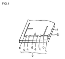
- Fig. 1 is a part of a perspective view of a printed circuit board according to a first embodiment of the present invention.
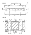
- Fig. 2A is a part of an enlarged top view of a typical wiring pattern formed on the front surface of the printed circuit board according to the embodiment of the present invention.
- Fig. 2B is a part of an enlarged view of a cross section taken on line X-X' shown in Fig. 2A.
- Fig. 3A is a part of an enlarged top view of a typical wiring pattern formed on the front surface of a printed circuit board according to another embodiment of the present invention.
- Fig. 3B is a part of an enlarged view of a cross section taken on line X-X' shown in Fig. 3A.
- FIG. 1 is a perspective view showing a part of a printed circuit board.
- Figs. 2A and 2B are enlarged views of part A of the wiring pattern shown in Fig. 1.
- the printed circuit board includes an insulating board 1 which has been used conventionally, a front wiring pattern 2, and a rear wiring pattern 3.
- the front wiring pattern 2 includes lands 4 for mounting components, terminals 5, and leads 6 for connecting lands 4 and terminals 5 to each other.
- the front wiring pattern 2 comprises a front copper-foil pattern 7 which is formed by etching copper foil provided on the front surface of the insulating board 1, and a plated layer 8A with which the front copper-foil pattern 7 is laminated at the front surface.
- the rear wiring pattern 3 is formed at the rear surface of the insulating board 1, which is opposite the front wiring pattern 2, in a shape which is substantially plane-symmetrical to the front wiring pattern 2. Like the front wiring pattern 2, the rear wiring pattern 3 is formed by a rear copper-foil pattern 9 and a plated layer 8B.
- the insulating board 1 is provided with a plurality of openings 10 which penetrate the front wiring pattern 2 and the rear wiring pattern 3 and are spaced along the longitudinal direction of the front wiring pattern 2.
- the openings 10 may have any shape, such as a circle, an ellipse, a quadrilateral, or a triangle.
- electrically conductive layers such as plated layers 8C, are provided at the inner walls of the openings 10.
- the front wiring pattern 2 and the rear wiring pattern 3 are electrically connected to each other through the plated layers 8C.
- the openings 10 are formed by using a laser beam, by cutting physically, or by punching with the use of a metal die. It is preferred that the maximum dimension of an opening be several millimeters.
- the openings 10 are filled, for example, with solder 11 to form column-shaped electrically conductive fillings.
- the solder 11 is put in the openings 10, for example, by dipping the rear wiring pattern 3 of the printed circuit board in a molten-solder bath.
- a solder resist layer (not shown) is provided in advance.
- the plated layers 8C at the inner walls of the openings 10 become wet with the molten solder 11, and the molten solder 11 goes upward into the openings 10 by capillary action.
- the printed circuit board is cooled down.
- the molten solder 11 becomes hard and the openings 10 are filled with the solder 11. Therefore, the solder 11 does not stick to the surface of the rear wiring pattern 3 and the printed circuit board can be made thin.
- the front wiring pattern 2 and the rear wiring pattern 3 are positively connected by the solder 11 electrically, and the current capacity of the wiring patterns made up of the front wiring pattern 2 and the rear wiring pattern 3 is reliably increased. Therefore, the copper loss of the wiring patterns is reduced.
- the heat capacity of the wiring patterns becomes larger due to the solder 11 with which the openings 10 are filled.
- the solder 11 serves as a heat sink.
- the front wiring pattern 2 is prevented from generating heat.
- the current capacity of the entire area of the front wiring pattern 2 is made larger.
- only a part of the front wiring pattern 2 is provided with openings 10 and conductive fillings 11, whereby the current capacity is only partially increased. Even in this case, since heat generated by a part of the front wiring pattern 2 is reduced, the amount of heat generated by the whole printed circuit board is also reduced.
- the rear wiring pattern 3 is formed in a plane-symmetrical manner to the front wiring pattern 2, and they are positively connected by the solder 11.
- the printed circuit board may alternatively be configured such that the rear wiring pattern 3 is formed plane-symmetrically to only a selected part of the front wiring pattern 2, where a large current flows, and this part of the front wiring pattern 2 is positively connected to the rear wiring pattern 3 by the electrically conductive fillings. In this case, heat generated by the part of the front wiring pattern 2, where a large current flows, is reduced.
- the solder 11 may be allowed to stick to the rear wiring pattern 3 by not providing the solder resist layer. In that case, the current capacity of the wiring patterns becomes even larger.
- a plurality of printed circuit boards which are formed in this way may be stacked to form a multilayer printed circuit board.
- An insulating board 1 is provided with a plurality of long and narrow openings 10 which have a width of several millimeters or less and which extend in the longitudinal direction through a front wiring pattern 2 and a rear wiring pattern 3.
- the openings 10 are formed by using a laser beam, by cutting physically, or by punching with the use of a metal die.
- the openings 10 are also provided with electrically conductive layers, such as plated layers 8C, at the inner walls.
- the openings 10 are filled with solder 11 to form electrically conductive fillings.
- the current capacity of the wiring patterns in the printed circuit board becomes larger, and the electrically conductive fillings serve as current paths to reduce the copper loss of the wiring patterns.
- the solder 11 with which the openings 10 are filled has a larger volume than the electrically conductive fillings shown in Figs. 2A and 2B, and it works more effectively as a heat sink. As a result, the front wiring pattern 2 is prevented from generating heat.
Landscapes
- Engineering & Computer Science (AREA)
- Microelectronics & Electronic Packaging (AREA)
- Manufacturing & Machinery (AREA)
- Structure Of Printed Boards (AREA)
- Combinations Of Printed Boards (AREA)
- Printing Elements For Providing Electric Connections Between Printed Circuits (AREA)
Applications Claiming Priority (3)
| Application Number | Priority Date | Filing Date | Title |
|---|---|---|---|
| JP7265440A JPH09107162A (ja) | 1995-10-13 | 1995-10-13 | プリント回路基板 |
| JP265440/95 | 1995-10-13 | ||
| JP26544095 | 1995-10-13 |
Publications (3)
| Publication Number | Publication Date |
|---|---|
| EP0768813A2 true EP0768813A2 (fr) | 1997-04-16 |
| EP0768813A3 EP0768813A3 (fr) | 1998-05-13 |
| EP0768813B1 EP0768813B1 (fr) | 2004-01-02 |
Family
ID=17417188
Family Applications (1)
| Application Number | Title | Priority Date | Filing Date |
|---|---|---|---|
| EP96402167A Expired - Lifetime EP0768813B1 (fr) | 1995-10-13 | 1996-10-11 | Panneaux à circuit imprimé |
Country Status (6)
| Country | Link |
|---|---|
| US (1) | US5958562A (fr) |
| EP (1) | EP0768813B1 (fr) |
| JP (1) | JPH09107162A (fr) |
| KR (1) | KR100315827B1 (fr) |
| DE (1) | DE69631236D1 (fr) |
| TW (1) | TW452317U (fr) |
Cited By (3)
| Publication number | Priority date | Publication date | Assignee | Title |
|---|---|---|---|---|
| WO2006067689A3 (fr) * | 2004-12-21 | 2006-09-21 | Koninkl Philips Electronics Nv | Systeme de carte imprimee |
| EP2618641A1 (fr) * | 2012-01-11 | 2013-07-24 | E.G.O. ELEKTRO-GERÄTEBAU GmbH | Porte-composant, conducteur électrique et procédé de fabrication d'un porte-composant ainsi que conducteur électrique |
| EP2699065A4 (fr) * | 2012-06-18 | 2014-08-13 | Sanyo Electric Co | Substrat de circuit |
Families Citing this family (17)
| Publication number | Priority date | Publication date | Assignee | Title |
|---|---|---|---|---|
| US6598291B2 (en) | 1998-03-20 | 2003-07-29 | Viasystems, Inc. | Via connector and method of making same |
| US6303881B1 (en) * | 1998-03-20 | 2001-10-16 | Viasystems, Inc. | Via connector and method of making same |
| US6713685B1 (en) * | 1998-09-10 | 2004-03-30 | Viasystems Group, Inc. | Non-circular micro-via |
| JP2006011239A (ja) * | 2004-06-29 | 2006-01-12 | Kyocera Corp | 液晶表示装置 |
| KR20060045208A (ko) * | 2004-11-12 | 2006-05-17 | 삼성테크윈 주식회사 | 반도체 팩키지용 회로기판 및 이의 제조방법 |
| JP4654942B2 (ja) * | 2006-02-28 | 2011-03-23 | ミネベア株式会社 | 面状照明装置 |
| US7545461B2 (en) | 2006-07-25 | 2009-06-09 | Kyocera Corporation | Liquid crystal display device |
| US7561430B2 (en) * | 2007-04-30 | 2009-07-14 | Watlow Electric Manufacturing Company | Heat management system for a power switching device |
| JP2009206324A (ja) * | 2008-02-28 | 2009-09-10 | Fuji Electric Systems Co Ltd | 多層プリント配線基板 |
| JP2010067668A (ja) * | 2008-09-09 | 2010-03-25 | Nippon Avionics Co Ltd | プリント配線板 |
| KR100968977B1 (ko) * | 2008-10-17 | 2010-07-14 | 삼성전기주식회사 | 무수축 세라믹 기판 및 무수축 세라믹 기판의 제조 방법 |
| IT1400040B1 (it) * | 2010-05-27 | 2013-05-17 | Elenos S R L | Dispositivo lc per apparecchiature di potenza in radiofrequenza |
| JP2015128107A (ja) * | 2013-12-27 | 2015-07-09 | 三菱重工業株式会社 | 回路基板及び回路基板形成装置並びに回路基板形成方法 |
| KR102262908B1 (ko) * | 2014-11-19 | 2021-06-09 | 삼성전기주식회사 | 다층 인쇄회로기판 및 그 제조 방법 |
| JP6468571B2 (ja) * | 2017-02-07 | 2019-02-13 | 株式会社三共 | 遊技機 |
| KR102302499B1 (ko) | 2020-12-03 | 2021-09-16 | 주식회사 기가레인 | 전원 전송 라인을 포함하는 연성회로기판 |
| KR102366495B1 (ko) * | 2021-05-03 | 2022-02-23 | 주식회사 기가레인 | 전원 전송 라인을 포함하는 연성회로기판 |
Family Cites Families (12)
| Publication number | Priority date | Publication date | Assignee | Title |
|---|---|---|---|---|
| GB982405A (en) * | 1961-06-29 | 1965-02-03 | Int Resistance Co | Improvements in or relating to printed circuit panels |
| US3330695A (en) * | 1962-05-21 | 1967-07-11 | First Safe Deposit Nat Bank Of | Method of manufacturing electric circuit structures |
| US3568312A (en) * | 1968-10-04 | 1971-03-09 | Hewlett Packard Co | Method of making printed circuit boards |
| US3708876A (en) * | 1969-01-28 | 1973-01-09 | Burroughs Corp | Vacuum-heat treatment of printed circuit boards |
| US4826720A (en) * | 1985-11-07 | 1989-05-02 | General Electric Company | Directly solderable three-dimensional electrically conductive circuit components and process for the preparation thereof |
| JPH0754874B2 (ja) * | 1986-10-20 | 1995-06-07 | フアナツク株式会社 | 多層プリント配線板 |
| EP0516866A1 (fr) * | 1991-05-03 | 1992-12-09 | International Business Machines Corporation | Structure modulaire d'interconnexion multicouche |
| JP3218542B2 (ja) * | 1991-07-02 | 2001-10-15 | ジャパンゴアテックス株式会社 | 電子回路基板及び半導体チップキャリヤー用シート |
| US5288541A (en) * | 1991-10-17 | 1994-02-22 | International Business Machines Corporation | Method for metallizing through holes in thin film substrates, and resulting devices |
| JPH06204628A (ja) * | 1992-12-10 | 1994-07-22 | Hitachi Aic Inc | プリント配線板 |
| JPH06326436A (ja) * | 1993-05-14 | 1994-11-25 | Sony Corp | プリント配線基板 |
| US5408053A (en) * | 1993-11-30 | 1995-04-18 | Hughes Aircraft Company | Layered planar transmission lines |
-
1995
- 1995-10-13 JP JP7265440A patent/JPH09107162A/ja active Pending
-
1996
- 1996-10-07 TW TW089219064U patent/TW452317U/zh not_active IP Right Cessation
- 1996-10-07 US US08/726,747 patent/US5958562A/en not_active Expired - Fee Related
- 1996-10-11 DE DE69631236T patent/DE69631236D1/de not_active Expired - Lifetime
- 1996-10-11 EP EP96402167A patent/EP0768813B1/fr not_active Expired - Lifetime
- 1996-10-11 KR KR1019960045336A patent/KR100315827B1/ko not_active Expired - Fee Related
Cited By (3)
| Publication number | Priority date | Publication date | Assignee | Title |
|---|---|---|---|---|
| WO2006067689A3 (fr) * | 2004-12-21 | 2006-09-21 | Koninkl Philips Electronics Nv | Systeme de carte imprimee |
| EP2618641A1 (fr) * | 2012-01-11 | 2013-07-24 | E.G.O. ELEKTRO-GERÄTEBAU GmbH | Porte-composant, conducteur électrique et procédé de fabrication d'un porte-composant ainsi que conducteur électrique |
| EP2699065A4 (fr) * | 2012-06-18 | 2014-08-13 | Sanyo Electric Co | Substrat de circuit |
Also Published As
| Publication number | Publication date |
|---|---|
| EP0768813B1 (fr) | 2004-01-02 |
| DE69631236D1 (de) | 2004-02-05 |
| US5958562A (en) | 1999-09-28 |
| EP0768813A3 (fr) | 1998-05-13 |
| KR100315827B1 (ko) | 2002-01-17 |
| KR970025297A (ko) | 1997-05-30 |
| TW452317U (en) | 2001-08-21 |
| JPH09107162A (ja) | 1997-04-22 |
Similar Documents
| Publication | Publication Date | Title |
|---|---|---|
| EP0768813A2 (fr) | Panneaux à circuit imprimé | |
| EP0920055B1 (fr) | Dispositif de refroidissement pour un composant générant de la chaleur sur un circuit imprimé | |
| CA1312146C (fr) | Cartes de circuit imprime a segment concu pour recevoir des broches | |
| US4413309A (en) | Printed circuit board | |
| US6515222B2 (en) | Printed circuit board arrangement | |
| EP0568313A2 (fr) | Procédé de production d'une plaque à circuit imprimé multicouche | |
| EP0430157A2 (fr) | Panneau de circuit composé et son procédé de fabrication | |
| US7381905B2 (en) | Structure for fixing an electronic device to a substrate | |
| US5619018A (en) | Low weight multilayer printed circuit board | |
| EP0159771B1 (fr) | Résistances-chip et procédé de leur fabrication | |
| EP1610596B1 (fr) | Gestion de la chaleur dans un ensemble de cartes à circuits | |
| US5763060A (en) | Printed wiring board | |
| JPH0747897Y2 (ja) | プリント基板 | |
| JP2521034B2 (ja) | プリント配線基板 | |
| JP2926902B2 (ja) | プリント配線基板 | |
| JPH0846338A (ja) | 配線板 | |
| JP3928152B2 (ja) | プリント配線板 | |
| EP1385363B1 (fr) | Carte de circuits imprimes et procede permettant sa realisation, et carte de circuits imprimes laminee | |
| JPH06204628A (ja) | プリント配線板 | |
| JP4838034B2 (ja) | プリント配線基板およびその製造方法 | |
| JPS5998584A (ja) | 印刷配線板 | |
| JPH1051094A (ja) | プリント配線板及びその製造方法 | |
| EP0568311A2 (fr) | Procédé de production d'une plaque à circuit imprimé multicouche | |
| JPH0214207Y2 (fr) | ||
| JPS6286894A (ja) | 印刷配線基板 |
Legal Events
| Date | Code | Title | Description |
|---|---|---|---|
| PUAI | Public reference made under article 153(3) epc to a published international application that has entered the european phase |
Free format text: ORIGINAL CODE: 0009012 |
|
| AK | Designated contracting states |
Kind code of ref document: A2 Designated state(s): DE FR GB |
|
| PUAL | Search report despatched |
Free format text: ORIGINAL CODE: 0009013 |
|
| AK | Designated contracting states |
Kind code of ref document: A3 Designated state(s): DE FR GB |
|
| 17P | Request for examination filed |
Effective date: 19981104 |
|
| 17Q | First examination report despatched |
Effective date: 20020730 |
|
| GRAH | Despatch of communication of intention to grant a patent |
Free format text: ORIGINAL CODE: EPIDOS IGRA |
|
| GRAH | Despatch of communication of intention to grant a patent |
Free format text: ORIGINAL CODE: EPIDOS IGRA |
|
| GRAS | Grant fee paid |
Free format text: ORIGINAL CODE: EPIDOSNIGR3 |
|
| GRAA | (expected) grant |
Free format text: ORIGINAL CODE: 0009210 |
|
| AK | Designated contracting states |
Kind code of ref document: B1 Designated state(s): DE FR GB |
|
| PG25 | Lapsed in a contracting state [announced via postgrant information from national office to epo] |
Ref country code: FR Free format text: LAPSE BECAUSE OF FAILURE TO SUBMIT A TRANSLATION OF THE DESCRIPTION OR TO PAY THE FEE WITHIN THE PRESCRIBED TIME-LIMIT Effective date: 20040102 |
|
| REG | Reference to a national code |
Ref country code: GB Ref legal event code: FG4D |
|
| REF | Corresponds to: |
Ref document number: 69631236 Country of ref document: DE Date of ref document: 20040205 Kind code of ref document: P |
|
| PG25 | Lapsed in a contracting state [announced via postgrant information from national office to epo] |
Ref country code: DE Free format text: LAPSE BECAUSE OF FAILURE TO SUBMIT A TRANSLATION OF THE DESCRIPTION OR TO PAY THE FEE WITHIN THE PRESCRIBED TIME-LIMIT Effective date: 20040403 |
|
| PLBE | No opposition filed within time limit |
Free format text: ORIGINAL CODE: 0009261 |
|
| STAA | Information on the status of an ep patent application or granted ep patent |
Free format text: STATUS: NO OPPOSITION FILED WITHIN TIME LIMIT |
|
| 26N | No opposition filed |
Effective date: 20041005 |
|
| EN | Fr: translation not filed | ||
| PGFP | Annual fee paid to national office [announced via postgrant information from national office to epo] |
Ref country code: GB Payment date: 20071010 Year of fee payment: 12 |
|
| GBPC | Gb: european patent ceased through non-payment of renewal fee |
Effective date: 20081011 |
|
| PG25 | Lapsed in a contracting state [announced via postgrant information from national office to epo] |
Ref country code: GB Free format text: LAPSE BECAUSE OF NON-PAYMENT OF DUE FEES Effective date: 20081011 |