EP0769743A2 - Dispositif de mémoire à semi-conducteur avec puce de petite taille et temps d'accès de redondance réduit - Google Patents
Dispositif de mémoire à semi-conducteur avec puce de petite taille et temps d'accès de redondance réduit Download PDFInfo
- Publication number
- EP0769743A2 EP0769743A2 EP96116710A EP96116710A EP0769743A2 EP 0769743 A2 EP0769743 A2 EP 0769743A2 EP 96116710 A EP96116710 A EP 96116710A EP 96116710 A EP96116710 A EP 96116710A EP 0769743 A2 EP0769743 A2 EP 0769743A2
- Authority
- EP
- European Patent Office
- Prior art keywords
- redundancy
- word
- normal
- line
- memory cell
- Prior art date
- Legal status (The legal status is an assumption and is not a legal conclusion. Google has not performed a legal analysis and makes no representation as to the accuracy of the status listed.)
- Granted
Links
Images



Classifications
-
- H—ELECTRICITY
- H10—SEMICONDUCTOR DEVICES; ELECTRIC SOLID-STATE DEVICES NOT OTHERWISE PROVIDED FOR
- H10B—ELECTRONIC MEMORY DEVICES
- H10B12/00—Dynamic random access memory [DRAM] devices
- H10B12/50—Peripheral circuit region structures
-
- G—PHYSICS
- G11—INFORMATION STORAGE
- G11C—STATIC STORES
- G11C29/00—Checking stores for correct operation ; Subsequent repair; Testing stores during standby or offline operation
- G11C29/70—Masking faults in memories by using spares or by reconfiguring
- G11C29/78—Masking faults in memories by using spares or by reconfiguring using programmable devices
- G11C29/80—Masking faults in memories by using spares or by reconfiguring using programmable devices with improved layout
-
- G—PHYSICS
- G11—INFORMATION STORAGE
- G11C—STATIC STORES
- G11C29/00—Checking stores for correct operation ; Subsequent repair; Testing stores during standby or offline operation
- G11C29/70—Masking faults in memories by using spares or by reconfiguring
- G11C29/78—Masking faults in memories by using spares or by reconfiguring using programmable devices
- G11C29/84—Masking faults in memories by using spares or by reconfiguring using programmable devices with improved access time or stability
Definitions
- the present invention relates to a semiconductor memory device, and more particularly to a semiconductor memory device equipped with a redundancy circuit which compensates for a defect in the memory cell arrays.
- redundancy circuit is indispensable for removing the effect of such defects. Redundancy circuits will now be briefly explained. Finished semiconductor memories undergo a proving inspection to determine whether the memory cells have a defect. When the result of the inspection indicates the presence of a defect in the memory cells, an alternative memory cell is provided which operates instead of the defective region.
- the alternative memory cell is a redundancy circuit; that is, a redundancy circuit is a backup memory cell which takes the place of the defective portion of main memory cells (hereunder referred to as redundancy cell).
- Fig. 8 is an illustration of circuitry of a conventional memory equipped with a redundancy circuit.
- the illustrated circuitry comprises a plurality of normal cell arrays 21 and 23, and sense amplifiers 11 - 14 placed above and under the respective normal cell arrays 21 and 23.
- a redundancy cell array 33 is provided for the normal cell arrays 21 and 23, and sense amplifiers 10 and 11 are used as the sense amplifiers for the redundancy cell array 33.
- sense amplifier controllers 40 - 44 are provided for the respective sense amplifiers, while normal decoder & word drivers 60 and 61 are provided for the normal cell arrays 21 and 23, and a redundancy word driver 53 is provided for the redundancy cell array 33.
- a normal address predecoder & driver 90 produces sense amplifier-selecting signals SAMPSELECT 0-m, and concurrently produces a decoder-selecting signal DECSELECT which determines the normal decoder & word driver to be selected.
- SAMPSELECT the address which corresponds to the normal cell array 23
- DECSELECT the normal decoder & word driver
- a redundancy judgment circuit 70 produces a redundancy judgment signal RDN which indicates selection of a defective address to control the activation/inactivation of the respective sense amplifier controllers.
- one of the signals RED0 - REDn output from the redundancy fuse circuits 89 is turned to a high level, corresponding to the defective address, and one of the redundancy word drivers 53 is selected in response to the high level of the signal RED to select a redundancy word line.
- the signals RED0 - REDn are concurrently input to the redundancy judgment circuit 70 to turn the signal RDN to a high level as well.
- the signal RDN is input to all the sense amplifier controllers 40 - 44 and turns off all the sense amplifier controllers 42 - 44 for the normal cell arrays. Also, the sense amplifier controllers 40 and 41 which corresponds to the redundancy cell array 33 are turned on by the signal RDN.
- Fig. 9 is a circuit diagram illustrative of the redundancy fuse circuit 89 and the redundancy judgment circuit 70 in Fig. 8.
- the redundancy fuse circuits are provided in number "n" (89-0 through 89-n) corresponding to the "n" normal cell arrays.
- the output signals RED0 - REDn from the redundancy fuse circuits 89 are input to the respective gates of transistors 130 - 134 in the redundancy judgment circuit 70, with the drains of the transistors wired-NOR-connected.
- the wired-NOR-connecting line is pulled up and connected to a power supply Vcc by a transistor 140, and its potential is derived as an output signal, or the redundancy judgment signal RDN via an inverter 125.
- a precharge signal RST which is input to the gate of the transistor 140 is active, and all the input signals RED0 - REDn are at low levels at the initial state. Accordingly, the wired-NOR-connecting line is precharged to a high level.
- the precharge signal RST is then inactivated when the process proceeds to the activation stage, whereas the transistor 140 is turned off, with the wired-NOR-connecting line held in a high floating state.
- the redundancy judgment signal RDN changes from a low level to a high level.
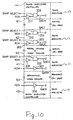
- Fig. 10 is an illustration of part of the sense amplifier controller circuit.
- Signals SAMPSELECT 0-m and signals RDN are input to sense amplifier controllers 40 - 44.
- the sense amplifiers are inactivated when the outputs of the sense amplifier controllers are at high levels, and are activated when at low levels.
- the sense amplifiers are selected when the signals SAMPSELECT are at high levels.
- the sense amplifiers 11 - 14 must be activated when the access address is not a defective address.
- the signals RDN since the signals RDN become low, NAND gates 202 - 205 pass sense amplifier-selecting signals to activate the selected sense amplifiers.
- the signals SAMPSELECT 0-m become invalid to thereby inactivate the sense amplifiers.
- sense amplifier-activating signals SAER for the redundancy cell arrays are output at low levels to activate the sense amplifiers 10 and 11 which correspond to the redundancy cell array 33.
- the sense amplifiers 11 - 13 operate as the sense amplifiers for the corresponding cell arrays located above and under them, when a plurality of sense amplifier-activating signals SAE are input as the sense amplifier 12 illustrated in Fig. 10, the low-level signal SAE takes precedence, in other words, the sense amplifier is activated.
- the redundancy cell arrays are prepared to compensate for defects, it becomes impossible to perform replacement when the arrays fail. From a process viewpoint, however, the cell arrays and memory cells near the sense amplifiers have higher probabilities of failure, since defects may be caused at the ends of the cell arrays due to steps, etc.
- the present invention minimizes delays due to wiring between the blocks, and minimizes the wiring area by placing the redundancy fuse circuits, or the redundancy control circuit and the redundancy word drivers at locations to produce the shortest wiring lengths between them (preferably so as to achieve linear wiring between the circuits).
- the sense amplifiers may be designed so as to be used for both the normal cell arrays and the redundancy cell arrays. Therefore, there is no need to provide sense amplifiers used solely for the redundancy cell arrays, and this decreases the chip area.
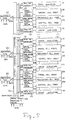
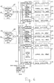
- Fig. 1 is a block diagram illustrative of an embodiment according to the present invention.
- Redundancy cell arrays 30-32 are provided corresponding to normal cell arrays 20-23, and the respective redundancy cell arrays are placed in the corresponding normal cell arrays in a mixed manner to allow the sense amplifiers for the normal cell arrays to be used also as those for the redundancy cell arrays.
- redundancy word drivers 50-53 are provided corresponding to the redundancy cell arrays 30-32 respectively.
- redundancy fuse circuits 80-82 and a redundancy judgment circuit 70 for detecting a defective address are placed so as to minimize the wiring lengths from the respective redundancy word drivers and the respective amplifier controllers, that is, so as to achieve linear wiring.
- the redundancy word driver, the redundancy fuse circuit and the redundancy cell array are arranged in line.
- the cell array which may replace each normal cell array, matches only one word line.
- a normal address predecoder & driver 90 produces sense amplifier-selecting signals SAMPSELECT 0-n and a decoder-selecting signal DECSELECT likewise as in the prior art.
- the redundancy fuse circuits 81-82 corresponding to the normal cell arrays detect whether the input access address ADR is a defective address.
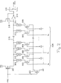
- Fig. 2 is an illustration of the redundancy fuse circuits.
- the address signals ADR and their complementary signals (A0 - An and their inverted signals) are input to the respective gates of NMOS transistors 303-308, with the respective drains of the respective transistors 303-308 commonly connected to a wired-NOR line 315 via fuses 309-314, respectively.
- the sources of the NMOS transistors 303-308 are grounded via a transistor 302.
- the wired-NOR line 315 is designed to be precharged to a high level by a PMOS transistor 301, and the output from the wired-NOR line 315 is derived as a redundancy fuse output signal RED, or the redundancy control information via an inverter 316 and a latch circuit 319.
- the PMOS transistor 318 is used to maintain the wired-NOR line 315 at a high level.
- the precharge signal PRC becomes low, while the transistor 301 is turned on, to precharge the wired-NOR line 315 to a high level.
- the NMOS transistor 302 is in the off state.
- the signal PRC becomes high, the PMOS transistor 301 is turned off. Accordingly, the wired-NOR line 315 is brought to the high-level floating state, and becomes normal state when the NMOR transistor 302 is concurrently turned on.
- the wired-NOR line 315 When the addresses ADR are input in the normal state, the wired-NOR line 315 is brought to a low level by the NMOS transistors 303-308. However, when the associated fuse circuit detects a defective address, the wired-NOR line 315 is kept in the high-level floating state. This is achieved by appropriately selecting and burning the fuses 309-314.
- the addresses ADR are addresses corresponding to word lines. Although addresses may be decoded by a variety of methods, here, assuming that the addresses A0 - An have a one-to-one correspondence with the word lines for simplicity. Then, an explanation will be given regarding the case where the memory cells of the word line which corresponds to the address A1 cause a defective address.
- the access addresses ADR which correspond to the address A1 are 0, 1 and 0, corresponding to A0, A1 and An, respectively, in the drawing.
- the fuses 310, 311 and 314 are burnt.
- low-level signals are input to the gates of the NMOS transistors 303, 306 and 307, and thus these transistors are brought out of conduction.
- high-level signals are input to the gates of the NMOS transistors 304, 305 and 308, nevertheless, since the fuses 310, 311 and 314 have been burnt, these transistors are out of conduction as well, thus maintaining the high floating state of the wired-NOR line 315.
- a redundancy judgment circuit 70 produces a redundancy judgment signal RDN which indicates selection of a defective address when the signals RED0 - REDn are input, to control the activation/inactivation of the respective sense amplifier controllers 40-44.
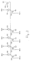
- Fig. 3 is an illustration of the redundancy judgment circuit 70.
- inverters 120-124 are provided corresponding to the sense amplifier controllers. The rest of the configuration is the same as that shown in Fig. 9.
- the transistor 140 is on due to a precharge signal RST, while the transistors 130-134 are off, and therefore the wired-NOR line is in a high-level floating state.
- the signal RST is first inactivated, and the wired-NOR line is kept in a high-level floating state.
- one of the redundancy outputs RED0 - REDn becomes high corresponding to the defective address, one of the transistors 130-134 is turned on, the wired-NOR line is rapidly brought to a low level, and all the signals RDN are output at high levels by the inverters 120-124.
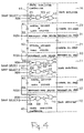
- Fig. 4 is an illustration of part of the sense amplifier controller circuit.
- the signals RED 0-n and RDN are at low levels during normal access, a sense amplifier controller selected in response to the signal SAMPSELECT operates.
- the signal RED1 is produced as high level
- the outputs of NAND gates 100-103 are fixed to high levels due to the high level of the signal RDN.
- inverters 212-215 either inputs to NOR gates 110-113 are at low levels. Therefore, the outputs of the NOR gates 110-113 become high to inactivate and suspend the sense amplifiers.
- the NOR gate 112 to which the signal RED1 is input produces a high-level output to activate the sense amplifier 11 for operating the corresponding redundancy cell array 30.
- the signal RED and the signal RDN are input at almost the same time.
- FIG. 5 A second embodiment which is designed to overcome the drawback which the fail of the redundancy cell arrays is shown in Fig. 5, in which like portions are designated by like character references used in Fig. 1.
- the normal cell array 21 shown in Fig. 1 is divided into two upper and lower portions (21A, 21B) roughly in the center portion, along the direction of the word line, and a redundancy cell array 30 is placed in the center portion. That is, it is designed so that the redundancy ceyl array is prevented from failure by being placed in the center portion of the normal cell array instead of being placed at one end of the normal cell array. This configuration applies to the other normal cell arrays.
- FIG. 6 A third embodiment is shown in Fig. 6, in which like portions are designated by like character references used in Fig. 1. Redundancy cell arrays are provided for all the normal cell arrays with a one-to-one correspondence according to the first and second embodiments shown in Fig. 1 and Fig. 5, whereas redundancy cell arrays are not provided for all the normal cell arrays according to the third embodiment. The reason will now be explained.
- the placement according to the third embodiment is for placement of a minimum number of redundancy cell arrays.
- the decoder section of the normal decoder & driver 60 is included into a main word decoder and sub word decoder to allow selection of eight sub word lines per one main word line.
- a split decoding is used here.
- the minimum number of redundancy cell arrays per normal cell array may be less than eight.
- the minimum number of redundancy cell arrays corresponds to four word lines, this assumption applies to the first, second and third embodiments. Therefore, according to the first and the second embodiments as shown Fig.
- a redundancy main word line 722 is replaced by eight redundancy sub word lines 724, which is same replacement number with the normal main word line. Therefore, a redundancy sub word decoder 717 requires eight word driver lines 720 in common to a normal sub word driver 716.
- a word line controller 718 decodes a sub word address for the sub word decoders which corresponds to an address signals.
- a second effect is a decrease in the chip area, since, as described above, the redundancy fuse circuits and the redundancy word drivers are placed with the shortest wiring lengths between them, and also the redundancy judgment circuit is placed in parallel with the two circuits, sandwiched between them, to minimize the increase in the wiring area. More specifically, since usually the wiring widths and the wiring distances required are both on the order of 1 ⁇ m, two wires extend with an approximately 4 ⁇ m width. For example, a 256 Mbit DRAM, which needs 32 redundancy output signals RED, needs a width on the order of 64 ⁇ m. According to the present invention, since the entire redundancy judgment circuit fits into the width (the maximum size of the gate is estimated to be approximately 10 ⁇ m), the chip area is greatly reduced.
- a fourth effect is a reduction in the chip area, since the redundancy memory cell arrays are not provided for all the memory cell array plates, and the word line control circuits may be likewise configured, with the normal word drivers and the redundancy word drivers.
Landscapes
- For Increasing The Reliability Of Semiconductor Memories (AREA)
- Dram (AREA)
- Semiconductor Memories (AREA)
- Design And Manufacture Of Integrated Circuits (AREA)
- Techniques For Improving Reliability Of Storages (AREA)
Applications Claiming Priority (3)
| Application Number | Priority Date | Filing Date | Title |
|---|---|---|---|
| JP26891495 | 1995-10-18 | ||
| JP268914/95 | 1995-10-18 | ||
| JP7268914A JP3036411B2 (ja) | 1995-10-18 | 1995-10-18 | 半導体記憶集積回路装置 |
Publications (3)
| Publication Number | Publication Date |
|---|---|
| EP0769743A2 true EP0769743A2 (fr) | 1997-04-23 |
| EP0769743A3 EP0769743A3 (fr) | 1999-07-28 |
| EP0769743B1 EP0769743B1 (fr) | 2003-01-02 |
Family
ID=17465034
Family Applications (1)
| Application Number | Title | Priority Date | Filing Date |
|---|---|---|---|
| EP96116710A Expired - Lifetime EP0769743B1 (fr) | 1995-10-18 | 1996-10-17 | Dispositif de mémoire à semi-conducteur avec puce de petite taille et temps d'accès de redondance réduit |
Country Status (7)
| Country | Link |
|---|---|
| US (1) | US5841708A (fr) |
| EP (1) | EP0769743B1 (fr) |
| JP (1) | JP3036411B2 (fr) |
| KR (1) | KR100195677B1 (fr) |
| CA (1) | CA2188101C (fr) |
| DE (1) | DE69625571T2 (fr) |
| TW (1) | TW317634B (fr) |
Cited By (1)
| Publication number | Priority date | Publication date | Assignee | Title |
|---|---|---|---|---|
| CN102024816A (zh) * | 2009-09-14 | 2011-04-20 | 瑞萨电子株式会社 | 半导体存储器件 |
Families Citing this family (17)
| Publication number | Priority date | Publication date | Assignee | Title |
|---|---|---|---|---|
| KR100486217B1 (ko) * | 1997-11-06 | 2005-09-08 | 삼성전자주식회사 | 메모리셀제어회로를구비하는반도체메모리장치 |
| JPH11154398A (ja) * | 1997-11-20 | 1999-06-08 | Oki Electric Ind Co Ltd | 半導体記憶装置 |
| JP2000100195A (ja) * | 1998-09-22 | 2000-04-07 | Nec Corp | 冗長回路を有する半導体記憶装置 |
| JP2000348496A (ja) * | 1999-06-09 | 2000-12-15 | Nec Corp | 半導体記憶装置 |
| JP2001101892A (ja) * | 1999-09-30 | 2001-04-13 | Mitsubishi Electric Corp | 半導体記憶装置 |
| US6166974A (en) * | 1999-10-28 | 2000-12-26 | Vanguard International Semiconductor Corp. | Dynamic precharge redundant circuit for semiconductor memory device |
| US6256237B1 (en) * | 1999-12-28 | 2001-07-03 | United Microelectronics Corp. | Semiconductor device and method for repairing failed memory cell by directly programming fuse memory cell |
| JP2001273788A (ja) * | 2000-03-29 | 2001-10-05 | Hitachi Ltd | 半導体記憶装置 |
| JP2002063797A (ja) * | 2000-08-22 | 2002-02-28 | Mitsubishi Electric Corp | 不揮発性半導体記憶装置 |
| JP2003100094A (ja) * | 2001-09-27 | 2003-04-04 | Mitsubishi Electric Corp | 半導体記憶装置 |
| JP2008097675A (ja) * | 2006-10-06 | 2008-04-24 | Elpida Memory Inc | 半導体装置 |
| KR100851856B1 (ko) | 2006-12-11 | 2008-08-13 | 삼성전자주식회사 | 반도체 메모리 장치 및 그 리페어 방법 |
| JP5494455B2 (ja) * | 2010-12-09 | 2014-05-14 | 富士通セミコンダクター株式会社 | 半導体記憶装置 |
| US9030897B2 (en) * | 2012-08-31 | 2015-05-12 | SK Hynix Inc. | Memory and memory system for preventing degradation of data |
| CN113918481A (zh) * | 2017-07-30 | 2022-01-11 | 纽罗布拉德有限公司 | 一种存储器芯片 |
| CN110692047A (zh) * | 2019-05-19 | 2020-01-14 | 深圳齐心集团股份有限公司 | 一种基于大数据的文具信息调度系统 |
| US11289151B2 (en) | 2019-11-08 | 2022-03-29 | Micron Technology, Inc. | Cross-coupled transistor threshold voltage mismatch compensation and related devices, systems, and methods |
Family Cites Families (8)
| Publication number | Priority date | Publication date | Assignee | Title |
|---|---|---|---|---|
| US4406013A (en) * | 1980-10-01 | 1983-09-20 | Intel Corporation | Multiple bit output dynamic random-access memory |
| JPH0666394B2 (ja) * | 1983-12-16 | 1994-08-24 | 富士通株式会社 | 半導体記憶装置 |
| JPS6337899A (ja) * | 1986-07-30 | 1988-02-18 | Mitsubishi Electric Corp | 半導体記憶装置 |
| JPS63220500A (ja) * | 1987-03-09 | 1988-09-13 | Mitsubishi Electric Corp | 半導体記憶装置の冗長回路 |
| JP2782948B2 (ja) * | 1990-11-16 | 1998-08-06 | 日本電気株式会社 | 半導体メモリ |
| KR940008208B1 (ko) * | 1990-12-22 | 1994-09-08 | 삼성전자주식회사 | 반도체 메모리장치의 리던던트 장치 및 방법 |
| EP0499131A1 (fr) * | 1991-02-12 | 1992-08-19 | Texas Instruments Incorporated | Redondance de ligne à haute rendement pour RAM dynamique |
| JP2616544B2 (ja) * | 1993-09-22 | 1997-06-04 | 日本電気株式会社 | 半導体記憶装置 |
-
1995
- 1995-10-18 JP JP7268914A patent/JP3036411B2/ja not_active Expired - Fee Related
-
1996
- 1996-10-17 DE DE69625571T patent/DE69625571T2/de not_active Expired - Fee Related
- 1996-10-17 CA CA002188101A patent/CA2188101C/fr not_active Expired - Fee Related
- 1996-10-17 EP EP96116710A patent/EP0769743B1/fr not_active Expired - Lifetime
- 1996-10-18 US US08/731,742 patent/US5841708A/en not_active Expired - Lifetime
- 1996-10-18 KR KR1019960046890A patent/KR100195677B1/ko not_active Expired - Fee Related
- 1996-10-18 TW TW085112744A patent/TW317634B/zh active
Cited By (2)
| Publication number | Priority date | Publication date | Assignee | Title |
|---|---|---|---|---|
| CN102024816A (zh) * | 2009-09-14 | 2011-04-20 | 瑞萨电子株式会社 | 半导体存储器件 |
| CN102024816B (zh) * | 2009-09-14 | 2015-02-11 | 瑞萨电子株式会社 | 半导体存储器件 |
Also Published As
| Publication number | Publication date |
|---|---|
| KR100195677B1 (ko) | 1999-06-15 |
| EP0769743A3 (fr) | 1999-07-28 |
| KR970024193A (ko) | 1997-05-30 |
| TW317634B (fr) | 1997-10-11 |
| US5841708A (en) | 1998-11-24 |
| CA2188101C (fr) | 2000-12-12 |
| JPH09115297A (ja) | 1997-05-02 |
| DE69625571T2 (de) | 2003-11-27 |
| JP3036411B2 (ja) | 2000-04-24 |
| DE69625571D1 (de) | 2003-02-06 |
| CA2188101A1 (fr) | 1997-04-19 |
| EP0769743B1 (fr) | 2003-01-02 |
Similar Documents
| Publication | Publication Date | Title |
|---|---|---|
| US5841708A (en) | Semiconductor memory device having small chip size and redundancy access time | |
| US5349556A (en) | Row redundancy circuit sharing a fuse box | |
| US7106643B2 (en) | Method for manufacturing memory device provided with a defect recovery mechanism featuring a redundancy circuit | |
| KR0172393B1 (ko) | 탄력적인 컬럼구제 기능을 가지는 반도체 메모리 장치 | |
| KR0167678B1 (ko) | 컬럼 리던던시 회로를 가지는 반도체 메모리 장치 | |
| EP0472209B1 (fr) | Dispositif de mémoire à semi-conducteur ayant un circuit de redondance | |
| KR20000067346A (ko) | 리던던트 로우 대체 구조를 가지는 반도체 메모리 장치 및 그것의 로우 구동 방법 | |
| GB2302748A (en) | Semiconductor memory cell repair | |
| EP0562548B1 (fr) | Dispositif de mémoire à semi-conducteur à redondance | |
| KR100207512B1 (ko) | 동기형 반도체 메모리 장치의 다이내믹 컬럼 리던던시 구동 회로 | |
| KR100307567B1 (ko) | 용장회로를구비한반도체기억장치 | |
| KR100322538B1 (ko) | 래치 셀을 채용하는 리던던시 회로 | |
| JP3642905B2 (ja) | メモリセルアレイブロックの再編成が可能な半導体メモリ装置 | |
| US6366509B2 (en) | Method and apparatus for repairing defective columns of memory cells | |
| KR100320683B1 (ko) | 스탠바이 전류불량 구제기능을 가지는 반도체 메모리 장치 | |
| JP3673637B2 (ja) | 冗長回路を備えた半導体メモリ装置 | |
| US6335892B1 (en) | Method to electrically program antifuses | |
| US20030026147A1 (en) | Fuse box including make-link and redundant address decoder having the same, and method for repairing defective memory cell | |
| KR20000050685A (ko) | 버퍼부를 내장하여 부하를 일정하게 하는 리던던시 회로 | |
| US6337815B1 (en) | Semiconductor memory device having redundant circuit | |
| JPH1050092A (ja) | 半導体記憶装置の欠陥救済回路 | |
| KR19980060739A (ko) | 반도체 메모리장치의 로우 리던던시 구조 및 불량 셀 구제방법 | |
| KR20020002913A (ko) | 반도체 메모리 소자의 리던던시 장치 | |
| KR0172348B1 (ko) | 로우 리던던시 회로를 가지는 반도체 메모리 장치 | |
| JPH07192490A (ja) | 半導体記憶回路装置 |
Legal Events
| Date | Code | Title | Description |
|---|---|---|---|
| PUAI | Public reference made under article 153(3) epc to a published international application that has entered the european phase |
Free format text: ORIGINAL CODE: 0009012 |
|
| AK | Designated contracting states |
Kind code of ref document: A2 Designated state(s): DE FR |
|
| PUAL | Search report despatched |
Free format text: ORIGINAL CODE: 0009013 |
|
| AK | Designated contracting states |
Kind code of ref document: A3 Designated state(s): DE FR |
|
| 17P | Request for examination filed |
Effective date: 19990617 |
|
| 17Q | First examination report despatched |
Effective date: 20010709 |
|
| GRAG | Despatch of communication of intention to grant |
Free format text: ORIGINAL CODE: EPIDOS AGRA |
|
| GRAG | Despatch of communication of intention to grant |
Free format text: ORIGINAL CODE: EPIDOS AGRA |
|
| GRAH | Despatch of communication of intention to grant a patent |
Free format text: ORIGINAL CODE: EPIDOS IGRA |
|
| GRAH | Despatch of communication of intention to grant a patent |
Free format text: ORIGINAL CODE: EPIDOS IGRA |
|
| GRAA | (expected) grant |
Free format text: ORIGINAL CODE: 0009210 |
|
| AK | Designated contracting states |
Kind code of ref document: B1 Designated state(s): DE FR |
|
| REF | Corresponds to: |
Ref document number: 69625571 Country of ref document: DE Date of ref document: 20030206 Kind code of ref document: P |
|
| RAP2 | Party data changed (patent owner data changed or rights of a patent transferred) |
Owner name: NEC ELECTRONICS CORPORATION |
|
| ET | Fr: translation filed | ||
| PLBE | No opposition filed within time limit |
Free format text: ORIGINAL CODE: 0009261 |
|
| STAA | Information on the status of an ep patent application or granted ep patent |
Free format text: STATUS: NO OPPOSITION FILED WITHIN TIME LIMIT |
|
| REG | Reference to a national code |
Ref country code: FR Ref legal event code: TP |
|
| 26N | No opposition filed |
Effective date: 20031003 |
|
| PGFP | Annual fee paid to national office [announced via postgrant information from national office to epo] |
Ref country code: FR Payment date: 20041008 Year of fee payment: 9 |
|
| PG25 | Lapsed in a contracting state [announced via postgrant information from national office to epo] |
Ref country code: FR Free format text: LAPSE BECAUSE OF NON-PAYMENT OF DUE FEES Effective date: 20060630 |
|
| REG | Reference to a national code |
Ref country code: FR Ref legal event code: ST Effective date: 20060630 |
|
| PGFP | Annual fee paid to national office [announced via postgrant information from national office to epo] |
Ref country code: DE Payment date: 20081014 Year of fee payment: 13 |
|
| PG25 | Lapsed in a contracting state [announced via postgrant information from national office to epo] |
Ref country code: DE Free format text: LAPSE BECAUSE OF NON-PAYMENT OF DUE FEES Effective date: 20100501 |