EP0769812A2 - Méthode de fabrication de boîtiers semi-conducteurs à largeur de puce - Google Patents
Méthode de fabrication de boîtiers semi-conducteurs à largeur de puce Download PDFInfo
- Publication number
- EP0769812A2 EP0769812A2 EP96116769A EP96116769A EP0769812A2 EP 0769812 A2 EP0769812 A2 EP 0769812A2 EP 96116769 A EP96116769 A EP 96116769A EP 96116769 A EP96116769 A EP 96116769A EP 0769812 A2 EP0769812 A2 EP 0769812A2
- Authority
- EP
- European Patent Office
- Prior art keywords
- semiconductor chip
- adhesive film
- carrier tape
- chip
- size
- Prior art date
- Legal status (The legal status is an assumption and is not a legal conclusion. Google has not performed a legal analysis and makes no representation as to the accuracy of the status listed.)
- Withdrawn
Links
Images







Classifications
-
- H—ELECTRICITY
- H10—SEMICONDUCTOR DEVICES; ELECTRIC SOLID-STATE DEVICES NOT OTHERWISE PROVIDED FOR
- H10W—GENERIC PACKAGES, INTERCONNECTIONS, CONNECTORS OR OTHER CONSTRUCTIONAL DETAILS OF DEVICES COVERED BY CLASS H10
- H10W76/00—Containers; Fillings or auxiliary members therefor; Seals
- H10W76/10—Containers or parts thereof
- H10W76/12—Containers or parts thereof characterised by their shape
-
- H—ELECTRICITY
- H10—SEMICONDUCTOR DEVICES; ELECTRIC SOLID-STATE DEVICES NOT OTHERWISE PROVIDED FOR
- H10W—GENERIC PACKAGES, INTERCONNECTIONS, CONNECTORS OR OTHER CONSTRUCTIONAL DETAILS OF DEVICES COVERED BY CLASS H10
- H10W46/00—Marks applied to devices, e.g. for alignment or identification
-
- H—ELECTRICITY
- H10—SEMICONDUCTOR DEVICES; ELECTRIC SOLID-STATE DEVICES NOT OTHERWISE PROVIDED FOR
- H10W—GENERIC PACKAGES, INTERCONNECTIONS, CONNECTORS OR OTHER CONSTRUCTIONAL DETAILS OF DEVICES COVERED BY CLASS H10
- H10W99/00—Subject matter not provided for in other groups of this subclass
-
- H—ELECTRICITY
- H10—SEMICONDUCTOR DEVICES; ELECTRIC SOLID-STATE DEVICES NOT OTHERWISE PROVIDED FOR
- H10W—GENERIC PACKAGES, INTERCONNECTIONS, CONNECTORS OR OTHER CONSTRUCTIONAL DETAILS OF DEVICES COVERED BY CLASS H10
- H10W46/00—Marks applied to devices, e.g. for alignment or identification
- H10W46/601—Marks applied to devices, e.g. for alignment or identification for use after dicing
-
- H—ELECTRICITY
- H10—SEMICONDUCTOR DEVICES; ELECTRIC SOLID-STATE DEVICES NOT OTHERWISE PROVIDED FOR
- H10W—GENERIC PACKAGES, INTERCONNECTIONS, CONNECTORS OR OTHER CONSTRUCTIONAL DETAILS OF DEVICES COVERED BY CLASS H10
- H10W72/00—Interconnections or connectors in packages
- H10W72/071—Connecting or disconnecting
- H10W72/077—Connecting of TAB connectors
-
- H—ELECTRICITY
- H10—SEMICONDUCTOR DEVICES; ELECTRIC SOLID-STATE DEVICES NOT OTHERWISE PROVIDED FOR
- H10W—GENERIC PACKAGES, INTERCONNECTIONS, CONNECTORS OR OTHER CONSTRUCTIONAL DETAILS OF DEVICES COVERED BY CLASS H10
- H10W72/00—Interconnections or connectors in packages
- H10W72/701—Tape-automated bond [TAB] connectors
-
- H—ELECTRICITY
- H10—SEMICONDUCTOR DEVICES; ELECTRIC SOLID-STATE DEVICES NOT OTHERWISE PROVIDED FOR
- H10W—GENERIC PACKAGES, INTERCONNECTIONS, CONNECTORS OR OTHER CONSTRUCTIONAL DETAILS OF DEVICES COVERED BY CLASS H10
- H10W74/00—Encapsulations, e.g. protective coatings
Definitions
- the present invention relates to a method of manufacturing a semiconductor device and, more specifically, to a method of manufacturing a semiconductor device, called a chip-size package, which is suitable for high-density packaging.
- a chip-size package-type semiconductor device is in the form of a semiconductor chip and a carrier tape which are integrally bonded by means of an adhesive film.
- One side of the semiconductor chip, which is attached to the carrier tape, is formed with a plurality of electrode pads along the edge thereof.
- the carrier tape includes an organic insulating film and wiring layers formed on one surface of the organic insulating film.
- Each of the wiring layers includes a region for connection to the corresponding electrode pad of the semiconductor chip.
- a plurality of bump electrodes are formed as electrode pads of the carrier tape for connection to the exterior. The bump electrodes are arranged in a grid at regular pitches and distributed widely on a side of the organic insulating film remote from the wiring layers.
- the wiring layers are provided on a side of the carrier tape facing the semiconductor chip.
- Each of the wiring layers has one end connected to the corresponding bump electrode through a via hole which is formed by filling a metal material into a through hole formed at the organic insulating film.
- Other through holes are further formed at the carrier tape, and the metal material is filled into these other through holes so as to form via holes, each for connection between the wiring layer and the electrode pad as inner leads.
- Each via hole is adjustable in position, when formed, relative to the electrode pad and the wiring layer. The inner-lead connection of the electrode pad and the wiring layer is achieved through this via hole.
- the chip-size package-type semiconductor device is, in general, fabricated in the following manner.
- An adhesive film is cut away from an adhesive film tape by punching. After temporarily attaching the adhesive film to either one of the semiconductor chip and the carrier tape, the electrode pads and the wiring layers are electrically connected to each other. Subsequently, the adhesive film is bonded to the other of the semiconductor chip and the carrier tape by applying heat and pressure.
- a size of the adhesive film is limited to a size corresponding to an area defined within the electrode pads, that is, not corresponding to all the area of the joint surface of the semiconductor chip, so as to avoid overlapping the electrode pads.
- the semiconductor chip is molded by resin material in a manner called a transfer molding method after bonding the semiconductor chip and the carrier tape.
- a transfer molding method it requires a die assembly high in cost and accuracy.
- another die assembly must be provided. This causes up of a manufacturing cost.
- the carrier tape is cut by the same size as that of the semiconductor chip. This means that another die must be provided, if the size of the semiconductor chip is changed.
- a method of manufacturing a chip size semiconductor device comprises a semiconductor chip and a carrier tape including an insulating film and wiring patterns formed on one surface of the insulating film.
- the method comprises the steps of bonding the semiconductor chip and the carrier tape by the use of an adhesive film having a predetermined size corresponding to an adhesive area of the semiconductor chip.
- the adhesive film bonds the semiconductor chip and the carrier tape by heating.
- the method further comprises the steps of molding the semiconductor chip by resin material, and cutting unnecessary portion of the carrier tape.
- the step of bonding comprises the substeps of cutting away the adhesive film by punching from an adhesive film tape held above the semiconductor chip mounted on a table and subsequently setting the adhesive film on the adhesive area by moving the adhesive film downwardly.
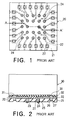
- the semiconductor device includes a carrier tape 20 having an organic insulating film 21 and wiring layers 22 formed on the organic insulating film 21.
- a material of the organic insulating film 21 may be polyimide resin or the like.
- the wiring layers 22 are formed by processing, such as etching, a metal foil of copper or the like into desired shapes. Each wiring layer 22 is formed with a region for connection to a corresponding electrode pad 31 of a semiconductor chip 30.
- the semiconductor chip 30 and the carrier tape 20 are bonded together by means of an adhesive film 23.
- a plurality of bump electrodes 24 are formed as electrode pads of the carrier tape 20 for connection to the exterior.
- a material of the bump electrode 24 may be solder or the like. As shown in Fig. 1, the bump electrodes 24 are arranged in a grid at regular pitches and distributed widely on a side of the organic insulating film 21 remote from the wiring layers 22.
- the wiring layers 22 are provided on a side of the carrier tape 20 facing the semiconductor chip 30. Each of the wiring layers 22 has one end connected to the corresponding bump electrode 24 through a via hole which is formed by filling a metal material 27 into a through hole 25.
- Through holes 26 are further formed at the carrier tape 20, and the metal material 27 is filled into the through holes 26 so as to form via holes, each for connection between the wiring layer 22 and the electrode pad 31 as inner leads.
- Each via hole is adjustable in position, when formed, relative to the electrode pad 31 and the wiring layer 22. The inner-lead connection of the electrode pad 31 and the wiring layer 22 is achieved through this via hole.
- the carrier tape 20, the adhesive film 23 and the semiconductor chip 30 are necessary for constituting the semiconductor device. Although it is not illustrated in Fig. 2, ball bumps 33 of gold are formed on the electrode pads 31.
- the carrier tape 20 is shown in Figs. 4 and 5.
- Fig. 4 shows the carrier tape 20 at a side of the wiring layers 22, that is, at a side facing the semiconductor chip 30.
- Fig. 5 shows an opposite side of the carrier tape 20.
- the carrier tape 20 is produced, for example, according to the following method:
- a two-layer base member in the form of the polyimide organic insulating film 21 and the metal foil of copper or the like is prepared.
- the organic insulating film 21 has sprocket holes 21-1 formed beforehand in any appropriate manner such as punching.
- the wiring layers 22 of desired shapes are formed on the two-layer base member so as to be properly positioned for connection to the electrode pads 31 of the semiconductor chip 30 through the ball bumps 33.
- each of the wiring layers 22 is connected to the metal material 27 at its one end.
- the other end thereof is connected to an electric-selection pad 22-1.
- the through holes 25 and 26 are formed at the organic insulating film 21 by etching, laser processing or the like as mentioned in conjunction with Fig. 2.
- the metal material 27 is filled into the through holes 25 and 26 by the electrolytic plating or the like for connection to the wiring layers 22.
- the organic insulating film 21 is etched so as to form positioning holes 21-2.
- the adhesive film 23 is set on the semiconductor chip 30.
- the single-point bonder which is used for the TAB connection, is used so as to achieve the foregoing inner-lead connection after properly positioning between the carrier tape 20 and the semiconductor chip 30 temporarily fixed with the adhesive film 23.
- Fig. 3D for bonding together the carrier tape 20 and the semiconductor chip 30 with the adhesive film 23 sandwiched therebetween, heat and pressure are applied for several seconds from a side of the carrier tape 20 or the semiconductor chip 30. At this time, bump electrodes 24 are formed on a side of the carrier tape 20 facing an external board, in a grid at the same pitch.
- the electric selection (BT) is performed in the same manner as in the normal tape carrier package (TCP), using the electric-selection pads 22-1.
- Fig. 3F after indicating an article name, using a laser beam, on a side of the semiconductor chip 30 remote from the carrier tape 20, the die or laser is used to cut unnecessary portions of the semiconductor device.
- the chip-size package-type semiconductor device can be obtained as shown in Fig. 3G.
- the chip-size package-type semiconductor device has been, in general, fabricated in the following manner:
- a size of the adhesive film 23 is limited to a size corresponding to an area defined within the electrode pads 31, that is, not corresponding to all the area of the joint surface of the semiconductor chip 30, so as to avoid overlapping the electrode pads 31.
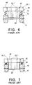
- an adhesive film tape 23' is cut into the adhesive film 23 having a required size by the use of a die assembly 40.
- the die assembly 40 comprises a die 41 and a hold-down member 42 for holding the adhesive film tape 23' onto the die 41.
- the hold-down member 42 is pressurized through a spring member 43 by an upper die 44 which is moved upwardly and downwardly by a die drive unit (not shown).
- a punch 45 is attached to an under surface of the upper die 44 in order to cut the adhesive film tape 23' in cooperation with the die 41.
- the punch 45 has a sectional size which is equal to the required size of the adhesive film 23.
- the upper die 44 and the punch 45 have a plurality of through holes 44-1 and 45-1, respectively, which are connected to each other.
- the through holes 44-1 and 45-1 are for separating the adhesive film 23 from an under surface of the punch 45 by blowing pressurized air. This is because the adhesive film 23 cut away from the adhesive film tape 23' adheres to the under surface of the punch 45.
- inlet sides of the through holes 44-1 are connected to a pressurized air supply unit (not shown).
- the semiconductor chip 30 is set onto a heating block 47 by the use of a chip positioning unit 50.
- a film positioning unit 55 and a transfer head 59 the adhesive film 23 is set onto the semiconductor chip 30 set on the heating block 47.
- the chip positioning unit 50 comprises chuck plate members 51 and 52 having chuck portions 51-1 and 52-1, respectively.
- the chuck plate member 51 is moved by a micrometer head 53.
- the chuck plate member 52 is moved by another micrometer head (not shown).
- the chuck portions 51-1 and 52-1 move so as to approach and separate from each other.
- the film positioning unit 55 comprises positioning plate members 56 and 57.
- the positioning plate member 56 has a mount portion 56-1 for mounting the adhesive film 23 and a positioning portion 56-2 for determining the position of a half of the adhesive film 23.
- the positioning plate member 57 has a positioning portion 57-2 for determining the position of another half of the adhesive film 23.
- the positioning plate member 56 is moved by a micrometer head 58.
- the positioning plate member 57 is moved by another micrometer head (not shown).
- the positioning portions 56-2 and 57-1 move so as to approach and separate from each other.
- the transfer head 59 is for transferring the adhesive film 23 from the film positioning unit 55 to the chip positioning unit 50.
- the transfer head 59 has an air chuck for holding the adhesive film 23 at an under surface thereof by the use of vacuum air.
- the transfer head 59 has a plurality of through holes 59-1 extending to the under surface of the transfer head 59. Other ends of the through holes 59-1 are connected to an air vacuum unit (not shown).
- the adhesive film 23 is set onto the semiconductor chip 30 in the manner mentioned hereinunder.
- a center positioning operation between the semiconductor chip 30 and the transfer head 59 is carried out over the heating block 47 by moving the positioning plate members 51 and 52 in a state that the positioning plate members 51 and 52 chuck the semiconductor chip 30.
- a center positioning operation between the adhesive film 23 and the transfer head 59 is carried out over the semiconductor chip 30 by moving the positioning plate members 56 and 57 in a state that the adhesive film 23 is positioned by the positioning portions 56-2 and 57-1.
- the transfer head 59 is moved downwardly and holds the adhesive film 23 at the under surface thereof by the vacuum air.
- the transfer head 59 is temporarily moved upwardly.
- the positioning plate members 56 and 57 are moved so as to separate from each other.
- the transfer head 59 is moved downwardly through a space between the positioning plate members 56 and 57 and is stopped at the position that the adhesive film 23 comes into contact with the semiconductor chip 30. Subsequently, the transfer head 59 releases the adhesive film 23 by stopping the vacuum air.
- the transfer head 59 is moved upwardly and then the adhesive film 23 is heated by the heating block 47. When the adhesive film 23 melts, the carrier tape is transferred over the semiconductor chip 30 by another transfer unit (not shown). Then, the bonding step is carried out as described in conjunction with Fig. 3C.
- the semiconductor chip 30 is molded by resin material by the use of a die unit 60.
- the die unit 60 comprises a lower side die 61 and an upper side die 62.
- the lower side die 61 has an injection hole 61-1 extending from an under surface to an upper surface for injecting melted resin material.
- two positioning pins 61-2 are attached onto the upper surface of the lower die 61.
- the upper die 62 has a cavity portion 62-1 at a center area of an under surface thereof and a guide path 62-2 for connecting between the injection hole 61-1 and the cavity portion 62-1.
- the upper die 62 further has an air vent 62-3 extending from the cavity portion 62-1 to an external area.
- a release pin 63 is inserted into the upper die 62 at a center portion thereof in order for releasing the lower die 61 from the upper die 62 after completion of the molding step.
- the molding step is carried out in a manner mentioned hereinunder.
- the melted resin material is injected through the injection hole 61-1 and guide path 62-2 into the cavity portion 62-1 that holds the semiconductor chip 30 bonded with the carrier tape 20.
- the carrier tape 20 is on the lower die 61 in order to mold the semiconductor chip 30 only.
- a plunger piston 64 is inserted into the injection hole 61-1 under pressurization.
- the melted resin material is filled into the cavity portion 62-1.
- the carrier tape 20 releases from the lower die 61 together with the semiconductor chip 30.
- the semiconductor chip 30 will be called a package hereinafter.
- the cutting step is carried out by a cut die assembly similar to that described in conjunction with Figs. 6 and 7.
- the cut die assembly comprises a die 65 and a hold-down member 66 for holding the carrier tape 20 onto the die 65.
- the hold-down member 66 is pressurized through a spring member 67 by an upper die 68 which is moved upwardly and downwardly by a die drive unit (not shown).
- a punch 69 is attached to an under surface of the upper die 68 in order to cut the carrier tape 20 in cooperation with the die 65.
- the punch 69 has a sectional size which is equal to an outline of the semiconductor chip 30 molded by the resin material.
- the upper die 68 and the punch 69 have a plurality of through holes 68-1 and 69-1, respectively, which are connected to each other.
- the through holes 68-1 and 69-1 are for holding a package 30' at an under surface of the punch 69 by vacuum air.
- inlet sides of the through holes 68-1 are connected to an air vacuum unit (not shown).
- the carrier tape 20 is held by the hold-down member 66. Subsequently, the punch 69 cuts unnecessary portion of the carrier tape 20. The punch 69 holds the package 30' by the vacuum air.
- a cutting and setting step of the adhesive film will be described.
- the cutting and setting step is carried out by a device illustrated in Fig. 13 before bonding of the carrier tape and the semiconductor chip.
- the device comprises a transfer plate 70 which is for moving a ⁇ -axis table 71.
- the transfer plate 70 is moved between a chip set position depicted at a chain line and a film set position that is illustrated by a real line.
- An X-Y table 72 is mounted on the ⁇ -axis table 71.
- the ⁇ axis means a vertical axis.
- the ⁇ -axis may be called a Z-axis.
- the ⁇ -axis table 71 is for horizontarily rotating the X-Y table 72 around a center axis thereof.
- the ⁇ -axis table 71 has an X-Y plane defined by an X-axis and a Y-axis.
- the X-Y table 72 is movable with respect to the X-axis and the Y-axis on the ⁇ -axis table 71.
- a heating block 74 is mounted on the X-Y table 72 through a support member 74.
- the heating block 73 comprises a heater and an air chuck mechanism for holding the semiconductor chip 30 by vacuum air.
- the heating block 73 has a through hole 73-1 which is connected to an air vacuum unit (not shown).
- a die 76 is formed at an upper side of the support frame 75, namely, over the heating block 73.
- the die 76 serves as a table for supporting the adhesive film tape 23' of a sheet-shape.
- a hold-down plate 77 is installed via guide members 78.
- the hold-down plate 77 is slidable upwardly and downwardly along the guide members 78.
- the adhesive film tape 23' is held on the die 76 by the hold-down plate 77 slid downwardly.
- An up-down plate 79 is combined with the hold-down plate 77 and is slidable upwardly and downwardly along the guide members 78.
- the up-down plate 79 is provided with a pair of first air cylinder mechanisms 80. Driving shafts 80-1 of the first air cylinder mechanisms 80 are fixed to the hold-down plate 77.
- a support plate 81 is attached to upper ends of the guide members 78.
- the support plate 81 is provided with a second air cylinder mechanism 82.
- a driving shaft 82-1 of the second air cylinder mechanism 82 is fixed to the up-down plate 79.
- the up-down plate 79 is further provided with a punch 83 at a lower side and a center portion thereof.
- the punch 83 has a sectional size which is equal to a required size of the adhesive film.
- the punch 83 extends downwardly and passes through a center portion of the hold-down plate 77. Accordingly, the punch 83 moves together with the up-down plate 79.
- the punch 83 comprises an air chuck mechanism for holding the adhesive film cut away from the adhesive film tape 23' by the vacuum air.
- the punch 83 has a through hole 83-1 connected to a vacuum air unit (not shown). It is desirable that the under surface of the punch 83 is treated by coating such as teflon coating, TiN coating, or the like, in order to improve separation characteristic between the adhesive film and the punch 83.
- the hold-down plate 77 moves up and down together with the up-down plate 79.
- the first air cylinder mechanisms 80 are driven, only the hold-down plate 77 moves up and down.
- the adhesive film tape 23' is fed by a tape feed unit (not shown) in a vertical direction on a surface of the drawing.
- the adhesive film tape 23' may be rolled in a roll-shape.
- the transfer plate 70 is positioned at the chip set position. At this position, the semiconductor chip 30 is set onto the heating block 73. The semiconductor chip 30 is held by the air chuck mechanism of the heating block 73. Then, the transfer plate 70 moves from the chip set position to the film set position.
- the semiconductor chip 30 is positioned so that the semiconductor chip 30 is present just under an opening of the die 76 and that a center of the semiconductor chip 30 is coincident with a center of the punch 83.
- the adhesive film tape 23' is held on the upper surface of the die 76 by the hold-down plate 77.
- the punch 83 is moved downwardly and cuts the adhesive film away from the adhesive film tape 23'.
- the punch 83 holds the adhesive film cut away from the adhesive film tape 23' at the under surface thereof by the vacuum air and continues downward movement.
- the downward movement of the punch 83 is stopped.
- a driving force of the second air cylinder mechanism 82 is reduced by reducing an air pressure thereof.
- the punch 83 releases the adhesive film by stopping the vacuum air.
- the adhesive film is set onto the semiconductor chip 30.
- the adhesive film is melted by the heating block 73. As a result, the adhesive film temporarily adheres to the semiconductor chip 30. Then, the semiconductor chip 30 is transferred to another device and is bonded to the carrier tape in the manner mentioned in conjunction with Fig. 3.
- the adhesive film tape 23' is treated in the form of the tape-shape or the roll-shape, handling becomes easy. Further, since the punch 83 carries out the punching and the holding of the adhesive film, the adhesive film is held by the punch 83 without deviation of position. This means that the adhesive film is set onto the semiconductor chip in high accuracy by carrying out only the positioning of the semiconductor chip against the punch 83.
- the description will proceed to a molding step of the semiconductor chip 30 according to the present invention.
- the semiconductor chip 30 has been bonded to the carrier tape 20.
- the molding step is carried out in the manner of a screen printing by the use of a metal mask 90.
- the metal mask 90 has a thickness which is a little more thicker than that of the semiconductor chip 30 and has an opening 90-1 which is narrower than the carrier tape 20 and which is capable of receiving the semiconductor chip 30.
- the metal mask 90 is held in a support table 91 having a rectangular recessed portion.
- a pair of positioning pins 92 are attached to a bottom surface of the recessed portion.
- the positioning pins 92 are symmetrical with respect to a center of the recessed portion.
- the carrier tape 20 has a pair of positioning holes 20-1 at positions which are correspond to the positioning pins 92.
- the metal mask 90 has a pair of positioning holes 90-2 at positions which are correspond to the positioning pins 92.
- a pair of mask holders 93 are attached to both sides of the support table 91 in order to fix the metal mask 90 to the support table 91.
- the molding step of the semiconductor chip 30 is carried out in the following manner. At first, by inserting the positioning pins 92 into the positioning holes 20-1, the semiconductor chip 30 is set into the recessed portion in a state that the carrier tape 20 is close to the bottom surface of the recessed portion. The metal mask 90 is set into the recessed portion by inserting the positioning pins 92 into the positioning holes 90-2. Then, the metal mask 90 is fixed by the mask holders 93 to the support table 91. In this state, melt resin material is injected into the opening 90-1. The melt resin material brimmed over the opening 90-1 is scraped off by a squeegee (not shown). After solidification of the resin material, the metal mask 90 is removed from the support table 91. Thus, it is possible to obtain the semiconductor chip molded by the resin material.
- the semiconductor chip molded by the resin material will be called a package hereinafter.
- the metal mask 90 is made of, for example, stainless steel because it has superior release characteristic. It is desirable to prepare a plurality of metal masks which are different in thickness and in size of opening 90-1 according to the size of the semiconductor chip 30.
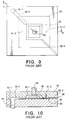
- the metal mask 90 is inexpensive because it is no need a complex shape that is illustrated in Figs. 9 and 10. Since the semiconductor chip 30 is molded by the screen printing in a state that the carrier tape 20 is fixed by the mask holders 93, dispersion of thickness in the package can be improved.
- the semiconductor chip 30 can be molded in high accuracy because it is positioned precisely on the basis of the positioning pins 92.
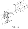
- a YAG laser unit is used for the cutting step.
- the YAG laser unit comprises a YAG laser generating unit 95 for generating a laser beam.
- a fourth harmonic wave is used as the laser beam as will later be described in detail.
- the laser beam is projected through a dichroic mirror 96, an attenuator 97, a first galvano mirror 98, a second galvano mirror 99, and F ⁇ lens 100 to the carrier tape 20.
- the first galvano mirror 98 is for scanning the laser beam in an X-axis direction on the carrier tape 20 and is driven by a first drive unit 101.
- the second galvano mirror 99 is for scanning the laser beam in a Y-axis direction on the carrier tape 20 and is driven by a second drive unit 102.
- the laser beam is projected to the carrier tape 20 so as to draw a square having the same size as the package.
- the size of the square is predetermined as a cutting size defined by a cutting line because the size of the package is known in advance.
- a CCD camera 103 is for carrying out the positioning of the carrier tape 20 by the use of a light path for the laser beam.
- a reflection mirror 104 is used.
- the carrier tape 20 integrated with the package is held by a hold table which will shortly be described.
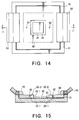
- the carrier tape 20 has two alignment marks 20-2a and 20-2b at the opposite side opposite to the side of the wiring layer described in conjunction with Figs. 4 and 5.
- the alignment marks 20-2a and 20-2b suffice for determining the cutting line of the square illustrated by a chain line. It is desirable that the alignment marks 20-2a and 20-2b locate at corners of the square.
- Fig. 18 the package is depicted at 30'.
- the carrier tape 20 is held by a carrier tape holder 105.
- the carrier tape holder 105 is set on a hold table 106.
- the hold table 106 is mounted on an X-Y-Z- ⁇ table 107.
- the X-Y-Z- ⁇ table 107 is movable in X-axis, Y-axis, and Z-axis directions, and is rotatable in a ⁇ direction.
- the X-Y-Z- ⁇ table 107 is horizontally rotatable. All of directions are illustrated in Fig. 16. Since such an X-Y-Z- ⁇ table is well known in the art, a detailed description is omitted.
- Two positioning pins 106-1 are attached onto the hold table 106 for positioning the carrier tape 20 by the use of the positioning holes 20-1. Namely, the carrier tape holder 105 is set on the hold table 106 by inserting the positioning pins 106-1 into the positioning holes 20-1. In this state, the hold table 106 holds the package 30' by air chucking by the use of vacuum air through a through hole 109. An inlet side of the through hole 109 is connected to an air vacuum unit (not shown).
- the carrier tape 20 is positioned at a predetermined area so that the carrier tape 20 comes into sight of the CCD camera 103.
- the CCD camera 103 carries out a search operation of the alignment marks 20-2a and 20-2b in a manner of image processing well known in the art.
- the alignment marks 20-2a and 20-2b are detected, one of the alignment marks 20-2a and 20-2b is determined as the starting point of the laser beam projection.
- the laser beam is projected by the YAG laser unit so as to draw the cutting line which passes through the alignment marks 20-2a and 20-2b as illustrated in Fig. 17 by the chain line.
- the carrier tape 20 is cut into the same size as the package 30'.
- a reference beam light is projected, at first, to the starting point of the laser beam projection. Then, the carrier tape 20 is positioned by the X-Y-Z- ⁇ table 107 so that one of the alignment marks 20-2a and 20-2b coincides with a projection point of the reference beam light. Next, the reference beam light is projected to another projection point that another one of the alignment marks 20-2a and 20-2b must be positioned. Then, the carrier tape 20 is rotated by the X-Y-Z- ⁇ table 107 so that other one of the alignment marks 20-2a and 20-2b coincides with the other projection point of the reference beam light. Next, the laser beam is projected by the YAG laser unit so as to draw the cutting line which passes through the alignment marks 20-2a and 20-2b. In the other manner, the image processing is used.
- the cutting size of the carrier tape 20 can be voluntarily changed because a rotation angle of the first and the second galvano mirrors 98 and 99 can be voluntarily adjusted. Since the cutting step is carried out by non-contact, the carrier tape 20 no receive mechanical stress.
- the YAG laser generating unit 95 comprises an YAG laser oscillator 110, a second harmonic generation element 111, and a fourth harmonic generation element 112 in order to generate the fourth harmonic wave mentioned in conjunction with Fig. 16.
- the YAG laser oscillator 110 generates a laser beam of a first stage having a wavelength of 1.06 ( ⁇ m).
- the second harmonic generation element 111 receives the laser beam of the first stage and generates a laser beam of a second stage having a wavelength of 0.53 ( ⁇ m).
- the fourth harmonic generation element 112 receives the laser beam of the second stage and generates a laser beam having a wavelength of 0.266 ( ⁇ m).
- the second harmonic generation element 111 is implemented by a KTP element while the fourth harmonic generation element 112 is implemented by a ⁇ BBO element.
- ultraviolet light having the wavelength of 0.266 ( ⁇ m) is used.
- Such the ultraviolet light has a high absorption rate of laser energy and has a characteristic that a heating value in the carrier tape 20 is restrained. This is because diffusion of the energy caused by thermal conduction is restrained because the laser beam is projected in the form of a pulse wave. As a result, the carrier tape 20 has a reduced thermal stress.
Landscapes
- Wire Bonding (AREA)
- Encapsulation Of And Coatings For Semiconductor Or Solid State Devices (AREA)
- Container, Conveyance, Adherence, Positioning, Of Wafer (AREA)
Applications Claiming Priority (2)
| Application Number | Priority Date | Filing Date | Title |
|---|---|---|---|
| JP271449/95 | 1995-10-19 | ||
| JP7271449A JP2666788B2 (ja) | 1995-10-19 | 1995-10-19 | チップサイズ半導体装置の製造方法 |
Publications (2)
| Publication Number | Publication Date |
|---|---|
| EP0769812A2 true EP0769812A2 (fr) | 1997-04-23 |
| EP0769812A3 EP0769812A3 (fr) | 1998-10-21 |
Family
ID=17500189
Family Applications (1)
| Application Number | Title | Priority Date | Filing Date |
|---|---|---|---|
| EP96116769A Withdrawn EP0769812A3 (fr) | 1995-10-19 | 1996-10-18 | Méthode de fabrication de boítiers semi-conducteurs à largeur de puce |
Country Status (5)
| Country | Link |
|---|---|
| US (1) | US5759873A (fr) |
| EP (1) | EP0769812A3 (fr) |
| JP (1) | JP2666788B2 (fr) |
| KR (1) | KR100203603B1 (fr) |
| CN (1) | CN1107972C (fr) |
Cited By (1)
| Publication number | Priority date | Publication date | Assignee | Title |
|---|---|---|---|---|
| WO1999035690A1 (fr) * | 1998-01-09 | 1999-07-15 | Siemens Aktiengesellschaft | Procede pour produire un composant a semi-conducteur et composant a semi-conducteur obtenu a l'aide dudit procede |
Families Citing this family (30)
| Publication number | Priority date | Publication date | Assignee | Title |
|---|---|---|---|---|
| TW281795B (fr) * | 1994-11-30 | 1996-07-21 | Sharp Kk | |
| KR100186333B1 (ko) * | 1996-06-20 | 1999-03-20 | 문정환 | 칩 사이즈 반도체 패키지 및 그 제조방법 |
| US6230719B1 (en) | 1998-02-27 | 2001-05-15 | Micron Technology, Inc. | Apparatus for removing contaminants on electronic devices |
| US5972234A (en) * | 1998-04-06 | 1999-10-26 | Taiwan Semiconductor Manufacturing Co., Ltd. | Debris-free wafer marking method |
| US6472726B1 (en) | 1998-07-28 | 2002-10-29 | Seiko Epson Corporation | Semiconductor device and method of fabrication thereof, semiconductor module, circuit board, and electronic equipment |
| US6479887B1 (en) | 1998-08-31 | 2002-11-12 | Amkor Technology, Inc. | Circuit pattern tape for wafer-scale production of chip size semiconductor packages |
| US6428641B1 (en) * | 1998-08-31 | 2002-08-06 | Amkor Technology, Inc. | Method for laminating circuit pattern tape on semiconductor wafer |
| JP3816253B2 (ja) * | 1999-01-19 | 2006-08-30 | 富士通株式会社 | 半導体装置の製造方法 |
| JP3504543B2 (ja) | 1999-03-03 | 2004-03-08 | 株式会社日立製作所 | 半導体素子の分離方法およびその装置並びに半導体素子の搭載方法 |
| US6181569B1 (en) | 1999-06-07 | 2001-01-30 | Kishore K. Chakravorty | Low cost chip size package and method of fabricating the same |
| US6210522B1 (en) | 1999-06-15 | 2001-04-03 | Lexmark International, Inc. | Adhesive bonding laminates |
| US6361146B1 (en) | 1999-06-15 | 2002-03-26 | Lexmark International, Inc. | Adhesive bonding laminates |
| US6322903B1 (en) | 1999-12-06 | 2001-11-27 | Tru-Si Technologies, Inc. | Package of integrated circuits and vertical integration |
| JP4128319B2 (ja) * | 1999-12-24 | 2008-07-30 | 株式会社新川 | マルチチップボンディング方法及び装置 |
| CH695407A5 (de) * | 2000-07-03 | 2006-04-28 | Esec Trading Sa | Verfahren und Einrichtung zur Montage von Halbleiterchips auf einem flexiblen Substrat. |
| JP3619773B2 (ja) * | 2000-12-20 | 2005-02-16 | 株式会社ルネサステクノロジ | 半導体装置の製造方法 |
| EP1282162A3 (fr) * | 2001-08-03 | 2005-02-02 | Matsushita Electric Industrial Co., Ltd. | Procédé et appareil pour la fabrication d'empaquetages pour semi-conducteurs |
| JP2003330041A (ja) * | 2002-05-10 | 2003-11-19 | Sharp Corp | 半導体装置及びそれを備えた表示パネルモジュール |
| US7416922B2 (en) * | 2003-03-31 | 2008-08-26 | Intel Corporation | Heat sink with preattached thermal interface material and method of making same |
| US6987671B2 (en) * | 2003-06-26 | 2006-01-17 | Intel Corporation | Composite thermal interface devices and methods for integrated circuit heat transfer |
| US7527090B2 (en) * | 2003-06-30 | 2009-05-05 | Intel Corporation | Heat dissipating device with preselected designed interface for thermal interface materials |
| US7571541B2 (en) * | 2005-01-10 | 2009-08-11 | Silverbrook Research Pty Ltd | Method of producing an inkjet printhead for an inkjet printer with a print engine controller |
| JP4975605B2 (ja) * | 2007-12-26 | 2012-07-11 | 東京エレクトロン株式会社 | 処理システム、処理システムの制御方法およびソフトウェアのバージョンアップ方法 |
| JP5557352B2 (ja) * | 2012-04-20 | 2014-07-23 | Necエンジニアリング株式会社 | シート切断装置、チップ製造装置、シート切断方法、チップ製造方法及びシート切断プログラム |
| US10186458B2 (en) * | 2012-07-05 | 2019-01-22 | Infineon Technologies Ag | Component and method of manufacturing a component using an ultrathin carrier |
| US9922935B2 (en) | 2014-09-17 | 2018-03-20 | Samsung Electronics Co., Ltd. | Semiconductor package and method of fabricating the same |
| KR20160032958A (ko) | 2014-09-17 | 2016-03-25 | 삼성전자주식회사 | 반도체 패키지 및 이의 제조 방법 |
| CN104960349B (zh) * | 2015-06-11 | 2021-08-06 | 苏州海博智能系统有限公司 | 一种电子显示屏印刷片材的处理设备 |
| CN104942877B (zh) * | 2015-06-18 | 2021-08-13 | 苏州海博智能系统有限公司 | 一种电子显示屏印刷片材的处理设备 |
| KR102036335B1 (ko) * | 2019-07-09 | 2019-10-24 | (주)에이티에스 | Cof 2중 타발장치 |
Family Cites Families (8)
| Publication number | Priority date | Publication date | Assignee | Title |
|---|---|---|---|---|
| JPS60224254A (ja) * | 1984-04-20 | 1985-11-08 | Hitachi Yonezawa Denshi Kk | リ−ドフレ−ム切断方法 |
| US5049434A (en) * | 1984-04-30 | 1991-09-17 | National Starch And Chemical Investment Holding Corporation | Pre-patterned device substrate device-attach adhesive transfer system |
| JPS62111825A (ja) * | 1985-11-06 | 1987-05-22 | Fuji Kikai Seizo Kk | キヤリヤテ−プから電子部品を取り出す方法 |
| JPH0787277B2 (ja) * | 1987-03-25 | 1995-09-20 | ティーディーケイ株式会社 | 表面実装部品の基板搭載方法 |
| JPS6443458A (en) * | 1987-08-11 | 1989-02-15 | Nitto Denko Corp | Stick cutter for tacky tape with respect to thin board |
| JPH03250634A (ja) * | 1990-02-28 | 1991-11-08 | Fujitsu Ltd | 半導体装置の製造方法 |
| JPH06192630A (ja) * | 1992-12-25 | 1994-07-12 | Sony Corp | カード型半導体装置のパネルへの両面接着テープ接着 用セパレータ |
| JP2570123B2 (ja) * | 1993-07-13 | 1997-01-08 | 日本電気株式会社 | 半導体装置及びその製造方法 |
-
1995
- 1995-10-19 JP JP7271449A patent/JP2666788B2/ja not_active Expired - Fee Related
-
1996
- 1996-10-17 US US08/733,207 patent/US5759873A/en not_active Expired - Fee Related
- 1996-10-18 EP EP96116769A patent/EP0769812A3/fr not_active Withdrawn
- 1996-10-19 CN CN96121929A patent/CN1107972C/zh not_active Expired - Fee Related
- 1996-10-19 KR KR1019960046982A patent/KR100203603B1/ko not_active Expired - Fee Related
Cited By (2)
| Publication number | Priority date | Publication date | Assignee | Title |
|---|---|---|---|---|
| WO1999035690A1 (fr) * | 1998-01-09 | 1999-07-15 | Siemens Aktiengesellschaft | Procede pour produire un composant a semi-conducteur et composant a semi-conducteur obtenu a l'aide dudit procede |
| DE19800566A1 (de) * | 1998-01-09 | 1999-07-15 | Siemens Ag | Verfahren zum Herstellen eines Halbleiterbauelementes und ein derart hergestelltes Halbleiterbauelement |
Also Published As
| Publication number | Publication date |
|---|---|
| JP2666788B2 (ja) | 1997-10-22 |
| CN1107972C (zh) | 2003-05-07 |
| KR100203603B1 (ko) | 1999-07-01 |
| KR970024041A (ko) | 1997-05-30 |
| JPH09115950A (ja) | 1997-05-02 |
| CN1155162A (zh) | 1997-07-23 |
| US5759873A (en) | 1998-06-02 |
| EP0769812A3 (fr) | 1998-10-21 |
Similar Documents
| Publication | Publication Date | Title |
|---|---|---|
| US5759873A (en) | Method of manufacturing chip-size package-type semiconductor device | |
| KR100330937B1 (ko) | 복수의 초소형 전자소자를 리드변형을 이용하여 접속하는 방법 및 장치 | |
| EP0704899B1 (fr) | Procédé de fabrication d'un boítier pour dispositif semi-conducteur de la taille d'une puce | |
| US6543131B1 (en) | Microelectronic joining processes with temporary securement | |
| US5427301A (en) | Ultrasonic flip chip process and apparatus | |
| JP3022949B2 (ja) | マイクロエレクトロニクス素子の実装構造及びその製造方法 | |
| JP2925074B2 (ja) | Loc型半導体チップパッケージ及びその製造方法 | |
| US5462626A (en) | Method of bonding an external lead and a tool therefor | |
| JP4696110B2 (ja) | 電子部品の実装方法及び電子部品実装装置 | |
| JPH0779152B2 (ja) | フリップチップ型半導体装置の実装方法 | |
| JP3175737B2 (ja) | 電子部品実装装置および電子部品実装方法 | |
| US12568589B2 (en) | Method of bonding column type deposits | |
| US20250132286A1 (en) | Semiconductor packaging method, semiconductor assembly component and electronic device | |
| CN121985850A (en) | Bonding device and bonding method implemented by the bonding device | |
| JP3086125B2 (ja) | 半導体チップへのバンプ形成方法および装置 | |
| JP3233137B2 (ja) | 電子部品実装装置および電子部品実装方法 | |
| JP2837145B2 (ja) | チップ部品と基板との接続方法および接続装置 | |
| KR20240027705A (ko) | 땜납 범프 형성 방법 | |
| JP3351372B2 (ja) | 電子部品実装装置および電子部品実装方法 | |
| JP3086124B2 (ja) | ボンディング用バンプの形成方法および装置 | |
| JP2000150581A (ja) | 半導体装置およびその製造方法並びにそれに使用されるボンディング装置 |
Legal Events
| Date | Code | Title | Description |
|---|---|---|---|
| PUAI | Public reference made under article 153(3) epc to a published international application that has entered the european phase |
Free format text: ORIGINAL CODE: 0009012 |
|
| AK | Designated contracting states |
Kind code of ref document: A2 Designated state(s): DE FR GB |
|
| PUAL | Search report despatched |
Free format text: ORIGINAL CODE: 0009013 |
|
| AK | Designated contracting states |
Kind code of ref document: A3 Designated state(s): DE FR GB |
|
| 17P | Request for examination filed |
Effective date: 19980914 |
|
| RAP1 | Party data changed (applicant data changed or rights of an application transferred) |
Owner name: NEC ELECTRONICS CORPORATION |
|
| STAA | Information on the status of an ep patent application or granted ep patent |
Free format text: STATUS: THE APPLICATION HAS BEEN WITHDRAWN |
|
| 18W | Application withdrawn |
Effective date: 20030901 |