EP0769831A1 - Halbleiterlaser und Verfahren zur Herstellung des Halbleiterlasers - Google Patents
Halbleiterlaser und Verfahren zur Herstellung des Halbleiterlasers Download PDFInfo
- Publication number
- EP0769831A1 EP0769831A1 EP96106308A EP96106308A EP0769831A1 EP 0769831 A1 EP0769831 A1 EP 0769831A1 EP 96106308 A EP96106308 A EP 96106308A EP 96106308 A EP96106308 A EP 96106308A EP 0769831 A1 EP0769831 A1 EP 0769831A1
- Authority
- EP
- European Patent Office
- Prior art keywords
- layer
- conductivity type
- cladding layer
- upper cladding
- ridge structure
- Prior art date
- Legal status (The legal status is an assumption and is not a legal conclusion. Google has not performed a legal analysis and makes no representation as to the accuracy of the status listed.)
- Withdrawn
Links
Images



Classifications
-
- H—ELECTRICITY
- H01—ELECTRIC ELEMENTS
- H01S—DEVICES USING THE PROCESS OF LIGHT AMPLIFICATION BY STIMULATED EMISSION OF RADIATION [LASER] TO AMPLIFY OR GENERATE LIGHT; DEVICES USING STIMULATED EMISSION OF ELECTROMAGNETIC RADIATION IN WAVE RANGES OTHER THAN OPTICAL
- H01S5/00—Semiconductor lasers
- H01S5/20—Structure or shape of the semiconductor body to guide the optical wave ; Confining structures perpendicular to the optical axis, e.g. index or gain guiding, stripe geometry, broad area lasers, gain tailoring, transverse or lateral reflectors, special cladding structures, MQW barrier reflection layers
- H01S5/22—Structure or shape of the semiconductor body to guide the optical wave ; Confining structures perpendicular to the optical axis, e.g. index or gain guiding, stripe geometry, broad area lasers, gain tailoring, transverse or lateral reflectors, special cladding structures, MQW barrier reflection layers having a ridge or stripe structure
- H01S5/223—Buried stripe structure
- H01S5/2231—Buried stripe structure with inner confining structure only between the active layer and the upper electrode
-
- H—ELECTRICITY
- H01—ELECTRIC ELEMENTS
- H01S—DEVICES USING THE PROCESS OF LIGHT AMPLIFICATION BY STIMULATED EMISSION OF RADIATION [LASER] TO AMPLIFY OR GENERATE LIGHT; DEVICES USING STIMULATED EMISSION OF ELECTROMAGNETIC RADIATION IN WAVE RANGES OTHER THAN OPTICAL
- H01S5/00—Semiconductor lasers
- H01S5/30—Structure or shape of the active region; Materials used for the active region
- H01S5/32—Structure or shape of the active region; Materials used for the active region comprising PN junctions, e.g. hetero- or double- heterostructures
- H01S5/321—Structure or shape of the active region; Materials used for the active region comprising PN junctions, e.g. hetero- or double- heterostructures having intermediate bandgap layers
-
- H—ELECTRICITY
- H01—ELECTRIC ELEMENTS
- H01S—DEVICES USING THE PROCESS OF LIGHT AMPLIFICATION BY STIMULATED EMISSION OF RADIATION [LASER] TO AMPLIFY OR GENERATE LIGHT; DEVICES USING STIMULATED EMISSION OF ELECTROMAGNETIC RADIATION IN WAVE RANGES OTHER THAN OPTICAL
- H01S5/00—Semiconductor lasers
- H01S5/20—Structure or shape of the semiconductor body to guide the optical wave ; Confining structures perpendicular to the optical axis, e.g. index or gain guiding, stripe geometry, broad area lasers, gain tailoring, transverse or lateral reflectors, special cladding structures, MQW barrier reflection layers
- H01S5/2054—Methods of obtaining the confinement
- H01S5/2081—Methods of obtaining the confinement using special etching techniques
- H01S5/209—Methods of obtaining the confinement using special etching techniques special etch stop layers
-
- H—ELECTRICITY
- H01—ELECTRIC ELEMENTS
- H01S—DEVICES USING THE PROCESS OF LIGHT AMPLIFICATION BY STIMULATED EMISSION OF RADIATION [LASER] TO AMPLIFY OR GENERATE LIGHT; DEVICES USING STIMULATED EMISSION OF ELECTROMAGNETIC RADIATION IN WAVE RANGES OTHER THAN OPTICAL
- H01S5/00—Semiconductor lasers
- H01S5/30—Structure or shape of the active region; Materials used for the active region
- H01S5/32—Structure or shape of the active region; Materials used for the active region comprising PN junctions, e.g. hetero- or double- heterostructures
- H01S5/323—Structure or shape of the active region; Materials used for the active region comprising PN junctions, e.g. hetero- or double- heterostructures in AIIIBV compounds, e.g. AlGaAs-laser, InP-based laser
- H01S5/32308—Structure or shape of the active region; Materials used for the active region comprising PN junctions, e.g. hetero- or double- heterostructures in AIIIBV compounds, e.g. AlGaAs-laser, InP-based laser emitting light at a wavelength less than 900 nm
- H01S5/32316—Structure or shape of the active region; Materials used for the active region comprising PN junctions, e.g. hetero- or double- heterostructures in AIIIBV compounds, e.g. AlGaAs-laser, InP-based laser emitting light at a wavelength less than 900 nm comprising only (Al)GaAs
-
- Y—GENERAL TAGGING OF NEW TECHNOLOGICAL DEVELOPMENTS; GENERAL TAGGING OF CROSS-SECTIONAL TECHNOLOGIES SPANNING OVER SEVERAL SECTIONS OF THE IPC; TECHNICAL SUBJECTS COVERED BY FORMER USPC CROSS-REFERENCE ART COLLECTIONS [XRACs] AND DIGESTS
- Y10—TECHNICAL SUBJECTS COVERED BY FORMER USPC
- Y10S—TECHNICAL SUBJECTS COVERED BY FORMER USPC CROSS-REFERENCE ART COLLECTIONS [XRACs] AND DIGESTS
- Y10S438/00—Semiconductor device manufacturing: process
- Y10S438/955—Melt-back
Definitions
- the present invention relates to a semiconductor laser including a ridge structure and a method of fabricating the semiconductor laser.
- Figure 3 is a perspective view illustrating a prior art semiconductor laser.
- reference numeral 1 designates an n type GaAs semiconductor substrate having a (100) surface orientation.
- An active layer 3 having an effective band gap energy smaller than that of the lower cladding layer 2 is disposed on the lower cladding layer 2.
- a p type Al y Ga 1-y As (y 0.7) etch stopping layer 5 having a thickness of about 200 ⁇ is disposed on the first upper cladding layer 4.
- a p type Al x Ga 1-x As (x 0.5) second upper cladding layer 6 having a thickness of 1.0 ⁇ 2.0 ⁇ m is disposed on a center part of the etch stopping layer 5.
- a p type GaAs first contact layer 7 having a thickness of 0.5 ⁇ 1 ⁇ m is disposed on the second upper cladding layer 6.
- the second upper cladding layer 6 and the first contact layer 7 form a stripe-shaped ridge structure 9 extending in the longitudinal direction of the resonator of the semiconductor laser (hereinafter referred to as resonator length direction), and the cross section of the ridge structure 9 in a plane perpendicular to the resonator length direction is a reverse mesa.
- An n type current blocking layer 12 comprising a material having an effective band gap energy smaller than that of the active layer is disposed on the etch stopping layer 5, contacting both sides of the ridge structure 9.
- the current blocking layer 12 comprises n type GaAs.
- a p type GaAs second contact layer 13 having a thickness of 2 ⁇ 3 ⁇ m is disposed on the first contact layer 7 and on the current blocking layer 12.
- a p side electrode 14 is disposed on the second contact layer 13 and an n side electrode 15 is disposed on the rear surface of the substrate 1.
- Reference numeral 9c designates a constricted part of the ridge structure 9.
- the stripe-shaped ridge structure 9 will be described in more detail.
- region adjacent to the ridge structure 9 and covered with the n type GaAs current blocking layer 12 pn junctions are produced between the n type current blocking layer 12 and the p type first upper cladding layer 4 and between the n type current blocking layer 12 and the p type second contact layer 13. Therefore, even when a forward bias voltage is applied across the p side electrode and the n side electrode, since pnp junctions are produced in the region other than the ridge structure 9 and the voltage is applied in the reverse bias direction in this region, no current flows in this region. That is, the n type GaAs current blocking layer 12 blocks current literally.
- the n type GaAs current blocking layer 12 has the property of absorbing laser light produced in the quantum well active layer 3 because the band gap energy of GaAs is smaller than the effective band gap energy of the active layer 3.
- the laser light is subjected to strong absorption at the both sides of the ridge structure 9, so that the laser light is concentrated only in the vicinity of the ridge structure 9.
- the horizontal transverse mode which is an important operating characteristic of the semiconductor laser, has a single peak with high stability.
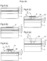
- Figures 4(a)-4(e) are cross-sectional views illustrating process steps in a method of fabricating the semiconductor laser shown in figure 3.
- the same reference numerals as those in figure 3 designate the same or corresponding parts.
- Reference numeral 8 designates a mask for forming the ridge structure 9.
- Figure 5 is an enlarged perspective view of a part A of the structure shown in figure 4(c).
- Reference numeral 5a designates a (100) surface of the etch stopping layer 5 that is exposed by etching.
- Reference numeral 9a designates an upper part of a side surface of the ridge structure 9 in the resonator length direction (hereinafter referred to as ridge side surface).
- the upper part 9a of the ridge side surface is in a ( 11 ⁇ 1)A plane.
- Reference numeral 9b designates a lower part of the ridge side surface, and it is in a plane between the ( 11 ⁇ 1)A plane and the (100) plane.
- an n type GaAs semiconductor wafer 1 having a (100) surface orientation is prepared.
- the n type lower cladding layer 2 On the (100) surface of the semiconductor wafer 1, the n type lower cladding layer 2, the active layer 3, the p type first upper cladding layer 4, the p type etch stopping layer 5, a p type second upper cladding layer 6, and the p type first contact layer 7 are epitaxially grown in this order.
- these layers are grown by MOCVD (Metal organic Chemical Vapor Deposition).
- Figure 4(a) shows a cross-sectional view of the wafer after the epitaxial growth.
- an insulating film such as Si 3 N 4 or SiO 2 , is deposited over the p type first contact layer 7 and patterned to form a stripe-shaped mask 8 extending in a direction that provides a stripe-shaped ridge structure having a reverse mesa cross section in the first contact layer 7 and the second upper cladding layer 6 (hereinafter referred to as a reverse mesa direction), for example, the [011] direction.
- the width of the mask 8 in the direction perpendicular to the resonator length direction (hereinafter referred to as resonator width direction) is about 8 ⁇ m.
- the first contact layer 7 and the second upper cladding layer 6 are etched until the etching front reaches the etch stopping layer 5, producing a stripe-shaped ridge structure 9 having a reverse mesa cross section (hereinafter referred to as a reverse mesa ridge structure).
- a mixture of tartaric acid and hydrogen peroxide that is generally used as an etchant for forming a ridge is employed.
- Whether the etching front reaches the etch stopping layer 5 is detected by visually observing the change of reflected light at the surface of the wafer that corresponds to the change of the layer at the surface. More specifically, when the etching front reaches the etch stopping layer 5, the interference color of the reflected light disappears. So, the wafer is taken out of the etchant the moment the interference color disappears, followed by washing of the wafer with water.
- the reverse mesa ridge structure shown in figure 5 is fabricated in the above-described process steps.
- the ridge structure 9 does not have a perfect mesa shape in which the width in the resonator width direction (hereinafter referred to as ridge width) is tapered toward the etch stopping layer 5.
- the ridge structure 9 has a constricted part 9c parallel to the stripe direction of the ridge at the lower part in the vicinity of the etch stopping layer 5.
- the opposed side walls of the ridge structure 9 protrude toward the center of the ridge structure.
- the ridge width is tapered from the top of the ridge to the constricted part 9c and then it is increased from the constricted part 9c to the bottom of the ridge contacting the etch stopping layer 5.
- the side surface 9b of the lower part of the ridge makes an obtuse angle with the surface of the etch stopping layer 5 that is exposed by the above-described etching process.
- the ridge structure 9 shown in figure 5 is formed. Since the etching rate for making the (100) plane, i.e., the etching rate in the direction perpendicular to the (100) plane, is high, when the etching front reaches the etch stopping layer 5, the etching for making the ( 11 ⁇ 1) plane which provides a side surface of a perfect reverse mesa ridge structure is insufficient. As a result, a transient plane between the (100) plane and a plane producing the side surface of the reverse mesa ridge structure 9, for example, a plane between the (100) plane and the ( 11 ⁇ 1) plane, is produced at the lower part 9b of the side surface of the ridge structure 9.
- the n type GaAs current blocking layer 12 is grown on the etch stopping layer 5 to bury the ridge structure 9. Since the mask 8 serves as a mask for the crystal growth, no crystal growth occurs on the ridge structure 9.
- the p type GaAs second contact layer 13 is grown as shown in figure 4(e). Finally, the n side electrode 15 and the p side electrode 14 are produced on the rear surface of the semiconductor substrate 1 and on the p type GaAs second contact layer 13, respectively, and the wafer is cleaved perpendicular to the stripe direction of the ridge structure 9 to produce resonator facets (not shown), completing the semiconductor laser shown in figure 3.
- the reverse mesa ridge structure 9 of the prior art semiconductor laser is formed by selectively etching the p type second upper cladding layer 6 using the stripe-shaped mask 8 until the etch stopping layer 5 is exposed.
- the ridge width at the bottom of the ridge structure 9 and proximate to the active layer 3 (hereinafter referred to as ridge bottom width), i.e., the ridge width at the boundary between the ridge structure 9 and the etch stopping layer 5, is very important for transverse mode control.
- the ridge bottom width is wide, a higher mode easily occurs, resulting in laser light having multiple peaks. Therefore, the ridge bottom width must be controlled precisely to be narrower than 4 ⁇ m.
- the ridge structure 9 does not have a perfect reverse mesa shape.
- the ridge structure has the constricted part 9c parallel to the stripe direction of the ridge at the lower part in the vicinity of the etch stopping layer 5, and the ridge width is increased from the constricted part 9c toward the etch stopping layer 5. Therefore, the width of the constricted part 9c is narrowest in the ridge structure 9, that is, the narrowest ridge width is not at the bottom of the ridge structure 9.
- the ridge bottom width is reduced to less than 4 ⁇ m
- the ridge width of the constricted part 9c is also reduced, and the resistance at that part is significantly increased, resulting in a degradation of the device characteristics.
- the heat generation at the constricted part 9c is significantly increased, whereby the laser is thermally saturated before a desired light output is produced.
- a method of fabricating a semiconductor laser comprises successively epitaxially growing on a surface of a first conductivity type semiconductor substrate, a first conductivity type lower cladding layer comprising a semiconductor material having an effective band gap energy, an active layer comprising a semiconductor material having an effective band gap energy smaller than the effective band gap energy of the lower cladding layer, a second conductivity type first upper cladding layer comprising the same material as the material of the first conductivity type lower cladding layer and having a relatively high etching rate by an etchant, a second conductivity type etch stopping layer comprising a semiconductor material having a relatively low etching rate by the etchant, a second conductivity type second upper cladding layer comprising the same material as the material of the second conductivity type first upper cladding layer, and a second conductivity type first contact layer comprising a semiconductor material; forming a stripe-shaped mask on the second conductivity type first contact layer, the mask extending in a reverse me
- a lower portion of the ridge structure having the ridge width increasing toward the active layer is etched selectively with respect to the etch stopping layer by the second wet etching, whereby the angle produced between the side wall of the ridge and the surface of the etch stopping layer exposed by the first and second etching is made an acute angle.
- a stripe-shaped ridge structure having a perfect reverse mesa cross section in which the ridge width is narrowest at the bottom of the ridge proximate to the active layer is obtained.
- the first conductivity type semiconductor substrate comprises GaAs
- the first conductivity type lower cladding layer comprises Al x Ga 1-x As (0 ⁇ x ⁇ 1)
- the second conductivity type first and second upper cladding layers comprise Al x Ga 1-x As (0 ⁇ x ⁇ 1)
- the second conductivity type etch stopping layer comprises Al y Ga 1-y As (x ⁇ y ⁇ 1)
- the second conductivity type first and second contact layers comprise GaAs
- the second wet etching employs a mixture of tartaric acid and hydrogen peroxide.
- the first wet etching employs the same etchant as that used for the second wet etching. Therefore, the switching from the first etching to the second etching is dispensed with, whereby the fabricating process is simplified.
- a semiconductor laser comprises a first conductivity type semiconductor substrate having opposed front and rear surfaces; a first conductivity type lower cladding layer disposed on the front surface of the substrate and comprising a semiconductor material having an effective band gap energy; an active layer disposed on the lower cladding layer and comprising a semiconductor material having an effective band gap energy smaller than the effective band gap energy of the lower cladding layer; a second conductivity type first upper cladding layer disposed on the active layer, comprising the same material as the material of the first conductivity type lower cladding layer and having a relatively high etching rate by an etchant; a second conductivity type etch stopping layer disposed on the first upper cladding layer and comprising a semiconductor material having a relatively low etching rate by the etchant; a stripe-shaped ridge structure comprising a second conductivity type second upper cladding layer that is disposed on the etch stopping layer and comprises the same material as the material of the second conductivity type first upper cladding
- Figure 1 is a perspective view illustrating a semiconductor laser in accordance with an embodiment of the present invention.
- Figures 2(a)-2(f) are cross-sectional views illustrating process steps in a method of fabricating the semiconductor laser shown in figure 1.
- Figure 3 is a perspective view illustrating a semiconductor laser according to the prior art.
- Figures 4(a)-4(e) are cross-sectional views illustrating process steps in a method of fabricating the semiconductor laser shown in figure 3.
- Figure 5 is an enlarged perspective view of a part of the structure shown in figure 4(c).
- Figure 1 is a perspective view illustrating a semiconductor laser in accordance with an embodiment of the present invention.
- reference numeral 1 designates an n type GaAs semiconductor device having a (100) surface orientation.
- An active layer 3 having an effective band gap energy smaller than that of the lower cladding layer 2 is disposed on the lower cladding layer 2.
- the active layer 3 may comprise materials other than AlGaAs, for example, InGaAs.
- a p type Al x Ga 1-x As (x 0.5) first upper cladding layer 4 having a thickness of 0.2 ⁇ 0.5 ⁇ m is disposed on the active layer 3.
- a p type Al y Ga 1-y As (y 0.7) etch stopping layer 5 having a thickness of about 200 ⁇ is disposed on the first upper cladding layer 4.
- the second upper cladding layer 6 and the first contact layer 7 form a stripe-shaped ridge structure 19 extending in the resonator length direction of the semiconductor laser, and the cross section of the ridge structure 9 in a plane perpendicular to the resonator length direction is a reverse mesa.
- An n type current blocking layer 12 comprising a material having an effective band gap energy smaller than that of the active layer is disposed on the etch stopping layer 5, contacting both sides of the ridge structure 19.
- an n type GaAs current blocking layer is employed.
- a p type GaAs second contact layer 13 having a thickness of 2 ⁇ 3 ⁇ m is disposed on the first contact layer 7 and on the current blocking layer 12.
- a p side electrode 14 is disposed on the second contact layer 13 and an n side electrode 15 is disposed on the rear surface of the substrate 1.
- pn junctions are produced between the n type current blocking layer 12 and the p type first upper cladding layer 4 and between the n type current blocking layer 12 and the p type second contact layer 13. Therefore, even when a voltage is applied with the p side electrode on the positive side, since pnp junctions are produced in the region other than the ridge structure 19 and the voltage is applied in the reverse direction in this region, no current flows in this region. Consequently, current flows only in the ridge structure 19 and is concentrated in the quantum well active layer 3 beneath the ridge structure 19, reaching a sufficient current density for laser oscillation.
- the n type GaAs current blocking layer 12 has the property of absorbing laser light produced in the quantum well active layer 3 because the band gap energy of GaAs is smaller than the effective band gap energy of the active layer 3.
- the laser light is subjected to strong absorption at the both sides of the ridge structure 19, so that the laser light is concentrated only in the vicinity of the ridge structure 19.
- the horizontal transverse mode which is an important operating characteristic of the semiconductor laser, has a single peak with high stability.
- Figures 2(a)-2(f) are cross-sectional views illustrating process steps in a method of fabricating the semiconductor laser shown in figure 1.
- the same reference numerals as those shown in figure 1 designate the same or corresponding parts.
- Reference numeral 19 designates a stripe-shaped ridge structure having a perfect mesa cross section.
- an n type GaAs semiconductor wafer 1 having a (100) surface orientation is prepared.
- the n type lower cladding layer 2 On the (100) surface of the semiconductor wafer 1, the n type lower cladding layer 2, the active layer 3, the p type first upper cladding layer 4, the p type etch stopping layer 5, the p type second upper cladding layer 6, and the p type first contact layer 7 are epitaxially grown in this order.
- these layers are grown by MOCVD (Metal Organic Chemical Vapor Deposition).
- Figure 2(a) shows a cross-sectional view of the wafer after the epitaxial growth.
- an insulating film such as Si 3 N 4 or SiO 2 , is deposited over the p type first contact layer 7 and patterned to form a stripe-shaped mask 8 extending in a reverse mesa direction, for example, the [011] direction.
- the width of the mask 8 in the resonator width direction is about 8 ⁇ m in this embodiment, but it is varied according to the specifications of the semiconductor laser.
- the stripe-shaped mask 8 serves as an etching mask when a ridge structure is formed, and the stripe direction of the mask 8 is the resonator length direction of the laser.
- a first etching is performed so that a reverse mesa ridge structure comprising the first contact layer 7 and the second upper cladding layer 6 is produced.
- a mixture of tartaric acid and hydrogen peroxide is employed. This first etching is carried out until the surface of the etch stopping layer 5 is exposed.
- the ridge structure 9 formed by this first etching is identical to the ridge structure of the prior art semiconductor laser shown in figure 3. That is, the ridge structure 9 has a constricted part 9c parallel to the stripe direction of the ridge at the lower part in the vicinity of the etch stopping layer 5.
- the ridge width is tapered from the top of the ridge to the constricted part 9c and then it is increased from the constricted part 9c to the bottom of the ridge contacting the etch stopping layer 5.
- the side walls of the ridge structure 9 are subjected to a second etching using an etchant that etches the etch stopping layer 5 at a very low etching rate.
- This wet etching is generally called over etching.
- the ridge structure 19 with the perfect reverse mesa cross section (hereinafter referred to as a perfect reverse mesa structure) is produced by the above-described over etching will be described.
- the etching rate of a plane forming the side surface of the perfect reverse mesa structure is considerably lower than the etching rate of other planes, so that the side surface of the lower part of the ridge structure, which lower part does not form the reverse mesa structure, is selectively etched at a high etching rate.
- the over etching proceeds only in the horizontal direction parallel to the surface of the substrate 1, so that the over etching can be carried out for sufficient time for producing the perfect reverse mesa structure.
- the etchant used for the second etching i.e., the over etching, may be used for the first etching. In this case, since the switching from the first etching to the second etching is dispensed with, the fabricating process is simplified.
- the n type GaAs current blocking layer 12 is grown on the etch stopping layer 5, contacting the both sides of the ridge structure 19 (figure 2(e)). Since the mask 8 serves as a mask for the crystal growth, the crystal growth does not occur on the ridge structure 19.
- the p type GaAs second contact layer 13 is grown on the first contact layer 7 and on the current blocking layer 12 (figure 2(f)). Thereafter, the n side electrode 15 is formed on the rear surface of the n type GaAs substrate 1, and the p side electrode 14 is formed on the p type GaAs second contact layer 13. Finally, resonator facets are produced by cleaving the wafer in the direction perpendicular to the stripe direction of the ridge structure 19, thereby completing the semiconductor laser shown in figure 1.
- the ridge bottom width is narrowest in the ridge structure, in other words, other portions of the ridge structure are wider than the ridge bottom. So, unwanted increase in the resistance of the ridge structure 9 due to that the constricted part 9c is the narrowest part in the ridge structure as in the prior art semiconductor laser shown in figure 3 is prevented. Therefore, the ridge bottom width can be reduced without increasing the resistance of the ridge structure 19, whereby a semiconductor laser including a reverse mesa ridge structure and having excellent high-output characteristics is easily obtained.
- the lower cladding layer 2, the active layer 3, the first upper cladding layer 4, the etch stopping layer 5, the second upper cladding layer 6, the first contact layer 7 are successively grown on the substrate 1 and, thereafter, the stripe-shaped mask 8 is formed on the first contact layer 7.
- the first contact layer 7 and the second upper cladding layer 6 are etched with an etchant that etches the etch stopping layer 5 at a very low etching rate until the surface of the etch stopping layer 5 is exposed, thereby producing the ridge structure 9.
- the ridge structure 9 is etched with an etchant that etches the second upper cladding layer 6 at a relatively high etching rate and etches the etch stopping layer 5 at a relatively low etching rate, thereby producing the ridge structure 19. Therefore, a semiconductor laser having the reverse mesa ridge structure in which the ridge width is tapered toward the active layer 3 is obtained. resulting in a semiconductor laser having a reverse mesa ridge structure and having excellent high-output characteristics is realized.
Landscapes
- Physics & Mathematics (AREA)
- Condensed Matter Physics & Semiconductors (AREA)
- General Physics & Mathematics (AREA)
- Electromagnetism (AREA)
- Optics & Photonics (AREA)
- Geometry (AREA)
- Semiconductor Lasers (AREA)
Applications Claiming Priority (2)
| Application Number | Priority Date | Filing Date | Title |
|---|---|---|---|
| JP7268689A JPH09116222A (ja) | 1995-10-17 | 1995-10-17 | 半導体レーザの製造方法,及び半導体レーザ |
| JP268689/95 | 1995-10-17 |
Publications (1)
| Publication Number | Publication Date |
|---|---|
| EP0769831A1 true EP0769831A1 (de) | 1997-04-23 |
Family
ID=17462024
Family Applications (1)
| Application Number | Title | Priority Date | Filing Date |
|---|---|---|---|
| EP96106308A Withdrawn EP0769831A1 (de) | 1995-10-17 | 1996-04-22 | Halbleiterlaser und Verfahren zur Herstellung des Halbleiterlasers |
Country Status (4)
| Country | Link |
|---|---|
| US (1) | US5786234A (de) |
| EP (1) | EP0769831A1 (de) |
| JP (1) | JPH09116222A (de) |
| KR (1) | KR970024411A (de) |
Families Citing this family (12)
| Publication number | Priority date | Publication date | Assignee | Title |
|---|---|---|---|---|
| JP3097557B2 (ja) * | 1996-05-20 | 2000-10-10 | 日本電気株式会社 | 半導体装置の製造方法 |
| EP0870352A1 (de) * | 1996-09-26 | 1998-10-14 | Uniphase Opto Holdings, Inc. | Verfahren zur herstellung einer optoelektronischen halbleitervorrichtung mit mesa |
| US6060402A (en) * | 1998-07-23 | 2000-05-09 | The Whitaker Corporation | Process for selective recess etching of epitaxial field effect transistors with a novel etch-stop layer |
| KR100275532B1 (ko) * | 1998-09-21 | 2001-01-15 | 이계철 | 자동정렬 이온주입 공정을 이용한 고출력 반도체 레이저 제조방법 |
| EP1087480B1 (de) | 1999-09-27 | 2006-11-15 | Sanyo Electric Co., Ltd. | Halbleiterlaservorrichtung und Herstellungsverfahren |
| US6556605B1 (en) | 2000-02-29 | 2003-04-29 | Triquent Technology Holding, Co. | Method and device for preventing zinc/iron interaction in a semiconductor laser |
| JP4046586B2 (ja) * | 2002-01-16 | 2008-02-13 | シャープ株式会社 | 化合物半導体素子及びその製造方法 |
| JP4480948B2 (ja) * | 2002-07-15 | 2010-06-16 | 日本オプネクスト株式会社 | 半導体レーザ素子及びその製造方法 |
| KR100781118B1 (ko) * | 2005-10-24 | 2007-11-30 | (주)큐에스아이 | 반도체 레이저 소자의 제조 방법 |
| US9352959B1 (en) | 2008-12-16 | 2016-05-31 | Massachusetts Institute Of Technology | Method and applications of thin-film membrane transfer |
| WO2015073734A1 (en) * | 2013-11-13 | 2015-05-21 | Massachusetts Institute Of Technology | Thin-film parylene membrane transfer |
| WO2018185829A1 (ja) * | 2017-04-04 | 2018-10-11 | 三菱電機株式会社 | 半導体装置、半導体装置の製造方法 |
Citations (7)
| Publication number | Priority date | Publication date | Assignee | Title |
|---|---|---|---|---|
| EP0385388A2 (de) * | 1989-02-28 | 1990-09-05 | Omron Corporation | Halbleiterlaser mit Stegwellenleiter |
| EP0449553A2 (de) * | 1990-03-27 | 1991-10-02 | Sony Corporation | Halbleiterlaser |
| US5175740A (en) * | 1991-07-24 | 1992-12-29 | Gte Laboratories Incorporated | Semiconductor laser and method of fabricating same |
| US5297158A (en) * | 1991-04-22 | 1994-03-22 | Matsushita Electric Industrial Co., Ltd. | Semiconductor laser device including a gallium-aluminum arsenic compound |
| EP0622879A2 (de) * | 1993-04-28 | 1994-11-02 | Mitsubishi Denki Kabushiki Kaisha | Halbleiterlaser und Herstellungsverfahren |
| US5395792A (en) * | 1993-06-02 | 1995-03-07 | Rohm Co., Ltd. | Process for fabricating a semiconductor laser device |
| EP0666625A1 (de) * | 1994-01-31 | 1995-08-09 | Mitsubishi Chemical Corporation | Verfahren zur Herstellung einer Nut in einem Halbleiterlaser und einer Halbleiterlaser |
Family Cites Families (15)
| Publication number | Priority date | Publication date | Assignee | Title |
|---|---|---|---|---|
| JPS5743428A (en) * | 1980-08-28 | 1982-03-11 | Nec Corp | Mesa etching method |
| JPS6021586A (ja) * | 1983-07-15 | 1985-02-02 | Hitachi Ltd | 化合物半導体装置 |
| JPS624384A (ja) * | 1985-06-29 | 1987-01-10 | Oki Electric Ind Co Ltd | 半導体レ−ザの製造方法 |
| JPS6235626A (ja) * | 1985-08-09 | 1987-02-16 | Fujitsu Ltd | 半導体装置の製造方法 |
| JPH0770779B2 (ja) * | 1985-09-04 | 1995-07-31 | 株式会社日立製作所 | 半導体レーザの製造方法 |
| FR2606223B1 (fr) * | 1986-10-29 | 1996-03-01 | Seiko Epson Corp | Laser a semiconducteur et son procede de fabrication |
| KR910008439B1 (ko) * | 1989-04-06 | 1991-10-15 | 재단법인 한국전자통신연구소 | 매립형 레이저 다이오드의 제조방법 |
| JP2550725B2 (ja) * | 1989-11-14 | 1996-11-06 | 日本電気株式会社 | 半導体レーザとその製造方法 |
| US5227015A (en) * | 1990-07-30 | 1993-07-13 | Matsushita Electric Industrial Co., Ltd. | Method of fabricating semiconductor laser |
| JP2656397B2 (ja) * | 1991-04-09 | 1997-09-24 | 三菱電機株式会社 | 可視光レーザダイオードの製造方法 |
| DE69220303T2 (de) * | 1991-07-24 | 1998-01-02 | Sharp Kk | Verfahren zur Herstellung eines Halbleiterlasers mit verteilter Rückkoppelung |
| US5357535A (en) * | 1992-01-14 | 1994-10-18 | Mitsubishi Denki Kabushiki Kaisha | Semiconductor laser including an aluminum-rich AlGaAs etch stopping layer |
| US5316967A (en) * | 1992-01-21 | 1994-05-31 | Mitsubishi Denki Kabushiki Kaisha | Method for producing semiconductor device |
| JPH0677588A (ja) * | 1992-08-25 | 1994-03-18 | Oki Electric Ind Co Ltd | 半導体レーザ及びその製造方法 |
| JPH06302906A (ja) * | 1993-04-12 | 1994-10-28 | Mitsubishi Electric Corp | 半導体レーザ及びその製造方法 |
-
1995
- 1995-10-17 JP JP7268689A patent/JPH09116222A/ja active Pending
-
1996
- 1996-04-22 EP EP96106308A patent/EP0769831A1/de not_active Withdrawn
- 1996-10-15 KR KR1019960046003A patent/KR970024411A/ko not_active Ceased
-
1997
- 1997-06-12 US US08/873,459 patent/US5786234A/en not_active Expired - Fee Related
Patent Citations (7)
| Publication number | Priority date | Publication date | Assignee | Title |
|---|---|---|---|---|
| EP0385388A2 (de) * | 1989-02-28 | 1990-09-05 | Omron Corporation | Halbleiterlaser mit Stegwellenleiter |
| EP0449553A2 (de) * | 1990-03-27 | 1991-10-02 | Sony Corporation | Halbleiterlaser |
| US5297158A (en) * | 1991-04-22 | 1994-03-22 | Matsushita Electric Industrial Co., Ltd. | Semiconductor laser device including a gallium-aluminum arsenic compound |
| US5175740A (en) * | 1991-07-24 | 1992-12-29 | Gte Laboratories Incorporated | Semiconductor laser and method of fabricating same |
| EP0622879A2 (de) * | 1993-04-28 | 1994-11-02 | Mitsubishi Denki Kabushiki Kaisha | Halbleiterlaser und Herstellungsverfahren |
| US5395792A (en) * | 1993-06-02 | 1995-03-07 | Rohm Co., Ltd. | Process for fabricating a semiconductor laser device |
| EP0666625A1 (de) * | 1994-01-31 | 1995-08-09 | Mitsubishi Chemical Corporation | Verfahren zur Herstellung einer Nut in einem Halbleiterlaser und einer Halbleiterlaser |
Non-Patent Citations (2)
| Title |
|---|
| A. SHIMA ET AL.: "0.78- and 0.98- micrometer Ridge-Waveguide Lasers Buried with AlGaAs Confinement Layer Selectively Grown by Chloride-Assisted MOCVD", IEEE JOURNAL OF SELECTED TOPICS IN QUANTUM ELECTRONICS, vol. 1, no. 2, June 1995 (1995-06-01), NEW YORK, US, pages 102 - 109, XP000521077 * |
| Y. NAGAI ET AL.: "Large-Area Wafer Processing for 0.78-micrometer AlGaAs Laser Diodes", IEEE PHOTONICS TECHNOLOGY LETTERS, vol. 7, no. 10, October 1995 (1995-10-01), NEW YORK US, pages 1101 - 1103, XP000537206 * |
Also Published As
| Publication number | Publication date |
|---|---|
| US5786234A (en) | 1998-07-28 |
| JPH09116222A (ja) | 1997-05-02 |
| KR970024411A (ko) | 1997-05-30 |
Similar Documents
| Publication | Publication Date | Title |
|---|---|---|
| US5764669A (en) | Semiconductor laser including disordered window regions | |
| US5656539A (en) | Method of fabricating a semiconductor laser | |
| US5737351A (en) | Semiconductor laser including ridge structure extending between window regions | |
| EP0486128B1 (de) | Optische Halbleiteranordnung und ihr Herstellungsverfahren | |
| US5661743A (en) | Semiconductor laser | |
| US5541950A (en) | Semiconductor laser including groove having variable dimensions | |
| US5835516A (en) | Semiconductor laser device and method of fabricating semiconductor laser device | |
| US5920586A (en) | Semiconductor laser | |
| US5786234A (en) | Method of fabricating semiconductor laser | |
| US4296387A (en) | Semiconductor laser | |
| KR100232993B1 (ko) | 반도체 레이저장치 및 그 제조방법 | |
| US4841532A (en) | Semiconductor laser | |
| US5838028A (en) | Semiconductor device having a ridge or groove | |
| EP0264225B1 (de) | Halbleiterlaservorrichtung und Verfahren zur Herstellung derselben | |
| US5420066A (en) | Method for producing semiconductor laser device using etch stop layer | |
| US5781577A (en) | Semiconductor laser | |
| DE4121291C2 (de) | Halbleiterlaser | |
| US5805628A (en) | Semiconductor laser | |
| US5518954A (en) | Method for fabricating a semiconductor laser | |
| JP2629678B2 (ja) | 半導体レーザ装置およびその製造方法 | |
| US5887011A (en) | Semiconductor laser | |
| JP2973215B2 (ja) | 半導体レーザ装置 | |
| JP3277711B2 (ja) | 半導体レーザ及びその製造方法 | |
| JPH10107367A (ja) | 半導体レーザ及びその製造方法 | |
| EP0997995A1 (de) | Herstellungsverfahren für Halbleiterlaser |
Legal Events
| Date | Code | Title | Description |
|---|---|---|---|
| PUAI | Public reference made under article 153(3) epc to a published international application that has entered the european phase |
Free format text: ORIGINAL CODE: 0009012 |
|
| AK | Designated contracting states |
Kind code of ref document: A1 Designated state(s): DE FR GB |
|
| 17P | Request for examination filed |
Effective date: 19970306 |
|
| 17Q | First examination report despatched |
Effective date: 19990831 |
|
| STAA | Information on the status of an ep patent application or granted ep patent |
Free format text: STATUS: THE APPLICATION IS DEEMED TO BE WITHDRAWN |
|
| 18D | Application deemed to be withdrawn |
Effective date: 20000111 |