EP0769848A2 - Etage amplificateur et méthode pour éliminer la tension d'offset - Google Patents
Etage amplificateur et méthode pour éliminer la tension d'offset Download PDFInfo
- Publication number
- EP0769848A2 EP0769848A2 EP96116683A EP96116683A EP0769848A2 EP 0769848 A2 EP0769848 A2 EP 0769848A2 EP 96116683 A EP96116683 A EP 96116683A EP 96116683 A EP96116683 A EP 96116683A EP 0769848 A2 EP0769848 A2 EP 0769848A2
- Authority
- EP
- European Patent Office
- Prior art keywords
- switch
- condensor
- gain stage
- switches
- condensors
- Prior art date
- Legal status (The legal status is an assumption and is not a legal conclusion. Google has not performed a legal analysis and makes no representation as to the accuracy of the status listed.)
- Granted
Links
- 238000000034 method Methods 0.000 title claims abstract description 9
- 230000008030 elimination Effects 0.000 title abstract description 3
- 238000003379 elimination reaction Methods 0.000 title abstract description 3
- 238000007599 discharging Methods 0.000 claims 1
- 238000010586 diagram Methods 0.000 description 19
- 230000007704 transition Effects 0.000 description 2
- 238000012986 modification Methods 0.000 description 1
- 230000004048 modification Effects 0.000 description 1
- 238000004904 shortening Methods 0.000 description 1
Images





Classifications
-
- H—ELECTRICITY
- H03—ELECTRONIC CIRCUITRY
- H03G—CONTROL OF AMPLIFICATION
- H03G3/00—Gain control in amplifiers or frequency changers
- H03G3/20—Automatic control
-
- H—ELECTRICITY
- H03—ELECTRONIC CIRCUITRY
- H03F—AMPLIFIERS
- H03F1/00—Details of amplifiers with only discharge tubes, only semiconductor devices or only unspecified devices as amplifying elements
- H03F1/30—Modifications of amplifiers to reduce influence of variations of temperature or supply voltage or other physical parameters
- H03F1/303—Modifications of amplifiers to reduce influence of variations of temperature or supply voltage or other physical parameters using a switching device
-
- H—ELECTRICITY
- H03—ELECTRONIC CIRCUITRY
- H03F—AMPLIFIERS
- H03F3/00—Amplifiers with only discharge tubes or only semiconductor devices as amplifying elements
- H03F3/005—Amplifiers with only discharge tubes or only semiconductor devices as amplifying elements using switched capacitors, e.g. dynamic amplifiers; using switched capacitors as resistors in differential amplifiers
Definitions
- the present invention relates to a gain stage having a switch action condensor and an offset voltage elimination method.
- FIG. 1 is a circuit diagram showing an example of the gain stage mentioned in USP4,404,525.
- a input terminal 1 is coupled to one node X of a condensor 15 through a MOS switch 13, and a reference input terminal 29 is also coupled to the node X through a MOS switch 25.
- the other node Y of the condensor 15 is coupled to an inverting input node 7 of an OP-amp 5, and a reference input terminal 30 is coupled to a non -inverting input node 9 of the OP-amp 5.
- An output node 11 of the OP-amp 5 is coupled to an output terminal 3. Also, the output node 11 and the input node 7 of the OP-amp 5 are coupled through an MOS switch 17 and through the serial connection of an MOS switch 21 and a condensor 19. A reference input terminal 31 is coupled to node Z through an MOS switch 27.
- Each of the MOS switches has a control gate, and control signal ⁇ 10 is input the control gate of the MOS switches 17,25,27, and control signal ⁇ 20 is input the control gate of the MOS switches 13,21.
- control signals ⁇ 10, ⁇ 20 turn the MOS switches OFF at the time of "L" level, and ON at the time of "H” level.
- Figure 2 is a timing diagram where the control signals ⁇ 10, ⁇ 20 are shown, and figure 2 is divided into an initialize period and an output period.
- the control signal ⁇ 20 is "L" level, thus the MOS switches 13,21 are OFF.
- the control signal ⁇ 10 is at the "H” level, so the MOS switches 17,25,27 are turned ON.
- the node X is charged to the reference input voltage level(Vref) through the MOS switch 25, the node Z is charged to Vref through the MOS switch 27, and the node Y is charged to Vref plus the characteristic offset voltage level(Voff) of the OP-amp 5 (Vref + Voff) through the MOS switch 17, so that the OP-amp 5 outputs Vref + Voff since it acts as a voltage follower circuit due to the connection of the output node 11 with the inverted input node 7 through the MOS switch 17.
- ⁇ 10 drops to the "L" level and the MOS switches 17,25,27 turn OFF.
- the control signal ⁇ 10 is at the "L" level and the MOS switches 17,25,27 are still in the OFF-state.
- the control signal ⁇ 20 rises to the "H” level, so the MOS switches 13,21 turn ON. So, the input voltage level(Vin) is applied to the node X through the MOS switch 13, and the output voltage level(Vout) is applied to the node Z through the MOS switch 21.
- the node Y is in High-Impedance-state.
- the charge on the condensors 15,19 is determined by the below equations, where q1 is the charge of the condensor 15 in the initialize period, Q1 is the charge of the condensor 15 in the output period, and q2 and Q2 describe the charge on the condensor 19 at same conditions mentioned for the condensor 15.
- C1 and C2 are the respective capacitances of the condensors 15,19.
- Vout Vref + (C1 / C2) * (Vref - Vin)
- the gain stage is also used as simple inverting amp which eliminates the offset voltage.
- Figure 3 is an example of a timing diagram showing the problem.
- the nodes X,Z are charged to Vref, and the node Y is charged to Vref + Voff by the output 11 of the OP-amp 5.
- the control signal ⁇ 10 rises to "H" level, then the nodes X,Z are charged to Vref, and the node Y is charged to the latest output level of the gain stage, and after that the node Y is charged to Vref + Voff by OP-amp 5.
- both of the condensors 15,19 act as a capacitive load for the OP-amp 5.
- a method of shortening the initialize period may consist of improving the slew rate of OP-amp 5. Using the slew rate to determine the electrical voltage change velocity of above the node Y is good if the operating current of the OP-amp 5 can be increased to shorten the charging time. In the present situation where low power consumption is required, however, this method is not practical.
- the characteristic offset voltage Voff needs to be applied to the node Y, between the condensors 15,19 shown in figure 1, to remove the characteristic offset voltage of the OP-amp 5 as explained with the above technique. Accordingly, in the initialize period, the nodes X and Z need to be set to Vref. But, a certain amount of time is necessary because in actuality the Vref supply has input impedance and there is the electric wiring resistance in an MOS integrated circuit, before the nodes X and Z becomes stable at Vref.
- a object of the present invention is to provide a short initialization time for a gain stage.
- the present invention provides a condensor short circuit in the initialize period so that the condensors beware no capacitance load for the OP-amp and the reference input voltage supply.
- Fig.1 is a circuit diagram of a gain stage in the prior art.
- Fig.2 is a timing diagram relating to the gain stage shown in figure 1.
- Fig.3 is a timing diagram relating to the gain stage shown in figure 1.
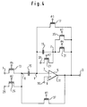
- Fig.4 is a circuit diagram of a gain stage according to the invention.
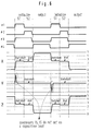
- Fig.5 is a timing diagram relating to the gain stage shown in figure 4.
- Fig.6 is a timing diagram relating to the gain stage shown in figure 4.
- Fig.7 is a circuit diagram of a gain stage according to the invention.
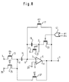
- Fig.8 is a circuit diagram of a gain stage according to the invention.
- Fig.9 is a circuit diagram of a gain stage according to the invention.
- Fig.10 is a circuit diagram of a CMOS switch.
- FIG. 4 shows a gain stage according to a first embodiment of this invention.
- an input terminal 1 is coupled to one node X of a condensor 15 through an MOS switch 13, and a reference input terminal 29 is also coupled to the node X through an MOS switch 25.
- the other node Y of the condensor 15 is coupled to an inverting input node 7 of an OP-amp 5, and a reference input terminal 30 is coupled to a non-inverting input node 9 of the OP-amp 5.
- An output node 11 of the OP-amp 5 is coupled to an output terminal 3.
- the output node 11 of the OP-amp 5 is coupled to the inverting input node 7 of the OP-amp 5 through an MOS switch 17 and through the serial connection of an MOS switch 21 and a condensor 19.
- the output node 11 is coupled to the node Z through an MOS switch 35.
- a reference input terminal 31 is coupled to the node Z through an MOS switch 27.
- the output node 11 is also coupled to the node X through an MOS switch 37.
- Each of the MOS switches have a control gate, and control signal ⁇ 1 is input the control gates of the MOS switches 35,37, control signal ⁇ 2 is input the control gates of the MOS switches 25,27, control signal ⁇ 3 is input the control gate of the MOS switch 17, and control signal ⁇ 4 is input the control gates of the MOS switches 13,21.
- Control signals ⁇ 1, ⁇ 2, ⁇ 3, ⁇ 4 turn the MOS switches OFF during the period of "L” level, and ON during the period of "H” level.
- Figure 5 is a timing diagram showing the control signals ⁇ 1, ⁇ 2, ⁇ 3, ⁇ 4, and is divided into first and second initialize periods, and an output period.
- the control signals ⁇ 2, ⁇ 4 are at the "L" level, thus the MOS switches 13,21,25,27 are OFF.
- the control signals ⁇ 1, ⁇ 3 are at the "H” level, so the MOS switches 17,35,37 are ON.
- MOS switches 17 and 35 the nodes Y and Z (ends of condensor 19) are short-circuited, and as MOS switches 17 and 35 are ON, nodes X and Y (ends of condensor 15) become short-circuits. Accordingly the charge stored in both condensors 15,19 is discharged and the nodes X,Y,Z are at the same voltage level.
- the control signals ⁇ 1, ⁇ 4 are at the "L" level, thus the MOS switches 13,21,35,37 are OFF.
- the control signal ⁇ 3 is still at the "H” level, so the MOS switch 17 is ON.
- the control signal ⁇ 2 rises to the "H” level, so the MOS switches 25,27 turn ON.
- Nodes X,Z are charged to Vref through the MOS switches 25,27, and node Y remains at Vref + Voff since the MOS switch 17 is still ON.
- ⁇ 2, ⁇ 3 have dropped to the "L” level and the MOS switches 17,25,27 turn OFF.
- the control signals ⁇ 1, ⁇ 2, ⁇ 3 are at the "L" level and the MOS switches 17,25,27,35,37 are still OFF.
- the control signal ⁇ 4 has risen to the "H” level, so the MOS switches 13,21 turn ON. Vin is applied to node X through the MOS switch 13, and Vout is applied to node Z through the MOS switch 21.
- the node Y is in a High-Impedance-state.
- the gain stage outputs the voltage level which inverts the input voltage level about Vref and removes the characteristic offset voltage of the OP-amp.
- FIG. 6 is an example of a timing diagram relating to the gain stage in figure 4.
- the nodes X,Y,Z are charged to Vref + Voff by the output 11 of the OP-amp 5.
- the control signal ⁇ 1 rises to "H" level, then the nodes X,Y,Z are short-circuited through the MOS switches 17,35,37.
- the nodes X,Y,Z are charged toward the latest output level of the gain stage, and next the nodes X,Y,Z are charged to Vref + Voff by the output 11 of the OP-amp 5 which acts as one component of the voltage follower circuit.
- both of the condensors 15,19 do not act as a capacitive load for the OP-amp 5, because the electrodes of the condensors 15,19 are short-circuited. So the charging speed is almost equal to the speed determined by slew rate of the OP-amp 5.
- the node Y is still at Vref + Voff, and the nodes X,Z are charged to Vref. This charging is easy so that the transition level is only from Vref + Voff to Vref, the difference level Voff being always very small. In this way, according to this embodiment, the initialize period is shortened, and the electric current consumed can be restrained.
- FIG. 7 is the circuit diagram illustrating the configuration of a gain stage according to the second embodiment of this invention.
- This gain stage has the same configuration as shown in figure 5 except that the MOS switch 37 is replaced by MOS switch 39 controlled by ⁇ 1.
- MOS switch 39 is ON during a period from T0 to T1, shorting node X to the output 11 of the OP-amp 5 since the MOS switch 17 is also ON.
- FIG 8 is the circuit diagram illustrating the configuration of a gain stage according to a third embodiment of this invention.
- the MOS switch 35 and the MOS switch 21 shown in figure 4 have been replaced by an MOS switch 21 controlled by the output of an OR gate 41 whose inputs are control signals ⁇ 1, ⁇ 4. Because there are typically many gain stages in a device, eliminating one MOS switch according to this embodiment can reduce the device area since only one OR gate can drive many gain stages.
- FIG. 9 is the circuit diagram illustrating the configuration of a gain stage according to a fourth embodiment of this invention.
- the MOS switch 17 shown in figure 4 has been replaced by two MOS switches 17a,17b controlled by ⁇ 2, ⁇ 1 respectively. So there is no need for the control signal ⁇ 3.
- a MOS switch in the gain stages mentioned above embodiments may be replaced by a CMOS switch.
- the switch is generally comprised of a P-channel MOS transistor PT and a N-channel MOS transistor NT as shown in figure 10, the circuit diagram of a CMOS switch. Both of the drain/source of the transistors NT,PT are connected to each other, and a control signal is input through clock terminal CK to the gate of the N-channel MOS transistor NT, and an inverted control signal is input through inverted clock terminal CKN to the gate of the P-channel MOS transistor PT.
- CMOS switch is effective to eliminate the switching resistance.
Landscapes
- Engineering & Computer Science (AREA)
- Power Engineering (AREA)
- Amplifiers (AREA)
- Filters That Use Time-Delay Elements (AREA)
Applications Claiming Priority (3)
| Application Number | Priority Date | Filing Date | Title |
|---|---|---|---|
| JP27118295 | 1995-10-19 | ||
| JP271182/95 | 1995-10-19 | ||
| JP27118295 | 1995-10-19 |
Publications (3)
| Publication Number | Publication Date |
|---|---|
| EP0769848A2 true EP0769848A2 (fr) | 1997-04-23 |
| EP0769848A3 EP0769848A3 (fr) | 1999-07-14 |
| EP0769848B1 EP0769848B1 (fr) | 2003-10-29 |
Family
ID=17496497
Family Applications (1)
| Application Number | Title | Priority Date | Filing Date |
|---|---|---|---|
| EP96116683A Expired - Lifetime EP0769848B1 (fr) | 1995-10-19 | 1996-10-17 | Etage amplificateur et méthode pour éliminer la tension d'offset |
Country Status (5)
| Country | Link |
|---|---|
| US (1) | US5880630A (fr) |
| EP (1) | EP0769848B1 (fr) |
| KR (1) | KR100244798B1 (fr) |
| DE (1) | DE69630505T2 (fr) |
| TW (1) | TW328191B (fr) |
Families Citing this family (7)
| Publication number | Priority date | Publication date | Assignee | Title |
|---|---|---|---|---|
| US6049247A (en) * | 1997-12-16 | 2000-04-11 | Photobit Corporation | Low-voltage common source switched-capacitor amplifier |
| US6064004A (en) * | 1998-06-24 | 2000-05-16 | Rgr Technologies, Inc | Electrical wiring installation apparatus and method |
| US6091293A (en) * | 1999-03-26 | 2000-07-18 | National Semiconductor Corporation | Amplifier circuit having AC reset capability and method |
| US6140871A (en) * | 1999-03-26 | 2000-10-31 | National Semiconductor Corporation | Switched capacitor amplifier circuit having bus precharge capability and method |
| US6211729B1 (en) * | 1999-09-07 | 2001-04-03 | Agilent Technologies, Inc. | Amplifier circuit with a switch bypass |
| US7230479B2 (en) * | 2005-08-03 | 2007-06-12 | Micron Technology, Inc. | Technique to improve the gain and signal to noise ratio in CMOS switched capacitor amplifiers |
| JP6057602B2 (ja) * | 2012-08-10 | 2017-01-11 | キヤノン株式会社 | 固体撮像装置 |
Citations (1)
| Publication number | Priority date | Publication date | Assignee | Title |
|---|---|---|---|---|
| US4404525A (en) | 1981-03-03 | 1983-09-13 | American Microsystems, Inc. | Switched capacitor gain stage with offset and switch feedthrough cancellation scheme |
Family Cites Families (5)
| Publication number | Priority date | Publication date | Assignee | Title |
|---|---|---|---|---|
| US4393351A (en) * | 1981-07-27 | 1983-07-12 | American Microsystems, Inc. | Offset compensation for switched capacitor integrators |
| US4529965A (en) * | 1983-05-03 | 1985-07-16 | Racal Data Communications | Switched-capacitor circuit analog-to-digital converter |
| US4565971A (en) * | 1985-01-28 | 1986-01-21 | Motorola, Inc. | Parasitic insensitive auto-zeroed operational amplifier |
| NL9200327A (nl) * | 1992-02-21 | 1993-09-16 | Sierra Semiconductor Bv | Offset-gecompenseerde bemonsterinrichting en werkwijze voor de bediening daarvan. |
| US5479130A (en) * | 1994-02-15 | 1995-12-26 | Analog Devices, Inc. | Auto-zero switched-capacitor integrator |
-
1996
- 1996-10-10 US US08/729,294 patent/US5880630A/en not_active Expired - Fee Related
- 1996-10-11 TW TW085112436A patent/TW328191B/zh not_active IP Right Cessation
- 1996-10-17 KR KR1019960046420A patent/KR100244798B1/ko not_active Expired - Fee Related
- 1996-10-17 DE DE69630505T patent/DE69630505T2/de not_active Expired - Lifetime
- 1996-10-17 EP EP96116683A patent/EP0769848B1/fr not_active Expired - Lifetime
Patent Citations (1)
| Publication number | Priority date | Publication date | Assignee | Title |
|---|---|---|---|---|
| US4404525A (en) | 1981-03-03 | 1983-09-13 | American Microsystems, Inc. | Switched capacitor gain stage with offset and switch feedthrough cancellation scheme |
Also Published As
| Publication number | Publication date |
|---|---|
| US5880630A (en) | 1999-03-09 |
| KR100244798B1 (ko) | 2000-02-15 |
| DE69630505T2 (de) | 2004-08-05 |
| EP0769848B1 (fr) | 2003-10-29 |
| TW328191B (en) | 1998-03-11 |
| DE69630505D1 (de) | 2003-12-04 |
| EP0769848A3 (fr) | 1999-07-14 |
| KR970024530A (ko) | 1997-05-30 |
Similar Documents
| Publication | Publication Date | Title |
|---|---|---|
| US20070159233A1 (en) | Charge pump power supply circuit | |
| EP0086090B1 (fr) | Circuit d'attaque pour charges capacitives | |
| JPH0897700A (ja) | 出力バッファ回路 | |
| US10476383B2 (en) | Negative charge pump circuit | |
| CN1018489B (zh) | 互补金属氧化物半导体存储器驱动器电路 | |
| JPH0322728B2 (fr) | ||
| US5552747A (en) | Driver circuit compatible with low supply voltages | |
| US4550295A (en) | Switched capacitor integrator | |
| EP0769848B1 (fr) | Etage amplificateur et méthode pour éliminer la tension d'offset | |
| US6982577B2 (en) | Power-on reset circuit | |
| JP2968826B2 (ja) | カレントミラー型増幅回路及びその駆動方法 | |
| JPH02119427A (ja) | 出力バッファ回路 | |
| US6806760B2 (en) | Low-voltage booster circuits and methods of operation thereof | |
| US4611134A (en) | Bootstrap driving circuit | |
| EP0868026A1 (fr) | Circuit à retard variable | |
| JP2871902B2 (ja) | 電流セル回路 | |
| JPH01161913A (ja) | クロックドライバー回路 | |
| JP3047828B2 (ja) | コンパレータ回路 | |
| KR100299050B1 (ko) | 상보 게이트-소스 클럭구동회로와 이를 적용한 플립플롭 | |
| JP4530503B2 (ja) | インピーダンス変換回路 | |
| EP0768759A2 (fr) | Circuit de retard analogique | |
| KR960015319B1 (ko) | 반도체 메모리 장치의 전압 변환회로 | |
| KR930006747Y1 (ko) | 모스용 승압회로 | |
| JPS6347010B2 (fr) | ||
| JPH0235821A (ja) | 論理回路 |
Legal Events
| Date | Code | Title | Description |
|---|---|---|---|
| PUAI | Public reference made under article 153(3) epc to a published international application that has entered the european phase |
Free format text: ORIGINAL CODE: 0009012 |
|
| 17P | Request for examination filed |
Effective date: 19961017 |
|
| AK | Designated contracting states |
Kind code of ref document: A2 Designated state(s): DE FR GB |
|
| PUAL | Search report despatched |
Free format text: ORIGINAL CODE: 0009013 |
|
| AK | Designated contracting states |
Kind code of ref document: A3 Designated state(s): DE FR GB |
|
| RTI1 | Title (correction) |
Free format text: A GAIN STAGE AND OFFSET VOLTAGE ELIMINATION METHOD |
|
| 17Q | First examination report despatched |
Effective date: 20020729 |
|
| GRAH | Despatch of communication of intention to grant a patent |
Free format text: ORIGINAL CODE: EPIDOS IGRA |
|
| GRAS | Grant fee paid |
Free format text: ORIGINAL CODE: EPIDOSNIGR3 |
|
| GRAA | (expected) grant |
Free format text: ORIGINAL CODE: 0009210 |
|
| AK | Designated contracting states |
Kind code of ref document: B1 Designated state(s): DE FR GB |
|
| REG | Reference to a national code |
Ref country code: GB Ref legal event code: FG4D |
|
| REF | Corresponds to: |
Ref document number: 69630505 Country of ref document: DE Date of ref document: 20031204 Kind code of ref document: P |
|
| ET | Fr: translation filed | ||
| PLBE | No opposition filed within time limit |
Free format text: ORIGINAL CODE: 0009261 |
|
| STAA | Information on the status of an ep patent application or granted ep patent |
Free format text: STATUS: NO OPPOSITION FILED WITHIN TIME LIMIT |
|
| 26N | No opposition filed |
Effective date: 20040730 |
|
| PGFP | Annual fee paid to national office [announced via postgrant information from national office to epo] |
Ref country code: DE Payment date: 20091015 Year of fee payment: 14 |
|
| PGFP | Annual fee paid to national office [announced via postgrant information from national office to epo] |
Ref country code: GB Payment date: 20091014 Year of fee payment: 14 Ref country code: FR Payment date: 20091029 Year of fee payment: 14 |
|
| GBPC | Gb: european patent ceased through non-payment of renewal fee |
Effective date: 20101017 |
|
| PG25 | Lapsed in a contracting state [announced via postgrant information from national office to epo] |
Ref country code: FR Free format text: LAPSE BECAUSE OF NON-PAYMENT OF DUE FEES Effective date: 20101102 |
|
| REG | Reference to a national code |
Ref country code: FR Ref legal event code: ST Effective date: 20110630 |
|
| REG | Reference to a national code |
Ref country code: DE Ref legal event code: R119 Ref document number: 69630505 Country of ref document: DE Effective date: 20110502 |
|
| PG25 | Lapsed in a contracting state [announced via postgrant information from national office to epo] |
Ref country code: GB Free format text: LAPSE BECAUSE OF NON-PAYMENT OF DUE FEES Effective date: 20101017 |
|
| PG25 | Lapsed in a contracting state [announced via postgrant information from national office to epo] |
Ref country code: DE Free format text: LAPSE BECAUSE OF NON-PAYMENT OF DUE FEES Effective date: 20110502 |