EP0770201B1 - Procede permettant de mesurer la profondeur d'une microstructure - Google Patents
Procede permettant de mesurer la profondeur d'une microstructure Download PDFInfo
- Publication number
- EP0770201B1 EP0770201B1 EP95921698A EP95921698A EP0770201B1 EP 0770201 B1 EP0770201 B1 EP 0770201B1 EP 95921698 A EP95921698 A EP 95921698A EP 95921698 A EP95921698 A EP 95921698A EP 0770201 B1 EP0770201 B1 EP 0770201B1
- Authority
- EP
- European Patent Office
- Prior art keywords
- depth
- measuring
- light beam
- embossing
- light
- Prior art date
- Legal status (The legal status is an assumption and is not a legal conclusion. Google has not performed a legal analysis and makes no representation as to the accuracy of the status listed.)
- Expired - Lifetime
Links
- 238000000034 method Methods 0.000 title claims abstract description 29
- 238000004049 embossing Methods 0.000 claims description 22
- 230000005540 biological transmission Effects 0.000 claims description 14
- 238000001228 spectrum Methods 0.000 claims description 6
- 230000000052 comparative effect Effects 0.000 claims description 3
- 238000011156 evaluation Methods 0.000 claims description 3
- 230000001419 dependent effect Effects 0.000 claims description 2
- 238000000926 separation method Methods 0.000 claims 1
- 238000009826 distribution Methods 0.000 abstract description 9
- 238000005259 measurement Methods 0.000 description 25
- 239000000758 substrate Substances 0.000 description 18
- 230000000694 effects Effects 0.000 description 4
- 230000003595 spectral effect Effects 0.000 description 4
- 239000003086 colorant Substances 0.000 description 3
- 230000000149 penetrating effect Effects 0.000 description 3
- 230000005855 radiation Effects 0.000 description 3
- 230000000007 visual effect Effects 0.000 description 3
- 230000002349 favourable effect Effects 0.000 description 2
- 238000004519 manufacturing process Methods 0.000 description 2
- 239000002184 metal Substances 0.000 description 2
- 238000002834 transmittance Methods 0.000 description 2
- 241001465754 Metazoa Species 0.000 description 1
- 230000002411 adverse Effects 0.000 description 1
- 230000009286 beneficial effect Effects 0.000 description 1
- 230000015572 biosynthetic process Effects 0.000 description 1
- 239000011248 coating agent Substances 0.000 description 1
- 238000000576 coating method Methods 0.000 description 1
- 238000012937 correction Methods 0.000 description 1
- 230000003247 decreasing effect Effects 0.000 description 1
- 230000009365 direct transmission Effects 0.000 description 1
- 239000011888 foil Substances 0.000 description 1
- 238000000691 measurement method Methods 0.000 description 1
- 238000005457 optimization Methods 0.000 description 1
- 230000000737 periodic effect Effects 0.000 description 1
- 238000002360 preparation method Methods 0.000 description 1
- 238000012549 training Methods 0.000 description 1
- 239000012780 transparent material Substances 0.000 description 1
Images

Classifications
-
- G—PHYSICS
- G01—MEASURING; TESTING
- G01B—MEASURING LENGTH, THICKNESS OR SIMILAR LINEAR DIMENSIONS; MEASURING ANGLES; MEASURING AREAS; MEASURING IRREGULARITIES OF SURFACES OR CONTOURS
- G01B11/00—Measuring arrangements characterised by the use of optical techniques
- G01B11/22—Measuring arrangements characterised by the use of optical techniques for measuring depth
Definitions
- the invention relates to a method for measuring the depth a microstructure when transferring the structure by means of an embossing process in a deformable layer.
- Diffractive optically effective structures which means a so-called "master” into a corresponding one deformable layer are embossed.
- stamping foils are produced in this way, by which then the security element in a hot stamping process is transferred to a substrate.
- embossing depths in the Order of magnitude of sometimes less than 1 ⁇ m, on the one hand the embossing must not be too shallow, otherwise the desired effect not with the required Clarity occurs.
- the invention is therefore based on the object Method of measuring the depth of a microstructure propose which is particularly simple, universal applied and also with comparative low cost can be realized.
- the basic principle of the method according to the invention lies thus in that for measuring the embossing depth of the Microstructure at least in a certain area
- Reference structure is introduced, which is a geometrically simple lattice structure, preferably with a square, rectangular or triangular profile acts.
- the spectral distribution of the passing or reflected light measured, the occurring Intensity maxima or minima as a direct measure of the Embossing depth can be used because these maxima or Minima differ depending on the embossing depth Wander wavelengths of the color spectrum. It is in the general so that the minimum wavelength with Reduction in structure depth migrates to smaller values.
- the absolute value of the minimum frequency depends on correct selected reference grid profile essentially from Refractive index of the substrate to be structured.
- the method according to the invention the following considerations, on the one hand Measurement in transmission and on the other hand in reflection to be examined.
- T ( ⁇ ) cos 2nd [ ⁇ 2nd ⁇ (A + c 1 ) ⁇ n-1 ⁇ + c 2nd ]
- a reflective structure is to be measured, it is more advantageous if light is used as the measuring light beam a limited wavelength range is used. In this case it is possible to use white light occurring maximum and minimum intensity switch off different frequencies for the most part, so that then for the actual structure depth measurement clear allocation between intensity minimum and Structure depth is present.
- the subject relates to the present Invention a method for measuring the embossing depth Microstructure during the embossing process, during which Assessment of the embossed microstructure at least in one specific area of the microstructure a reference structure is introduced, this reference structure with a Light beam of a certain wavelength range is irradiated and the occurring intensity maxima or minima in Diffraction spectrum of the 0th order as a direct measure of the embossing depth reached or approximated Color of light is assessed visually.
- Figures 1a - 1c it is illustrated that as Reference lattice structure for the method according to the Invention simple structures used as possible should be, the grid structure according to Figure la around a so-called rectangular grid, in which Grid structure according to Figure 1b around a square grid and in the structure according to FIG. 1c by a triangular one Grid acts.
- the lattice structures of Figures 1a to 1c are generated simultaneously with the generation of the other Microstructure formed in a substrate, one Corresponding embossing of the substrate 1 takes place, whereby Lattice webs 2 and spaces 3 between the lattice webs arise.
- la to lc are different geometric shape, but also in the other different purpose.
- the lattice structures according to Figures la and lc are namely for use with Transmission measurement thought during the lattice structure 1b can be used for reflection measurement.
- the lattice structures should meet the following conditions: Lattice constant g 0.5 ⁇ m ⁇ g ⁇ 4 ⁇ m Web / lattice constant ratio b / g 0.1 ⁇ b / g ⁇ 0.8 Grid depth a 0.3 ⁇ m ⁇ a ⁇ 4 ⁇ m.
- Figure 2 is the measurement method for measuring the Structure depth in a transparent substrate 5 illustrated.
- the substrate 5 at least in some areas with a corresponding reference lattice structure provided, in which shown Embodiment the grid structure is a square Lattice structure, i.e. in cross section of the lattice structure corresponds to Figure 1b, but without reflective Education.
- This reference lattice structure is created using a Light source 6, which is directed accordingly with Illuminated white light and then the spectral color distribution of the substrate 5 or the reference lattice structure penetrating light 7 by means of a receiver 8, expediently measured by a spectrophotometer.
- the intensity distribution T ( ⁇ ) of the light falling on the receiver 8 as a function of the wavelength ⁇ is shown in principle in FIG. 4, with a minimum of the radiation intensity T ( ⁇ ) depending on the depth a of the reference grating structure of the substrate 5 during transmission measurement. at a certain wavelength min .
- the structure depth a obtained in each case can thus be determined in a simple and rapid manner simply by determining the wavelength of the intensity minimum.
- the measuring arrangement for the determination of the structure depth at a reflective substrate is shown schematically in FIG. 3 shown.
- the substrate 5 ' is also with a reference lattice structure the structure depth a.
- the formation such that at least the light source 6 ' and the receiver 8 ', which is on the same side of the Substrate 5 'as the light source 6' is arranged, indicative surface of the substrate 5 'reflective, e.g. is provided with a metallic coating 9.
- light source 6 'and receiver 8' can be used the light source 6 or the receiver 8 of the arrangement for Transmission measurement match. However, it can Reflection measurement be more favorable if the light source 6 ' only emits light of a limited wavelength range or the receiver 8 'light of a particular one Wavelength range because then a direct one Assignment of intensity minima and maxima of the Receiver 8 'incident, reflected light from the Light source 6 'possible to a certain structure depth a is.
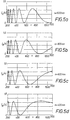
- FIGS. 5a to 5d show the intensity distribution I R of the light reflected by the reflecting surface 9 of the substrate 5 'as a function of the wavelength, with FIGS. 5a to 5d showing the intensity distribution when reflected at an air-metal boundary layer and using white light.
- the intensity distribution corresponds essentially to the above formula (III), the constant c being assumed to be -50 nm.
Landscapes
- Physics & Mathematics (AREA)
- General Physics & Mathematics (AREA)
- Length Measuring Devices By Optical Means (AREA)
- Investigating Or Analysing Materials By Optical Means (AREA)
- Analysing Materials By The Use Of Radiation (AREA)
Claims (7)
- Procédé de mesure de la profondeur d'une microstructure lors du transfert de la structure dans une couche déformable au moyen d'un procédé d'impression,
caractériséen ce que, dans la microstructure à transférer, il est prévu, au moins par endroits, une structure de réseau de référence géométriquement simple,en ce que la structure de réseau de référence reçoit un rayon de lumière qui présente une plage déterminée de longueurs d'onde,en ce que la longueur d'onde, qui dépend de la profondeur d'impression obtenue, des maxima d'intensité ou minima d'intensité se présentant dans le spectre de diffraction d'ordre 0 est mesurée en transmission ou en réflexion et, sur la base de valeurs de comparaison prévues pour la structure de référence chaque fois considérée et la plage de longueurs d'onde rayonnées, la profondeur d'impression obtenue est déterminée à partir de la longueur d'onde mesuréeou en ce qu'à partir de l'évaluation intégrale de la couleur de la lumière diffractée d'ordre 0, la profondeur d'impression obtenue est déduite sur la base de valeurs de comparaison. - Procédé suivant la revendication 1, caractérisé en ce que la structure de réseau de référence présente une forme profilée carrée, rectangulaire ou triangulaire.
- Procédé suivant la revendication 1 ou 2, caractérisé en ce que la structure de réseau de référence présente les paramètres suivants :
constante de réseau g 0,5 µm £ g < 4 µm rapport relief/constante de réseau b/g 0,1 £ b/g £ 0,8 profondeur de réseau a 0,3 µm £ a £ 4 µm - Procédé suivant l'une des revendications précédentes, caractérisé en ce que l'analyse de couleur du rayon lumineux de mesure a lieu au moyen d'un spectrophotomètre.
- Procédé suivant l'une des revendications précédentes, caractérisé en ce que le rayon lumineux de mesure est formé d'une lumière visible.
- Procédé suivant la revendication 5, caractérisé en ce que de la lumière blanche est utilisée lors de l'analyse de la couleur du rayon lumineux de mesure traversant la structure de réseau de référence.
- Procédé suivant l'une des revendications 1 à 4, caractérisé en ce qu'une lumière présentant une plage limitée de longueurs d'onde est utilisée comme rayon lumineux de mesure.
Applications Claiming Priority (3)
| Application Number | Priority Date | Filing Date | Title |
|---|---|---|---|
| DE4424565 | 1994-07-13 | ||
| DE4424565A DE4424565C1 (de) | 1994-07-13 | 1994-07-13 | Verfahren zur Messung der Tiefe einer Mikrostruktur |
| PCT/DE1995/000783 WO1996002807A1 (fr) | 1994-07-13 | 1995-06-10 | Procede permettant de mesurer la profondeur d'une microstructure |
Publications (2)
| Publication Number | Publication Date |
|---|---|
| EP0770201A1 EP0770201A1 (fr) | 1997-05-02 |
| EP0770201B1 true EP0770201B1 (fr) | 1999-02-03 |
Family
ID=6522947
Family Applications (1)
| Application Number | Title | Priority Date | Filing Date |
|---|---|---|---|
| EP95921698A Expired - Lifetime EP0770201B1 (fr) | 1994-07-13 | 1995-06-10 | Procede permettant de mesurer la profondeur d'une microstructure |
Country Status (10)
| Country | Link |
|---|---|
| EP (1) | EP0770201B1 (fr) |
| JP (1) | JPH10502734A (fr) |
| AT (1) | ATE176526T1 (fr) |
| AU (1) | AU691622B2 (fr) |
| BR (1) | BR9508275A (fr) |
| CA (1) | CA2194883A1 (fr) |
| DE (2) | DE4424565C1 (fr) |
| ES (1) | ES2127535T3 (fr) |
| TW (1) | TW251346B (fr) |
| WO (1) | WO1996002807A1 (fr) |
Families Citing this family (4)
| Publication number | Priority date | Publication date | Assignee | Title |
|---|---|---|---|---|
| DE19632763C2 (de) * | 1996-08-14 | 1998-09-10 | Holger Moritz | Meßkopf für die Beobachtung der Photolackentwicklung |
| DE19652563A1 (de) * | 1996-12-17 | 1998-06-18 | Heidenhain Gmbh Dr Johannes | Lichtelektrische Positionsmeßeinrichtung |
| DE19702851C1 (de) * | 1997-01-27 | 1998-08-06 | Deutsch Zentr Luft & Raumfahrt | Verfahren und Vorrichtung zur Prüfung offener, aber nicht vollständig einsehbarer Hohlräume |
| DE19739885A1 (de) * | 1997-09-11 | 1999-03-18 | Bernd Klose | Komparativer Oberflächenqualifizierer |
Family Cites Families (5)
| Publication number | Priority date | Publication date | Assignee | Title |
|---|---|---|---|---|
| DE3518774A1 (de) * | 1985-05-24 | 1986-11-27 | Dr. Johannes Heidenhain Gmbh, 8225 Traunreut | Verfahren zur ermittlung und optimierung der optischen weglaenge einer durchgehenden transparenten schicht oder einer strukturierten schicht |
| JPH0617774B2 (ja) * | 1987-06-22 | 1994-03-09 | 大日本スクリ−ン製造株式会社 | 微小高低差測定装置 |
| JPH0223617A (ja) * | 1988-07-13 | 1990-01-25 | Mitsubishi Electric Corp | 半導体基板ウェハの溝形成方法 |
| FR2665024B1 (fr) * | 1990-07-20 | 1994-02-18 | Jean Galvier | Procede de determination de l'elimination complete d'une couche mince sur un substrat non plan. |
| US5361137A (en) * | 1992-08-31 | 1994-11-01 | Texas Instruments Incorporated | Process control for submicron linewidth measurement |
-
1994
- 1994-07-13 DE DE4424565A patent/DE4424565C1/de not_active Expired - Fee Related
- 1994-09-07 TW TW083108245A patent/TW251346B/zh active
-
1995
- 1995-06-10 EP EP95921698A patent/EP0770201B1/fr not_active Expired - Lifetime
- 1995-06-10 DE DE59505046T patent/DE59505046D1/de not_active Expired - Fee Related
- 1995-06-10 ES ES95921698T patent/ES2127535T3/es not_active Expired - Lifetime
- 1995-06-10 BR BR9508275A patent/BR9508275A/pt not_active Application Discontinuation
- 1995-06-10 WO PCT/DE1995/000783 patent/WO1996002807A1/fr not_active Ceased
- 1995-06-10 AU AU26682/95A patent/AU691622B2/en not_active Ceased
- 1995-06-10 CA CA002194883A patent/CA2194883A1/fr not_active Abandoned
- 1995-06-10 AT AT95921698T patent/ATE176526T1/de not_active IP Right Cessation
- 1995-06-10 JP JP8504567A patent/JPH10502734A/ja active Pending
Also Published As
| Publication number | Publication date |
|---|---|
| CA2194883A1 (fr) | 1996-02-01 |
| DE4424565C1 (de) | 1995-08-24 |
| AU691622B2 (en) | 1998-05-21 |
| DE59505046D1 (de) | 1999-03-18 |
| ATE176526T1 (de) | 1999-02-15 |
| EP0770201A1 (fr) | 1997-05-02 |
| BR9508275A (pt) | 1997-11-04 |
| ES2127535T3 (es) | 1999-04-16 |
| TW251346B (en) | 1995-07-11 |
| JPH10502734A (ja) | 1998-03-10 |
| WO1996002807A1 (fr) | 1996-02-01 |
| AU2668295A (en) | 1996-02-16 |
Similar Documents
| Publication | Publication Date | Title |
|---|---|---|
| EP1458578B1 (fr) | Element de securite a diffraction | |
| DE3751924T2 (de) | Verfahren und Vorrichtung zum Nachweisen oder zur Bestimmung einer oder mehrerer Eigenschaften oder zum Identifizieren einer Probe | |
| DE3248899C2 (fr) | ||
| EP3331709B1 (fr) | Élément de sécurité muni d'un réseau sub-longueur d'onde | |
| CH661602A5 (de) | Kennzeichnungsvorrichtung fuer einen blattfoermigen gegenstand. | |
| DE102014010751A1 (de) | Sicherheitselement mit Subwellenlängengitter | |
| DE69327146T2 (de) | Prozesssteuerung zur Submikronlinienbreitenmessung | |
| EP2874820B1 (fr) | Élément de sécurité pour papiers de sécurité, documents fiduciaires ou similaires | |
| DE3322639C2 (de) | Konkavgitterspektrometer | |
| DE3851370T2 (de) | Testvorrichtung zur Durchführung eines Realisierungsverfahrens von Halbleiterstrukturen. | |
| EP0770201B1 (fr) | Procede permettant de mesurer la profondeur d'une microstructure | |
| DE2748064C3 (de) | Subtraktives Farbfiltersystem mit einem Phasengitter | |
| DE102017009226A1 (de) | Optisch variables Durchsichtssicherheitselement und Datenträger | |
| EP0883899B1 (fr) | Procede pour determiner l'orientation de cristaux dans une plaquette | |
| DE3721749A1 (de) | Verfahren und vorrichtung zur beruehrungslosen erfassung der form von gegenstaenden | |
| EP1012838A1 (fr) | Procede de regulation d'un processus d'application de revetement | |
| EP3060887B1 (fr) | Échelle de mesure pour capteur incrémentiel et son procédé de fabrication | |
| DE102007003824B4 (de) | Verfahren zum Auftragen einer Wärmeleitpaste | |
| DE69314640T2 (de) | Verfahren zum Erhalten von zwei Druckbildern auf harten Oberflächen | |
| EP3541630B1 (fr) | Élément de sécurité muni d'un réseau sub-longueur d'onde | |
| EP0506675A1 (fr) | Procede pour la determination de la position d'une jonction pn. | |
| DE10227376B4 (de) | Verfahren zur Bestimmung von Schichtdickenbereichen | |
| DE69917110T2 (de) | Glasscheibe | |
| EP3898248B1 (fr) | Élément de sécurité actif dans le domaine des thz et son procédé de fabrication | |
| DE19838611B4 (de) | Farbenmesser |
Legal Events
| Date | Code | Title | Description |
|---|---|---|---|
| PUAI | Public reference made under article 153(3) epc to a published international application that has entered the european phase |
Free format text: ORIGINAL CODE: 0009012 |
|
| 17P | Request for examination filed |
Effective date: 19970121 |
|
| AK | Designated contracting states |
Kind code of ref document: A1 Designated state(s): AT BE CH DE DK ES FR GB IT LI LU NL PT SE |
|
| GRAG | Despatch of communication of intention to grant |
Free format text: ORIGINAL CODE: EPIDOS AGRA |
|
| 17Q | First examination report despatched |
Effective date: 19980507 |
|
| GRAG | Despatch of communication of intention to grant |
Free format text: ORIGINAL CODE: EPIDOS AGRA |
|
| GRAH | Despatch of communication of intention to grant a patent |
Free format text: ORIGINAL CODE: EPIDOS IGRA |
|
| GRAH | Despatch of communication of intention to grant a patent |
Free format text: ORIGINAL CODE: EPIDOS IGRA |
|
| GRAA | (expected) grant |
Free format text: ORIGINAL CODE: 0009210 |
|
| AK | Designated contracting states |
Kind code of ref document: B1 Designated state(s): AT BE CH DE DK ES FR GB IT LI LU NL PT SE |
|
| REF | Corresponds to: |
Ref document number: 176526 Country of ref document: AT Date of ref document: 19990215 Kind code of ref document: T |
|
| REG | Reference to a national code |
Ref country code: CH Ref legal event code: EP |
|
| REG | Reference to a national code |
Ref country code: CH Ref legal event code: NV Representative=s name: FIAMMENGHI-FIAMMENGHI |
|
| GBT | Gb: translation of ep patent filed (gb section 77(6)(a)/1977) |
Effective date: 19990219 |
|
| REF | Corresponds to: |
Ref document number: 59505046 Country of ref document: DE Date of ref document: 19990318 |
|
| ET | Fr: translation filed | ||
| REG | Reference to a national code |
Ref country code: ES Ref legal event code: FG2A Ref document number: 2127535 Country of ref document: ES Kind code of ref document: T3 |
|
| ITF | It: translation for a ep patent filed | ||
| PG25 | Lapsed in a contracting state [announced via postgrant information from national office to epo] |
Ref country code: PT Free format text: LAPSE BECAUSE OF FAILURE TO SUBMIT A TRANSLATION OF THE DESCRIPTION OR TO PAY THE FEE WITHIN THE PRESCRIBED TIME-LIMIT Effective date: 19990503 Ref country code: DK Free format text: LAPSE BECAUSE OF FAILURE TO SUBMIT A TRANSLATION OF THE DESCRIPTION OR TO PAY THE FEE WITHIN THE PRESCRIBED TIME-LIMIT Effective date: 19990503 |
|
| PG25 | Lapsed in a contracting state [announced via postgrant information from national office to epo] |
Ref country code: LU Free format text: LAPSE BECAUSE OF NON-PAYMENT OF DUE FEES Effective date: 19990610 |
|
| PLBE | No opposition filed within time limit |
Free format text: ORIGINAL CODE: 0009261 |
|
| STAA | Information on the status of an ep patent application or granted ep patent |
Free format text: STATUS: NO OPPOSITION FILED WITHIN TIME LIMIT |
|
| 26N | No opposition filed | ||
| REG | Reference to a national code |
Ref country code: GB Ref legal event code: IF02 |
|
| PGFP | Annual fee paid to national office [announced via postgrant information from national office to epo] |
Ref country code: BE Payment date: 20020620 Year of fee payment: 8 Ref country code: AT Payment date: 20020620 Year of fee payment: 8 |
|
| PGFP | Annual fee paid to national office [announced via postgrant information from national office to epo] |
Ref country code: SE Payment date: 20020624 Year of fee payment: 8 |
|
| PGFP | Annual fee paid to national office [announced via postgrant information from national office to epo] |
Ref country code: ES Payment date: 20020625 Year of fee payment: 8 |
|
| PG25 | Lapsed in a contracting state [announced via postgrant information from national office to epo] |
Ref country code: AT Free format text: LAPSE BECAUSE OF NON-PAYMENT OF DUE FEES Effective date: 20030610 |
|
| PG25 | Lapsed in a contracting state [announced via postgrant information from national office to epo] |
Ref country code: SE Free format text: LAPSE BECAUSE OF NON-PAYMENT OF DUE FEES Effective date: 20030611 Ref country code: ES Free format text: LAPSE BECAUSE OF NON-PAYMENT OF DUE FEES Effective date: 20030611 |
|
| PG25 | Lapsed in a contracting state [announced via postgrant information from national office to epo] |
Ref country code: BE Free format text: LAPSE BECAUSE OF NON-PAYMENT OF DUE FEES Effective date: 20030630 |
|
| BERE | Be: lapsed |
Owner name: LEONHARD *KURZ G.M.B.H. & CO. Effective date: 20030630 |
|
| EUG | Se: european patent has lapsed | ||
| REG | Reference to a national code |
Ref country code: ES Ref legal event code: FD2A Effective date: 20030611 |
|
| PG25 | Lapsed in a contracting state [announced via postgrant information from national office to epo] |
Ref country code: IT Free format text: LAPSE BECAUSE OF NON-PAYMENT OF DUE FEES;WARNING: LAPSES OF ITALIAN PATENTS WITH EFFECTIVE DATE BEFORE 2007 MAY HAVE OCCURRED AT ANY TIME BEFORE 2007. THE CORRECT EFFECTIVE DATE MAY BE DIFFERENT FROM THE ONE RECORDED. Effective date: 20050610 |
|
| PGFP | Annual fee paid to national office [announced via postgrant information from national office to epo] |
Ref country code: DE Payment date: 20060321 Year of fee payment: 12 |
|
| PGFP | Annual fee paid to national office [announced via postgrant information from national office to epo] |
Ref country code: NL Payment date: 20060619 Year of fee payment: 12 |
|
| PGFP | Annual fee paid to national office [announced via postgrant information from national office to epo] |
Ref country code: FR Payment date: 20060621 Year of fee payment: 12 |
|
| PGFP | Annual fee paid to national office [announced via postgrant information from national office to epo] |
Ref country code: GB Payment date: 20060626 Year of fee payment: 12 |
|
| PGFP | Annual fee paid to national office [announced via postgrant information from national office to epo] |
Ref country code: CH Payment date: 20060627 Year of fee payment: 12 |
|
| REG | Reference to a national code |
Ref country code: CH Ref legal event code: PL |
|
| GBPC | Gb: european patent ceased through non-payment of renewal fee |
Effective date: 20070610 |
|
| NLV4 | Nl: lapsed or anulled due to non-payment of the annual fee |
Effective date: 20080101 |
|
| REG | Reference to a national code |
Ref country code: FR Ref legal event code: ST Effective date: 20080229 |
|
| PG25 | Lapsed in a contracting state [announced via postgrant information from national office to epo] |
Ref country code: NL Free format text: LAPSE BECAUSE OF NON-PAYMENT OF DUE FEES Effective date: 20080101 Ref country code: LI Free format text: LAPSE BECAUSE OF NON-PAYMENT OF DUE FEES Effective date: 20070630 Ref country code: DE Free format text: LAPSE BECAUSE OF NON-PAYMENT OF DUE FEES Effective date: 20080101 Ref country code: CH Free format text: LAPSE BECAUSE OF NON-PAYMENT OF DUE FEES Effective date: 20070630 |
|
| PG25 | Lapsed in a contracting state [announced via postgrant information from national office to epo] |
Ref country code: GB Free format text: LAPSE BECAUSE OF NON-PAYMENT OF DUE FEES Effective date: 20070610 |
|
| PG25 | Lapsed in a contracting state [announced via postgrant information from national office to epo] |
Ref country code: FR Free format text: LAPSE BECAUSE OF NON-PAYMENT OF DUE FEES Effective date: 20070702 |