EP0770933A2 - Appareil de formation d'images - Google Patents
Appareil de formation d'images Download PDFInfo
- Publication number
- EP0770933A2 EP0770933A2 EP96117174A EP96117174A EP0770933A2 EP 0770933 A2 EP0770933 A2 EP 0770933A2 EP 96117174 A EP96117174 A EP 96117174A EP 96117174 A EP96117174 A EP 96117174A EP 0770933 A2 EP0770933 A2 EP 0770933A2
- Authority
- EP
- European Patent Office
- Prior art keywords
- film
- transfer
- transfer medium
- forming apparatus
- image forming
- Prior art date
- Legal status (The legal status is an assumption and is not a legal conclusion. Google has not performed a legal analysis and makes no representation as to the accuracy of the status listed.)
- Granted
Links
- 230000000274 adsorptive effect Effects 0.000 claims abstract description 27
- 238000011144 upstream manufacturing Methods 0.000 claims abstract description 23
- 238000006073 displacement reaction Methods 0.000 claims abstract description 10
- 239000010410 layer Substances 0.000 claims description 55
- 239000002344 surface layer Substances 0.000 claims description 11
- 239000000853 adhesive Substances 0.000 claims description 4
- 230000001070 adhesive effect Effects 0.000 claims description 4
- 239000002356 single layer Substances 0.000 claims description 3
- 239000010408 film Substances 0.000 description 140
- 238000010276 construction Methods 0.000 description 26
- 239000000126 substance Substances 0.000 description 24
- 229920005989 resin Polymers 0.000 description 22
- 239000011347 resin Substances 0.000 description 22
- 230000000694 effects Effects 0.000 description 15
- 229920001971 elastomer Polymers 0.000 description 8
- 230000005684 electric field Effects 0.000 description 6
- 239000000843 powder Substances 0.000 description 6
- 239000005060 rubber Substances 0.000 description 6
- 239000004677 Nylon Substances 0.000 description 5
- 229910052751 metal Inorganic materials 0.000 description 5
- 239000002184 metal Substances 0.000 description 5
- 229920001778 nylon Polymers 0.000 description 5
- PXHVJJICTQNCMI-UHFFFAOYSA-N Nickel Chemical compound [Ni] PXHVJJICTQNCMI-UHFFFAOYSA-N 0.000 description 4
- 239000004020 conductor Substances 0.000 description 4
- 230000014759 maintenance of location Effects 0.000 description 4
- 238000000034 method Methods 0.000 description 4
- 239000000203 mixture Substances 0.000 description 4
- 238000010186 staining Methods 0.000 description 4
- 229920002554 vinyl polymer Polymers 0.000 description 4
- 239000011800 void material Substances 0.000 description 4
- OKTJSMMVPCPJKN-UHFFFAOYSA-N Carbon Chemical compound [C] OKTJSMMVPCPJKN-UHFFFAOYSA-N 0.000 description 3
- PPBRXRYQALVLMV-UHFFFAOYSA-N Styrene Chemical compound C=CC1=CC=CC=C1 PPBRXRYQALVLMV-UHFFFAOYSA-N 0.000 description 3
- 230000001788 irregular Effects 0.000 description 3
- -1 polypropylene Polymers 0.000 description 3
- 230000003068 static effect Effects 0.000 description 3
- PAYRUJLWNCNPSJ-UHFFFAOYSA-N Aniline Chemical compound NC1=CC=CC=C1 PAYRUJLWNCNPSJ-UHFFFAOYSA-N 0.000 description 2
- YCKRFDGAMUMZLT-UHFFFAOYSA-N Fluorine atom Chemical compound [F] YCKRFDGAMUMZLT-UHFFFAOYSA-N 0.000 description 2
- KAESVJOAVNADME-UHFFFAOYSA-N Pyrrole Chemical compound C=1C=CNC=1 KAESVJOAVNADME-UHFFFAOYSA-N 0.000 description 2
- 235000001537 Ribes X gardonianum Nutrition 0.000 description 2
- 235000001535 Ribes X utile Nutrition 0.000 description 2
- 235000016919 Ribes petraeum Nutrition 0.000 description 2
- 244000281247 Ribes rubrum Species 0.000 description 2
- 235000002355 Ribes spicatum Nutrition 0.000 description 2
- 229910000831 Steel Inorganic materials 0.000 description 2
- 229910045601 alloy Inorganic materials 0.000 description 2
- 239000000956 alloy Substances 0.000 description 2
- 229910052782 aluminium Inorganic materials 0.000 description 2
- XAGFODPZIPBFFR-UHFFFAOYSA-N aluminium Chemical compound [Al] XAGFODPZIPBFFR-UHFFFAOYSA-N 0.000 description 2
- 239000005018 casein Substances 0.000 description 2
- BECPQYXYKAMYBN-UHFFFAOYSA-N casein, tech. Chemical compound NCCCCC(C(O)=O)N=C(O)C(CC(O)=O)N=C(O)C(CCC(O)=N)N=C(O)C(CC(C)C)N=C(O)C(CCC(O)=O)N=C(O)C(CC(O)=O)N=C(O)C(CCC(O)=O)N=C(O)C(C(C)O)N=C(O)C(CCC(O)=N)N=C(O)C(CCC(O)=N)N=C(O)C(CCC(O)=N)N=C(O)C(CCC(O)=O)N=C(O)C(CCC(O)=O)N=C(O)C(COP(O)(O)=O)N=C(O)C(CCC(O)=N)N=C(O)C(N)CC1=CC=CC=C1 BECPQYXYKAMYBN-UHFFFAOYSA-N 0.000 description 2
- 235000021240 caseins Nutrition 0.000 description 2
- 229920001577 copolymer Polymers 0.000 description 2
- 239000000806 elastomer Substances 0.000 description 2
- 238000005516 engineering process Methods 0.000 description 2
- 230000002349 favourable effect Effects 0.000 description 2
- 229910052731 fluorine Inorganic materials 0.000 description 2
- 239000011737 fluorine Substances 0.000 description 2
- 239000006260 foam Substances 0.000 description 2
- 239000000463 material Substances 0.000 description 2
- 229910052759 nickel Inorganic materials 0.000 description 2
- 229920013716 polyethylene resin Polymers 0.000 description 2
- 229920000036 polyvinylpyrrolidone Polymers 0.000 description 2
- 239000001267 polyvinylpyrrolidone Substances 0.000 description 2
- 235000013855 polyvinylpyrrolidone Nutrition 0.000 description 2
- 150000003242 quaternary ammonium salts Chemical class 0.000 description 2
- 239000002904 solvent Substances 0.000 description 2
- 239000010959 steel Substances 0.000 description 2
- XOLBLPGZBRYERU-UHFFFAOYSA-N tin dioxide Chemical compound O=[Sn]=O XOLBLPGZBRYERU-UHFFFAOYSA-N 0.000 description 2
- 238000007740 vapor deposition Methods 0.000 description 2
- DMYOHQBLOZMDLP-UHFFFAOYSA-N 1-[2-(2-hydroxy-3-piperidin-1-ylpropoxy)phenyl]-3-phenylpropan-1-one Chemical compound C1CCCCN1CC(O)COC1=CC=CC=C1C(=O)CCC1=CC=CC=C1 DMYOHQBLOZMDLP-UHFFFAOYSA-N 0.000 description 1
- OUVFWIHVZPQHJF-UHFFFAOYSA-N 5-ethenyl-5-methylcyclohexa-1,3-diene Chemical compound C=CC1(C)CC=CC=C1 OUVFWIHVZPQHJF-UHFFFAOYSA-N 0.000 description 1
- 244000215068 Acacia senegal Species 0.000 description 1
- 239000004925 Acrylic resin Substances 0.000 description 1
- 229920000178 Acrylic resin Polymers 0.000 description 1
- LFQSCWFLJHTTHZ-UHFFFAOYSA-N Ethanol Chemical compound CCO LFQSCWFLJHTTHZ-UHFFFAOYSA-N 0.000 description 1
- 239000001856 Ethyl cellulose Substances 0.000 description 1
- ZZSNKZQZMQGXPY-UHFFFAOYSA-N Ethyl cellulose Chemical compound CCOCC1OC(OC)C(OCC)C(OCC)C1OC1C(O)C(O)C(OC)C(CO)O1 ZZSNKZQZMQGXPY-UHFFFAOYSA-N 0.000 description 1
- 229920000181 Ethylene propylene rubber Polymers 0.000 description 1
- 229920000084 Gum arabic Polymers 0.000 description 1
- 244000043261 Hevea brasiliensis Species 0.000 description 1
- 229920002153 Hydroxypropyl cellulose Polymers 0.000 description 1
- 239000004640 Melamine resin Substances 0.000 description 1
- 229920000877 Melamine resin Polymers 0.000 description 1
- CERQOIWHTDAKMF-UHFFFAOYSA-M Methacrylate Chemical compound CC(=C)C([O-])=O CERQOIWHTDAKMF-UHFFFAOYSA-M 0.000 description 1
- 229920000459 Nitrile rubber Polymers 0.000 description 1
- 239000000020 Nitrocellulose Substances 0.000 description 1
- 239000002033 PVDF binder Substances 0.000 description 1
- 229920000805 Polyaspartic acid Polymers 0.000 description 1
- 239000005062 Polybutadiene Substances 0.000 description 1
- 239000004698 Polyethylene Substances 0.000 description 1
- 229920002873 Polyethylenimine Polymers 0.000 description 1
- 108010020346 Polyglutamic Acid Proteins 0.000 description 1
- 239000004743 Polypropylene Substances 0.000 description 1
- 239000004793 Polystyrene Substances 0.000 description 1
- 229920005830 Polyurethane Foam Polymers 0.000 description 1
- 239000004372 Polyvinyl alcohol Substances 0.000 description 1
- 229920001328 Polyvinylidene chloride Polymers 0.000 description 1
- 241000959718 Rosa arvensis Species 0.000 description 1
- 235000004097 Rosa arvensis Nutrition 0.000 description 1
- 229920002472 Starch Polymers 0.000 description 1
- QAOWNCQODCNURD-UHFFFAOYSA-N Sulfuric acid Chemical compound OS(O)(=O)=O QAOWNCQODCNURD-UHFFFAOYSA-N 0.000 description 1
- 229920001079 Thiokol (polymer) Polymers 0.000 description 1
- ATJFFYVFTNAWJD-UHFFFAOYSA-N Tin Chemical compound [Sn] ATJFFYVFTNAWJD-UHFFFAOYSA-N 0.000 description 1
- 229920006311 Urethane elastomer Polymers 0.000 description 1
- BZHJMEDXRYGGRV-UHFFFAOYSA-N Vinyl chloride Chemical compound ClC=C BZHJMEDXRYGGRV-UHFFFAOYSA-N 0.000 description 1
- 239000000205 acacia gum Substances 0.000 description 1
- 235000010489 acacia gum Nutrition 0.000 description 1
- 239000006230 acetylene black Substances 0.000 description 1
- 230000001154 acute effect Effects 0.000 description 1
- 229920000180 alkyd Polymers 0.000 description 1
- 229920005549 butyl rubber Polymers 0.000 description 1
- 229910052799 carbon Inorganic materials 0.000 description 1
- 239000006229 carbon black Substances 0.000 description 1
- 235000019241 carbon black Nutrition 0.000 description 1
- 239000012461 cellulose resin Substances 0.000 description 1
- 239000011248 coating agent Substances 0.000 description 1
- 238000000576 coating method Methods 0.000 description 1
- 239000003086 colorant Substances 0.000 description 1
- 230000001419 dependent effect Effects 0.000 description 1
- 229920005558 epichlorohydrin rubber Polymers 0.000 description 1
- 239000003822 epoxy resin Substances 0.000 description 1
- 229920001249 ethyl cellulose Polymers 0.000 description 1
- 235000019325 ethyl cellulose Nutrition 0.000 description 1
- 239000000945 filler Substances 0.000 description 1
- ZHPNWZCWUUJAJC-UHFFFAOYSA-N fluorosilicon Chemical compound [Si]F ZHPNWZCWUUJAJC-UHFFFAOYSA-N 0.000 description 1
- 239000006261 foam material Substances 0.000 description 1
- 229920001821 foam rubber Polymers 0.000 description 1
- 239000006232 furnace black Substances 0.000 description 1
- 239000001863 hydroxypropyl cellulose Substances 0.000 description 1
- 235000010977 hydroxypropyl cellulose Nutrition 0.000 description 1
- 229920002681 hypalon Polymers 0.000 description 1
- 229910052738 indium Inorganic materials 0.000 description 1
- APFVFJFRJDLVQX-UHFFFAOYSA-N indium atom Chemical compound [In] APFVFJFRJDLVQX-UHFFFAOYSA-N 0.000 description 1
- 229920003049 isoprene rubber Polymers 0.000 description 1
- 229910044991 metal oxide Inorganic materials 0.000 description 1
- 150000002739 metals Chemical class 0.000 description 1
- 239000000113 methacrylic resin Substances 0.000 description 1
- 229920003052 natural elastomer Polymers 0.000 description 1
- 229920001194 natural rubber Polymers 0.000 description 1
- 229920001220 nitrocellulos Polymers 0.000 description 1
- VLTRZXGMWDSKGL-UHFFFAOYSA-M perchlorate Inorganic materials [O-]Cl(=O)(=O)=O VLTRZXGMWDSKGL-UHFFFAOYSA-M 0.000 description 1
- VLTRZXGMWDSKGL-UHFFFAOYSA-N perchloric acid Chemical compound OCl(=O)(=O)=O VLTRZXGMWDSKGL-UHFFFAOYSA-N 0.000 description 1
- 229920001084 poly(chloroprene) Polymers 0.000 description 1
- 229920000747 poly(lactic acid) Polymers 0.000 description 1
- 229920003229 poly(methyl methacrylate) Polymers 0.000 description 1
- 229920002037 poly(vinyl butyral) polymer Polymers 0.000 description 1
- 229920000058 polyacrylate Polymers 0.000 description 1
- 229920006122 polyamide resin Polymers 0.000 description 1
- 229920001230 polyarylate Polymers 0.000 description 1
- 108010064470 polyaspartate Proteins 0.000 description 1
- 229920002857 polybutadiene Polymers 0.000 description 1
- 229920005668 polycarbonate resin Polymers 0.000 description 1
- 239000004431 polycarbonate resin Substances 0.000 description 1
- 229920000015 polydiacetylene Polymers 0.000 description 1
- 229920000647 polyepoxide Polymers 0.000 description 1
- 229920001225 polyester resin Polymers 0.000 description 1
- 239000004645 polyester resin Substances 0.000 description 1
- 229920000573 polyethylene Polymers 0.000 description 1
- 229920002643 polyglutamic acid Polymers 0.000 description 1
- 229920001721 polyimide Polymers 0.000 description 1
- 239000009719 polyimide resin Substances 0.000 description 1
- 239000004626 polylactic acid Substances 0.000 description 1
- 229920000193 polymethacrylate Polymers 0.000 description 1
- 239000004926 polymethyl methacrylate Substances 0.000 description 1
- 229920001155 polypropylene Polymers 0.000 description 1
- 229920002223 polystyrene Polymers 0.000 description 1
- 229920006327 polystyrene foam Polymers 0.000 description 1
- 239000011496 polyurethane foam Substances 0.000 description 1
- 229920005749 polyurethane resin Polymers 0.000 description 1
- 229920002451 polyvinyl alcohol Polymers 0.000 description 1
- 239000004800 polyvinyl chloride Substances 0.000 description 1
- 229920000915 polyvinyl chloride Polymers 0.000 description 1
- 229920002620 polyvinyl fluoride Polymers 0.000 description 1
- 239000005033 polyvinylidene chloride Substances 0.000 description 1
- 229920002981 polyvinylidene fluoride Polymers 0.000 description 1
- 150000003839 salts Chemical class 0.000 description 1
- 229920002050 silicone resin Polymers 0.000 description 1
- 229920002379 silicone rubber Polymers 0.000 description 1
- 239000007921 spray Substances 0.000 description 1
- 239000010935 stainless steel Substances 0.000 description 1
- 229910001220 stainless steel Inorganic materials 0.000 description 1
- 239000008107 starch Substances 0.000 description 1
- 235000019698 starch Nutrition 0.000 description 1
- 229920003048 styrene butadiene rubber Polymers 0.000 description 1
- 235000011149 sulphuric acid Nutrition 0.000 description 1
- 239000001117 sulphuric acid Substances 0.000 description 1
- 229920003051 synthetic elastomer Polymers 0.000 description 1
- 239000005061 synthetic rubber Substances 0.000 description 1
- 229920002803 thermoplastic polyurethane Polymers 0.000 description 1
- 229920005992 thermoplastic resin Polymers 0.000 description 1
- 229920001187 thermosetting polymer Polymers 0.000 description 1
- 239000010409 thin film Substances 0.000 description 1
- 239000011135 tin Substances 0.000 description 1
- 229910052718 tin Inorganic materials 0.000 description 1
Images



Classifications
-
- G—PHYSICS
- G03—PHOTOGRAPHY; CINEMATOGRAPHY; ANALOGOUS TECHNIQUES USING WAVES OTHER THAN OPTICAL WAVES; ELECTROGRAPHY; HOLOGRAPHY
- G03G—ELECTROGRAPHY; ELECTROPHOTOGRAPHY; MAGNETOGRAPHY
- G03G15/00—Apparatus for electrographic processes using a charge pattern
- G03G15/14—Apparatus for electrographic processes using a charge pattern for transferring a pattern to a second base
- G03G15/16—Apparatus for electrographic processes using a charge pattern for transferring a pattern to a second base of a toner pattern, e.g. a powder pattern, e.g. magnetic transfer
- G03G15/1605—Apparatus for electrographic processes using a charge pattern for transferring a pattern to a second base of a toner pattern, e.g. a powder pattern, e.g. magnetic transfer using at least one intermediate support
- G03G15/161—Apparatus for electrographic processes using a charge pattern for transferring a pattern to a second base of a toner pattern, e.g. a powder pattern, e.g. magnetic transfer using at least one intermediate support with means for handling the intermediate support, e.g. heating, cleaning, coating with a transfer agent
-
- B—PERFORMING OPERATIONS; TRANSPORTING
- B82—NANOTECHNOLOGY
- B82Y—SPECIFIC USES OR APPLICATIONS OF NANOSTRUCTURES; MEASUREMENT OR ANALYSIS OF NANOSTRUCTURES; MANUFACTURE OR TREATMENT OF NANOSTRUCTURES
- B82Y15/00—Nanotechnology for interacting, sensing or actuating, e.g. quantum dots as markers in protein assays or molecular motors
-
- G—PHYSICS
- G03—PHOTOGRAPHY; CINEMATOGRAPHY; ANALOGOUS TECHNIQUES USING WAVES OTHER THAN OPTICAL WAVES; ELECTROGRAPHY; HOLOGRAPHY
- G03G—ELECTROGRAPHY; ELECTROPHOTOGRAPHY; MAGNETOGRAPHY
- G03G15/00—Apparatus for electrographic processes using a charge pattern
- G03G15/14—Apparatus for electrographic processes using a charge pattern for transferring a pattern to a second base
- G03G15/16—Apparatus for electrographic processes using a charge pattern for transferring a pattern to a second base of a toner pattern, e.g. a powder pattern, e.g. magnetic transfer
- G03G15/1665—Apparatus for electrographic processes using a charge pattern for transferring a pattern to a second base of a toner pattern, e.g. a powder pattern, e.g. magnetic transfer by introducing the second base in the nip formed by the recording member and at least one transfer member, e.g. in combination with bias or heat
- G03G15/167—Apparatus for electrographic processes using a charge pattern for transferring a pattern to a second base of a toner pattern, e.g. a powder pattern, e.g. magnetic transfer by introducing the second base in the nip formed by the recording member and at least one transfer member, e.g. in combination with bias or heat at least one of the recording member or the transfer member being rotatable during the transfer
-
- G—PHYSICS
- G03—PHOTOGRAPHY; CINEMATOGRAPHY; ANALOGOUS TECHNIQUES USING WAVES OTHER THAN OPTICAL WAVES; ELECTROGRAPHY; HOLOGRAPHY
- G03G—ELECTROGRAPHY; ELECTROPHOTOGRAPHY; MAGNETOGRAPHY
- G03G15/00—Apparatus for electrographic processes using a charge pattern
- G03G15/14—Apparatus for electrographic processes using a charge pattern for transferring a pattern to a second base
- G03G15/16—Apparatus for electrographic processes using a charge pattern for transferring a pattern to a second base of a toner pattern, e.g. a powder pattern, e.g. magnetic transfer
- G03G15/1665—Apparatus for electrographic processes using a charge pattern for transferring a pattern to a second base of a toner pattern, e.g. a powder pattern, e.g. magnetic transfer by introducing the second base in the nip formed by the recording member and at least one transfer member, e.g. in combination with bias or heat
- G03G15/167—Apparatus for electrographic processes using a charge pattern for transferring a pattern to a second base of a toner pattern, e.g. a powder pattern, e.g. magnetic transfer by introducing the second base in the nip formed by the recording member and at least one transfer member, e.g. in combination with bias or heat at least one of the recording member or the transfer member being rotatable during the transfer
- G03G15/1685—Structure, details of the transfer member, e.g. chemical composition
-
- G—PHYSICS
- G03—PHOTOGRAPHY; CINEMATOGRAPHY; ANALOGOUS TECHNIQUES USING WAVES OTHER THAN OPTICAL WAVES; ELECTROGRAPHY; HOLOGRAPHY
- G03G—ELECTROGRAPHY; ELECTROPHOTOGRAPHY; MAGNETOGRAPHY
- G03G2215/00—Apparatus for electrophotographic processes
- G03G2215/16—Transferring device, details
- G03G2215/1604—Main transfer electrode
- G03G2215/1628—Blade
-
- G—PHYSICS
- G03—PHOTOGRAPHY; CINEMATOGRAPHY; ANALOGOUS TECHNIQUES USING WAVES OTHER THAN OPTICAL WAVES; ELECTROGRAPHY; HOLOGRAPHY
- G03G—ELECTROGRAPHY; ELECTROPHOTOGRAPHY; MAGNETOGRAPHY
- G03G2215/00—Apparatus for electrophotographic processes
- G03G2215/16—Transferring device, details
- G03G2215/1604—Main transfer electrode
- G03G2215/1633—Plate
Definitions
- the present invention relates to an image forming apparatus and particularly to an improved transfer means of an image forming apparatus.
- an image forming apparatus employing a toner to form images, it is necessary to transfer an image formed on a surface of an image carrier such as a photosensitive drum or the like onto a transfer medium such as a paper.
- the reference numeral 1 indicates an image carrier member (photosensitive drum), upon the surface of which a toner image is formed.
- the reference numeral 6 is a transfer medium, and 8 is a transfer medium support.
- the reference numeral 4 is a transfer charging means, comprising a conductive layer 401 made of a conductive rubber which has the shape of a rectangular plate-like piece elongated in a direction perpendicular to the direction of conveyance of the transfer medium, and a highly conductive electrode 402 bonded to conductive layer 401 by means of a conductive adhesive and capable of applying a uniform current in the direction of thrust with respect to conductive layer 401.
- An abutting layer 405 having a lower coefficient of friction than that of the conductive layer 401 is provided by coating or the like on an upper surface of the conductive layer 401 contacting the transfer medium support 8.
- a pushing member 404 (formed of a plate-like or film-like flexible member or the like) is disposed on an opposite side to that in which the abutting layer 405 of conductive layer 401 is arranged with respect to an electrical field applying member comprising the electrode 402, conductive layer 401 and abutting layer 405; and a uniform pushing force suitable for transfer is obtained in a sideways direction.
- a latent image is formed on the surface of the image carrying member 1, which rotates in the direction of arrow B in FIG. 10, by means of a laser beam or the like (not shown in the drawing), and this latent image forms a toner image on the surface of the image carrying member 1 by means of being developed by a developing means not shown in the drawing.
- the transfer medium 6 is transported by the transfer medium support 8 in the direction of arrow A, and the toner image on the surface of the image carrying member 1 is transferred onto the transfer medium 6 by the application of an electric field by transfer charging means 4 at a transfer portion 3 (the portion contacting image carrier 1).
- the shape of transfer charging means 4, positioned further downstream in the direction of conveyance of the transfer medium 6 than the transfer portion 3, is such that it is rectilinear and drops away suddenly due to the upper surface 4a and side surface 4b. Because of this, the electrical field positioned downstream of the transfer portion changes suddenly, static electrical discharge occurs easily, and toner splash (especially splashing of the toner after transfer to the transfer medium 6) is created, and as a result, the problem arises that there is a fear that it will not be possible to carry out faithful transfer of a toner image which can be reproduced well onto the transfer medium.
- the present invention relates to an image forming apparatus, such as a copier, printer or facsimile machine employing a toner to form images.
- the invention relates to transfer technology for transferring a toner image formed on a surface of an image carrier (a photosensitive body etc.) on to a surface of a transfer medium (recording medium etc.).
- An image forming apparatus comprises : an image carrier, a toner image being formed on a surface thereof; and a transfer means for applying a transfer field between the image carrier and a moving transfer medium to transfer the toner image formed on the surface of the image carrier onto a surface of the moving transfer medium, the transfer means having a film lightly contacting a back surface of the transfer medium and applying the transfer field thereto; wherein the film of the transfer means rises rapidly with respect to a contact portion with the back surface of the transfer medium upstream of a direction of movement of the transfer medium relative to the film, and slopes gently from the contact portion in a continuous curve downstream of the direction of movement.
- the film may be supported by a support disposed separated by a gap from the image carrier, in which case the film is capable of displacement between the support and the image carrier, and contacts and disengages the transfer medium according to presence and absence of electrostatic adsorptive force due to supply and withdrawal of an electric current.
- the 'image carrier' includes an intermediate transfer medium, upon the surface of which is formed a toner image transferred from a photosensitive member etc..
- 'transfer medium' includes an intermediate transfer medium between a photosensitive member and a recording medium, transferring a toner image from the photosensitive member to this intermediate transfer medium.
- a toner image formed on the surface of an image carrier is transferred onto the surface of a transfer medium by the action of an electrical field applied between the image carrier and transfer medium by means of a transfer means.
- the transfer means lightly contacts the back surface of the transfer medium, and has a film applying the transfer field, the transfer field is applied between the image carrier member and transfer medium.
- the film lightly contacts the back surface of the transfer medium, the film does not develop a great resistance with respect to the moving transfer medium, and consequently a smooth movement of the transfer medium is obtained. Furthermore, supposing the film was constructed in such a way that it did not contact the transfer medium, the transfer field applied between the image carrier and transfer medium would broaden and it would become easy for toner splashing to occur, but according to the construction according to the present invention, as the film lightly contacts the back surface of the transfer medium, broadening of the transfer field is prevented and it is difficult for the toner to splash.
- the transfer field rises rapidly upstream of the contact portion, and drops away gently downstream of the contact portion. Supposing the transfer field is constructed in such a way that it rises gently upstream of the contact portion; the toner which adheres to the surface of the image carrier (untransferred toner) will begin to splash irregularly towards the surface of the transfer medium before reaching the contact portion, and there is a fear that it will not be possible to carry out faithful transfer of a toner image which can be reproduced well.
- the film is supported by a supporting member disposed separated by a gap from the image carrier, the film is capable of displacement between the support and the image carrier, and contacts and disengages the transfer medium according to the presence or absence of electrostatic adsorptive force due to the supply or withdrawal of an electric current, when the current is supplied to the film, the film automatically contacts the back surface of the transfer medium due to the electrostatic adsorptive force, while passing this contact portion the transfer field is applied between the image carrying member and the transfer medium, and when the electric current is not supplied, as the electrostatic adsorptive force disappears, the film automatically withdraws from the transfer medium.
- the film contacts the transfer medium by means of electrostatic adsorptive force, the contact pressure can be made extremely light, and a more favorable transfer condition can be obtained.
- the transfer pressure is heavy and the problem of center void (a phenomenon whereby image loss occurs because the central portion of an image cannot be transferred) occurs, but according to the present invention, as the transfer pressure can be made light, it is possible to prevent the occurrence of center void.
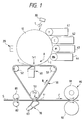
- FIG. 1 is a shematic view showing the main components of an image forming apparatus in a drawing showing a first embodiment of an image forming apparatus related to the present invention.
- the reference numeral 10 is a photosensitive drum, as an image carrier, rotated in the direction of the arrow A in the drawing by a drive means not shown in the drawing.
- charging means 20 On the circumference of the photosensitive drum 10, charging means 20, exposing means 30, developing means 41 (yellow), 42 (cyan), 43 (magenta) and 44 (black)for four colors and an intermediate transfer medium 50 as a first transfer means are disposed following the direction of rotation.
- the photosensitive drum and all the above-mentioned means are constructed by means of well-known technology.
- the intermediate transfer medium 50 is constructed of a conventional endless belt-like material, wrapped around drive rollers 51, 52 and 53, and driven circulatively in the direction of the arrow B in the drawing.
- the intermediate transfer medium 50 contacts the photosensitive drum 10 between the drive rollers 51 and 52.
- a first transfer means 60 is disposed on the opposite side of the contact portion (Tr1) and forms first transfer portion Tr1 at the contact portion of the photosensitive drum 10 and intermediate transfer medium 50.
- the intermediate transfer medium 50 contacts a recording medium as a second transfer medium S (paper etc.) at the outer circumferential surface of the portion wrapping onto the drive roller 53.
- a second transfer means 70 is disposed on the opposite side of the contact portion (Tr2), and forms second transfer portion Tr2 at the contact portion of the intermediate transfer medium 50 and second transfer medium S.
- a recording medium S is supplied to the transfer portion Tr2 by means of conveying rollers 81 and 82, and is conveyed in the direction of the arrow C.
- the reference numeral 90 is a fixing means, comprising a fixing roller 91 having an internal heat source and a pressure roller 92 pushed thereupon.
- the photosensitive drum 10 rotates in the direction of the arrow A, and its surface is uniformly charged by the charging means 20. After that, an electrostatic latent image is formed on the surface of the photosensitive drum 10 by means of scanning by such as a laser beam L generated from the exposing means 30, and this latent image is developed by yellow toner by means of the first color developing means 41.
- This toner image T is transferred from the photosensitive drum 10 to the surface of the intermediate transfer medium 50 by means of the effect of an electrical field applied by the first transfer means 60 at the first transfer portion Tr1.
- the surface of the photosensitive drum 10 is uniformly charged again by the charging means 20, an electrostatic latent image is formed on the surface of photosensitive drum 10 by means of scanning by such as a laser beam L generated from the exposing means 30, and this latent image is developed by cyan toner by means of the second color developing means 42.
- This toner image T is transferred to the surface of the intermediate transfer medium 50 at the first transfer portion Tr1.
- a magenta toner image developed by means of the third color developing means 43 is transferred to the surface of the intermediate transfer medium 50
- a black toner image developed by means of fourth color developing means 44 is transferred to the surface of intermediate transfer medium 50
- a full-color toner image is transferred to the surface of the intermediate transfer medium 50.
- This full-color toner image T' is transferred to the surface of the recording medium S from the intermediate transfer medium 50 by means of the effect of an electrical field applied by the second transfer means 70 at second transfer portion Tr2. Furthermore, recording medium S is conveyed at a prescribed timing with respect to the second transfer portion Tr2.
- the toner image T' is fixed on the surface of the recording medium S by the recording medium S passing through the fixing means 80.
- intermediate transfer medium 50 fulfills the role of a transfer medium in the first transfer portion Tr1, and fulfills the role of an image carrier in the second transfer portion Tr2.
- FIGS. 2(a) and 2(b) show the first transfer portion Tr1 and first transfer means 60
- FIG. 2(a) is a partial plan view (section a-a in FIG. 2(b))
- FIG. 2(b) is a partial cross-sectional view (cross section b-b in FIG. 2(a)).
- the first transfer means 60 has a film 61.
- This film 61 is supported by a support 63 via a thin plate-like supporting member 62 having electrical conductivity, and lightly contacts the back surface of the intermediate transfer medium 50. Then, this film 61 rises rapidly with respect to a contact portion 61a with the back surface of intermediate transfer medium 50 on the upstream side U of the direction of movement of the intermediate transfer medium 50 relative to the film , and slopes gently from the contact portion 61a in a continuous curve 61c on a downstream side D of the direction of movement.
- Supporting member 62 is in a state of electrical conductance with film 61, and an electric current is supplied to film 61 from a power source 64 via this supporting member 62.
- the support 63 is fixed into an image forming apparatus frame F by a screw 65, and the supporting member 62 is joined to the support 63 and film 61.
- a conductive adhesive or the like is utilized for the connection between the supporting member 62 and film 61.
- the film 61 itself allows the application of a transfer field between the photosensitive drum 10 and intermediate transfer medium 50, it is possible to employ various configurations: for example, a single-layer film (comprising a resistance layer 61A only) as shown in FIG. 3 (a); a two-layer film made of a resistance layer 61A and a surface layer 61B as shown in FIG. 3(b); a two-layer film made of a conductive layer 61C and a resistance layer 61A as shown in FIG. 3(c); and a three-layer film made of a conductive layer 61C, a resistance layer 61A and a surface layer 61B as shown in FIG. 3(d).
- a single-layer film comprising a resistance layer 61A only
- a two-layer film made of a resistance layer 61A and a surface layer 61B as shown in FIG. 3(b
- a two-layer film made of a conductive layer 61C and a resistance layer 61A as shown in FIG
- the resistance layer 61A contacts the intermediate transfer means 50 and the conductive layer 61C is connected to the supporting member 62.
- the surface layer 61B contacts the intermediate transfer medium 50 and the conductive layer 61C is connected to the supporting member 62.
- a dispersed conductive material film a conductive resin or a semiconductive resin or the like as the resistance layer 61A. Furthermore, it is also possible to employ a simple substance such as a metal thin place or thin film of stainless steel, steel, nickel or aluminum.
- a dispersed conductive material film a film comprising a substance belonging to groups a) and b) below dispersed / dissolved within a resin chosen from groups c) to f) is cited. Furthermore, it is possible to cite a substance belonging to groups a) and b) below dispersed / dissolved within a substance having rubber elasticity cited in either group g) or groups h) to j) below or the like.
- a substance chosen from group b) below is cited as the conductive resin.
- a substance chosen from group c) below is cited as the semiconductive resin.
- the conductive layer 61C has the role of supplying an electrical charge (electric current) from the supporting member 62 having electrical conductivity to the resistance layer 61A. Consequently, it has a lower resistance than that of the resistance layer 61A, and it does not matter if the layer thickness (film thickness) is small. It is possible to employ such as a metal vapor deposition film, a dispersed conductive material film or a conductive resin as conductive layer 61C. Vapour deposited metals and alloys such an aluminum, indium, nickel, tin and steel are cited as the metal vapor deposition film.
- a film comprising a substance belonging to groups a) and b) below dispersed / dissolved within a resin chosen from groups c) to f) is cited.
- a substance chosen from group b) below is cited as the conductive resin.
- the surface layer 61B plays the roles of, among others, protecting the film from wear or the like, preventing the exudation of low-molecular-weight components from a layer underneath the surface layer 61B, and increasing the releasability of the toner, and is a substance chosen from groups c) to f) of substances listed below. Furthermore, it is possible to cite a substance chosen from groups a) and b) below dispersed / dissolved within a resin cited in groups c) to f).
- Carbon blacks e.g. furnace black, acetylene black and carbon fillers
- metallic oxide powders e.g. ITO powder and SnO 2 powder
- metal or alloy powders e.g. Ag powder and Al powder
- salts e.g. quaternary ammonium salt and perchlorate
- Electrically conductive resins such as polyvinyl aniline, polyvinyl pyrrole, polydiacetylene, polyethyleneimine, and polymethyl methacrylate including quaternary ammonium salt.
- Resins such as ethyl cellulose, nitrocellulose, methoxymethylated nylon, ethoxymethylated nylon, copolymerized nylon, polyvinyl pyrrolidone and casein, or a mixture of these resins.
- Thermoplastic resins including acrylic resins such as polyacrylate and polymethacrylate; styrene resins such as polystyrene and poly-1-methylstyrene; butyral resin; polyvinyl chloride; polyvinylidene chloride; polyvinyl fluoride; polyvinylidene fluoride; polyester resin; polycarbonate resin; cellulose resin; polyarylate resin; polyethylene resin, nylon resin, and polypropylene resin; or a copolymer or mixture thereof.
- Water-soluble resins such as polyvinyl alcohol; polyaryl alcohol; polyvinyl pyrrolidone; polyvinylamine; polyarylamine; polyvinylacrylate; polyvinyl methacrylate; polyvinyl sulphuric acid; polylactic acid; casein; hydroxypropyl cellulose; starch; gum arabic; polyglutamic acid; polyaspartic acid; and nylon resin; or a copolymer or mixture thereof.
- Thermosetting resins such as epoxy resin; silicone resin; urethane resin; melamine resin; alkyd resin; polyimide resin; polyamide resin; and fluorine resin.
- Synthetic rubbers such as silicon rubber; fluorine rubber; fluorosilicon rubber; urethane rubber; acryl rubber; hydrin rubber; epichlorohydrin rubber; butadiene rubber; styrene-butadiene rubber; nitrile-butadiene rubber; isoprene rubber; chloroprene rubber; isobutylene-isoprene rubber; ethylene-propylene rubber; chlorosulfonated polyethylene; and thiokol, or a mixture thereof.
- Elastomer materials including styrol resin; vinyl chloride resin; polyurethane resin; polyethylene resin; methacrylic resin and the like.
- Soft foam materials such as polyurethane foam; polystyrene foam; polyethylene foam; elastomer foam; and rubber foam.
- a base is formed. It is possible to use a conductive layer or a resistance layer as described above for the base.
- Methods of preparing the base include a method wherein the substance constituting the base is thermally melted, is dispersed or mutually dissolved, and is extruded, thereby being molded into the form of a film; or a method wherein the substance constituting the base is dissolved in a solvent, is dispersed or mutually dissolved (is polymerized), and is extruded, thereby being molded into the form of a film.
- either one or a plurality of conductive layers are formed by a method wherein each substance is dissolved in a solvent, dispersed or dissolved (is polymerized), and is dip-coated or spray-coated.
- FIGS. 4(a) and 4(b) show the second transfer portion Tr2 and second transfer means 70
- FIG 4.(a) is a plan view (section a-a in FIG. 4(b))
- FIG. 4(b) is a cross-sectional view (cross section b-b in FIG. 4(a)).
- the second transfer means 70 has a film 71.
- the film 71 is supported by the support 73 via a supporting member 72 having electrical conductivity.
- the supporting member 72 is in electrical conductance with the film 71, and an electrical current is supplied to the film 71 from a power source 74 via the supporting member 72.
- the support 73 is fixed into the image forming apparatus frame F by a screw 75, and the supporting member 72 is joined to the support 73 and film 71.
- a conductive adhesive or the like is utilized for the connection between supporting member 72 and film 71.
- the intermediate transfer medium 50 fulfills the role of an image carrier in the second transfer portion Tr2.
- the support 73 is arranged separated from the intermediate transfer medium 50 by distance L.
- the film 71 is between the support 73 and intermediate transfer medium 50 capable of displacement, and contacts and disengages the recording medium S according to the presence or absence of electrostatic adsorptive force due to the supply or withdrawal of an electric current.
- the film 71 rises rapidly with respect to the contact portion 71a with the back surface of the recording medium S in an upstream direction U to the direction of movement of the recording medium S relative to the film 71, and slopes gently from the contact portion 71a with a continuous curve 71c in a downstream D to the direction of movement.
- the film 71 contacts the back surface of the recording medium S by means of electrostatic adsorptive force only at the time of the transfer operation, staining of the back surface of the recording medium S is prevented.
- the transfer pressure is heavy and the problem of center void (a phenomenon whereby an image loss occurs because the central portion of an image cannot be transferred) occurs, but according to the image forming apparatus of this embodiment, as the transfer pressure can be made light, it is possible to prevent the occurrence of center void.
- FIG. 5 is a schematic view showing the transfer portion of an image forming apparatus in a drawing showing the main components of the second embodiment of an image forming apparatus related to the present invention.
- the same reference numerals are attached to components which are the same as in the first embodiment described above.
- the point of difference between the second embodiment and the first embodiment described above is the cross-sectional shape of first transfer means 60, there are no changes with respect to the other points.
- the reference numeral 66 in FIG. 5 is a film, supported by a support 67 having electrical conductance, and lightly contacting the back surface of the intermediate transfer medium 50.
- the support 67 has a triangular-shaped cross-section, of which opposing portion 67a (opposing the intermediate transfer medium 50) is formed with an acute angle, and the film 66 is supported by the support 67 and rises steeply with respect to the contact portion 66a with the back surface of the intermediate transfer medium 50 an the upstream side U of the direction of movement of the intermediate transfer medium 50, and gently falls in a continuous curving line 66c from the contact portion 66a on the downstream side D of the direction of movement.
- the support 67 is in electrical conductance with the film 66, and an electrical current is supplied to the film 66 from a power source 64 via the support 67.
- FIG. 6 is a typical view showing the transfer portion of an image forming apparatus in a drawing showing the main components of a third embodiment of an image forming apparatus related to the present invention.
- the same reference numerals are attached to components which are the same as in the first embodiment described above.
- the point of difference between the third embodiment and the first embodiment described above is the cross-sectional shape of the first transfer means, there are no changes with respect to the other points.
- the reference numeral 68 in FIG. 6 is a film, supported by a flat plate-shaped support 69 having electrical conductance, and lightly contacting the back surface of the intermediate transfer medium 50.
- the film 68 rises steeply with respect to the contact portion 68a with the back surface of the intermediate transfer medium 50 on the upstream side U of the direction of movement of the intermediate transfer medium 50, and gently falls in a continuous curving line 68c from the contact portion 68a on the downstream side D of the direction of movement.
- the support 69 is in electrical conductance with the film 68, and an electrical currant is supplied to film 68 from a power source 64 via the support 69. Furthermore, it is possible to adopt the same construction for film 68 as that of film 61 in the first embodiment.
- the second transfer portion Tr2 of the first embodiment can also be used when an intermediate transfer medium 50 is not used and a toner image is transferred directly to the recording medium S from the photosensitive drum 10.
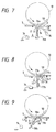
- FIG. 7 is a schematic view showing the transfer portion of an image forming apparatus in a drawing showing the main components of a fourth embodiment of an image forming apparatus related to the present invention.
- the same reference numerals are attached to components which are the same as in the first embodiment described above.
- the point of difference between the fourth embodiment and the first embodiment described above is the cross-sectional shape of the second transfer means, there are no changes with respect to the other points.
- the reference numeral 76 in FIG. 7 is a film with a cross section shaped substantially like an inverted hook, the base of which is supported by a support 76b having electrical conductivity.
- the Support 76b is in electrical conductance with the film 76, and through this support 76b, an electrical current is supplied to the film 76 from the power source 74.
- the support 76b is disposed separated by a gap L1 from the intermediate transfer medium 50.
- the film 76 is capable of displacement between the intermediate transfer medium 50 and support 76b, and contacts and disengages the recording medium S according to the presence or absence of electrostatic adsorptive force due to the supply or withdrawal of an electric current from the power source 74.
- film 76 rises rapidly with respect to a contact portion 76a with the back surface of the recording medium S on the upstream side U of the direction of movement of the recording medium S relative to the film, and slopes gently from the contact portion 76a in a continuous curve 76c on a downstream side D of the direction of movement.
- first transfer portion Tr1 of the first embodiment as the construction of the transfer portion; it can also be used when an intermediate transfer medium 50 is not used and a toner image is transferred directly to the recording medium S from the photosensitive drum 10 (please see the broken line in FIG. 7).
- FIG. 8 is a schematic view showing the transfer portion of an image forming apparatus in a drawing showing the main components of a fifth embodiment of an image forming apparatus related to the present invention.
- the same reference numerals are attached to components which are the same as in the first embodiment described above.
- the point of difference between the fifth embodiment and the first embodiment described above is the cross-sectional shape of the transfer means, there are no changes with respect to the other points.
- the reference numeral 77 in FIG. 8 is a film with a cross section shaped substantially like the letter "L", the base of which is supported by a support 77b having electrical conductivity.
- the support 77b is in electrical conductance with the film 77, and through this support 77b, an electrical current is supplied to the film 77 from the power source 74.
- the support 77b is disposed separated by a gap L2 from the intermediate transfer medium 50.
- the film 77 is capable of displacement between the intermediate transfer medium 50 and support 77b, and contacts and disengages recording medium S according to the presence or absence of electrostatic adsorptive force due to the supply or withdrawal of an electric current from the power source 74.
- film 77 rises rapidly with respect to a contact portion 77a with the back surface of the recording medium S on the upstream side U of the direction of movement of the recording medium S relative to the film, and slopes gently from the contact portion 77a in a continuous curve 77c on a downstream side D of the direction of movement.
- film 77 itself, while giving it the electrostatic adsorptive force effect described above, makes it possible to apply a transfer field between the intermediate transfer medium 50 and recording medium S, and it is possible to employ the same construction as the film 61 described above.
- first transfer portion Tr1 of the first embodiment as the construction of the transfer portion; it can also be used when an intermediate transfer medium 50 is not used and a toner image is transferred directly to recording medium S from the photosensitive drum 10 (please see the broken line in FIG. 8).
- FIG. 9 is a schematic view showing the transfer portion of an image forming apparatus in a drawing showing the main components of a sixth embodiment of an image forming apparatus related to the present invention.
- the same reference numerals are attached to components which are the same as in the first embodiment described above.
- the point of difference between the sixth embodiment and the first embodiment described above is the cross-sectional shape of the transfer means, there are no changes with respect to the other points.
- the reference numeral 78 in FIG. 9 is a film with a loop-shaped cross section, the base of which is supported by a support 78b having electrical conductivity.
- the support 78b is in electrical conductance with the film 78, and through this support 78b, an electrical current is supplied to film 78 from the power source 74.
- the support 78b is disposed separated by a gap L3 from the intermediate transfer medium 50.
- the film 78 is capable of displacement between the intermediate transfer medium 50 and support 78b, and contacts and disengages the recording medium S according to the presence or absence of electrostatic adsorptive force due to the supply or withdrawal of an electric current from the power source 74.
- the film 78 rises rapidly with respect to a contact portion 78a with the back surface of the recording medium S on the upstream side U of the direction of movement of the recording medium S relative to the film, and slopes gently from the contact portion 78a in a continuous curve 78c on a downstream side D of the direction of movement.
- first transfer portion Tr1 of the first embodiment as the construction of the transfer portion; it can also be used when an intermediate transfer medium 50 is not used and a toner image is transferred directly to the recording medium S from the photosensitive drum 10 (please see the broken line in FIG. 9).
- the transfer field rises rapidly on the upstream side of the contact portion, and falls gently on the downstream side of the contact portion, splashing of un-transferred toner on the upstream side of the contact portion and splashing of already transferred toner on the downstream side of the contact portion is suppressed.
- the film When an electrical current is supplied to the film, the film automatically contacts the back surface of the transfer medium due to the electrostatic adsorptive force, while passing this contact portion, the transfer field is applied between the image carrying member and the transfer medium, and when the electric current is not supplied, as the electrostatic adsorptive force disappears, the film automatically withdraws from the transfer medium.
- the film contacts the transfer medium by means of electrostatic adsorptive force, the contact pressure can be made extremely light, and a more favorable transfer condition can be obtained.
- the present invention provides a transfer means having a film lightly contacting a back surface of a transfer medium and applying a transfer field thereto.
- the film rises rapidly with respect to a contact portion with the back surface or the transfer medium on the upstream side of the direction or movement of the transfer medium relative to the film, and slopes gently from the contact portion in a continuous curve on a downstream side of the direction of movement.
- the film is capable of displacement between a support and an image carrier, and contacts and disengages the transfer medium according to the presence or absence of electrostatic adsorptive force due to the supply or withdrawal of an electric current.
Landscapes
- Physics & Mathematics (AREA)
- General Physics & Mathematics (AREA)
- Chemical & Material Sciences (AREA)
- Engineering & Computer Science (AREA)
- Nanotechnology (AREA)
- Health & Medical Sciences (AREA)
- Life Sciences & Earth Sciences (AREA)
- General Health & Medical Sciences (AREA)
- Molecular Biology (AREA)
- Crystallography & Structural Chemistry (AREA)
- Electrostatic Charge, Transfer And Separation In Electrography (AREA)
- Color Electrophotography (AREA)
Applications Claiming Priority (2)
| Application Number | Priority Date | Filing Date | Title |
|---|---|---|---|
| JP300696/95 | 1995-10-25 | ||
| JP30069695A JP3677839B2 (ja) | 1995-10-25 | 1995-10-25 | 画像形成装置 |
Publications (3)
| Publication Number | Publication Date |
|---|---|
| EP0770933A2 true EP0770933A2 (fr) | 1997-05-02 |
| EP0770933A3 EP0770933A3 (fr) | 1999-05-12 |
| EP0770933B1 EP0770933B1 (fr) | 2008-12-17 |
Family
ID=17887986
Family Applications (1)
| Application Number | Title | Priority Date | Filing Date |
|---|---|---|---|
| EP96117174A Expired - Lifetime EP0770933B1 (fr) | 1995-10-25 | 1996-10-25 | Appareil de formation d'images |
Country Status (4)
| Country | Link |
|---|---|
| US (2) | US5697033A (fr) |
| EP (1) | EP0770933B1 (fr) |
| JP (1) | JP3677839B2 (fr) |
| DE (1) | DE69637776D1 (fr) |
Families Citing this family (22)
| Publication number | Priority date | Publication date | Assignee | Title |
|---|---|---|---|---|
| JP3677839B2 (ja) * | 1995-10-25 | 2005-08-03 | セイコーエプソン株式会社 | 画像形成装置 |
| JP3267501B2 (ja) * | 1996-02-23 | 2002-03-18 | キヤノン株式会社 | 転写装置 |
| KR100411178B1 (ko) * | 2000-10-09 | 2003-12-18 | 한국화학연구원 | 신규 항균제와 이러한 항균제를 함유하는 항균탈취성 용액 |
| KR100395552B1 (ko) * | 2002-01-30 | 2003-08-25 | 삼성전자주식회사 | 균일한 닙이 형성되도록 하는 화상형성장치 |
| DE102005024380B4 (de) * | 2005-05-27 | 2007-05-16 | Oce Printing Systems Gmbh | Vorrichtung und Verfahren zum elektrischen Aufladen eines Transportbandes unter Verwendung einer Kontaktlippe aus einem Gummimaterial |
| KR101009221B1 (ko) * | 2005-11-11 | 2011-01-19 | 캐논 가부시끼가이샤 | 화상 형성 장치 |
| JP5311768B2 (ja) * | 2007-06-14 | 2013-10-09 | キヤノン株式会社 | 画像形成装置 |
| JP5311767B2 (ja) * | 2007-06-14 | 2013-10-09 | キヤノン株式会社 | 画像形成装置 |
| JP2008310059A (ja) * | 2007-06-14 | 2008-12-25 | Canon Inc | 画像形成装置 |
| JP5464797B2 (ja) * | 2007-09-05 | 2014-04-09 | キヤノン株式会社 | 画像形成装置 |
| JP5043805B2 (ja) | 2007-11-19 | 2012-10-10 | キヤノン株式会社 | 画像形成装置 |
| DE102009033905A1 (de) * | 2008-08-22 | 2010-02-25 | Heidelberger Druckmaschinen Ag | Farbwerks- und Feuchtwerksanalyse |
| JP5448260B2 (ja) * | 2008-09-30 | 2014-03-19 | Ntn株式会社 | 転写帯電部材および画像形成装置 |
| JP5436032B2 (ja) * | 2009-05-01 | 2014-03-05 | キヤノン株式会社 | 画像形成装置 |
| US8920916B2 (en) * | 2010-01-08 | 2014-12-30 | Nitto Denko Corporation | Sliding member and method of producing the same |
| JP5570233B2 (ja) | 2010-01-29 | 2014-08-13 | キヤノン株式会社 | 画像形成装置 |
| JP5495830B2 (ja) * | 2010-02-09 | 2014-05-21 | キヤノン株式会社 | 画像形成装置 |
| JP2013029769A (ja) * | 2011-07-29 | 2013-02-07 | Canon Inc | 画像形成装置 |
| JP5377722B2 (ja) * | 2012-08-10 | 2013-12-25 | キヤノン株式会社 | 画像形成装置 |
| JP5312653B2 (ja) * | 2012-08-10 | 2013-10-09 | キヤノン株式会社 | 画像形成装置 |
| US9042796B2 (en) * | 2013-09-03 | 2015-05-26 | Xerox Corporation | Transfer assist blade |
| US9268266B1 (en) | 2015-05-27 | 2016-02-23 | Xerox Corporation | Transfer assist blade |
Family Cites Families (8)
| Publication number | Priority date | Publication date | Assignee | Title |
|---|---|---|---|---|
| US3936174A (en) * | 1975-01-27 | 1976-02-03 | Xerox Corporation | Transfer roller with stationary internal electrode |
| US4341456A (en) * | 1980-06-27 | 1982-07-27 | Xerox Corporation | Transfer system for a xerographic reproduction machine |
| JP2707359B2 (ja) * | 1990-05-31 | 1998-01-28 | キヤノン株式会社 | 画像形成装置 |
| US5428429A (en) * | 1991-12-23 | 1995-06-27 | Xerox Corporation | Resistive intermediate transfer member |
| US5594538A (en) * | 1992-12-29 | 1997-01-14 | Canon Kabushiki Kaisha | Image forming apparatus having multi-layer transfer material bearing member with different coefficient of kinetic frictions between layers |
| JP3347376B2 (ja) * | 1992-12-29 | 2002-11-20 | キヤノン株式会社 | 画像形成装置 |
| JP3411335B2 (ja) * | 1993-07-02 | 2003-05-26 | 株式会社イノアックコーポレーション | 接触転写装置 |
| JP3677839B2 (ja) * | 1995-10-25 | 2005-08-03 | セイコーエプソン株式会社 | 画像形成装置 |
-
1995
- 1995-10-25 JP JP30069695A patent/JP3677839B2/ja not_active Expired - Fee Related
-
1996
- 1996-10-25 DE DE69637776T patent/DE69637776D1/de not_active Expired - Lifetime
- 1996-10-25 EP EP96117174A patent/EP0770933B1/fr not_active Expired - Lifetime
- 1996-10-25 US US08/736,203 patent/US5697033A/en not_active Expired - Fee Related
-
1997
- 1997-08-21 US US08/915,724 patent/US5893665A/en not_active Expired - Fee Related
Also Published As
| Publication number | Publication date |
|---|---|
| DE69637776D1 (de) | 2009-01-29 |
| US5697033A (en) | 1997-12-09 |
| US5893665A (en) | 1999-04-13 |
| EP0770933A3 (fr) | 1999-05-12 |
| EP0770933B1 (fr) | 2008-12-17 |
| JP3677839B2 (ja) | 2005-08-03 |
| JPH09120218A (ja) | 1997-05-06 |
Similar Documents
| Publication | Publication Date | Title |
|---|---|---|
| EP0770933B1 (fr) | Appareil de formation d'images | |
| US5617191A (en) | Toner conveyor roller and image forming apparatus having the same | |
| US6477348B2 (en) | Image forming apparatus | |
| CN100589044C (zh) | 成像设备 | |
| JP2010008641A (ja) | 画像形成装置 | |
| US20040223792A1 (en) | Method and apparatus for image forming capable of reducing mechanical stresses to developers during transportation for development | |
| US20070059029A1 (en) | Image-Forming Apparatus | |
| CN106227010A (zh) | 成像设备 | |
| US6684042B2 (en) | Charging device and image forming apparatus using the same | |
| CN1629741A (zh) | 具有间隔件的感光鼓和具有该感光鼓的电照相成像装置 | |
| JP2006163216A (ja) | 画像形成装置 | |
| JPH09160274A (ja) | 像担持体及びこれを用いた画像形成装置 | |
| EP0974877A2 (fr) | Appareil de formation d'images | |
| EP0685773B1 (fr) | Imagerie en couleur à haute stabilité à l'aide d'un rouleau de transfert | |
| JP3347376B2 (ja) | 画像形成装置 | |
| JP4589167B2 (ja) | 転写装置および画像形成装置 | |
| JP2808173B2 (ja) | 画像形成装置 | |
| JPH08137183A (ja) | カラー画像形成装置 | |
| JP3149300B2 (ja) | 現像装置 | |
| US6250743B1 (en) | Tandem type of direct printing apparatus using gating apertures for supplying toner | |
| JP2708148B2 (ja) | カラー画像形成方法 | |
| JP3641917B2 (ja) | 像担持体ユニット | |
| JP2002049212A (ja) | 画像形成装置 | |
| JP3052567B2 (ja) | 現像装置 | |
| JP3397587B2 (ja) | 転写装置 |
Legal Events
| Date | Code | Title | Description |
|---|---|---|---|
| PUAI | Public reference made under article 153(3) epc to a published international application that has entered the european phase |
Free format text: ORIGINAL CODE: 0009012 |
|
| AK | Designated contracting states |
Kind code of ref document: A2 Designated state(s): DE FR GB IT |
|
| PUAL | Search report despatched |
Free format text: ORIGINAL CODE: 0009013 |
|
| AK | Designated contracting states |
Kind code of ref document: A3 Designated state(s): DE FR GB IT |
|
| 17P | Request for examination filed |
Effective date: 19990628 |
|
| 17Q | First examination report despatched |
Effective date: 20010205 |
|
| GRAP | Despatch of communication of intention to grant a patent |
Free format text: ORIGINAL CODE: EPIDOSNIGR1 |
|
| GRAS | Grant fee paid |
Free format text: ORIGINAL CODE: EPIDOSNIGR3 |
|
| GRAA | (expected) grant |
Free format text: ORIGINAL CODE: 0009210 |
|
| AK | Designated contracting states |
Kind code of ref document: B1 Designated state(s): DE FR GB IT |
|
| REG | Reference to a national code |
Ref country code: GB Ref legal event code: FG4D |
|
| REF | Corresponds to: |
Ref document number: 69637776 Country of ref document: DE Date of ref document: 20090129 Kind code of ref document: P |
|
| PLBE | No opposition filed within time limit |
Free format text: ORIGINAL CODE: 0009261 |
|
| STAA | Information on the status of an ep patent application or granted ep patent |
Free format text: STATUS: NO OPPOSITION FILED WITHIN TIME LIMIT |
|
| 26N | No opposition filed |
Effective date: 20090918 |
|
| PGFP | Annual fee paid to national office [announced via postgrant information from national office to epo] |
Ref country code: FR Payment date: 20101020 Year of fee payment: 15 |
|
| PGFP | Annual fee paid to national office [announced via postgrant information from national office to epo] |
Ref country code: DE Payment date: 20101020 Year of fee payment: 15 |
|
| PGFP | Annual fee paid to national office [announced via postgrant information from national office to epo] |
Ref country code: IT Payment date: 20101021 Year of fee payment: 15 Ref country code: GB Payment date: 20101020 Year of fee payment: 15 |
|
| GBPC | Gb: european patent ceased through non-payment of renewal fee |
Effective date: 20111025 |
|
| REG | Reference to a national code |
Ref country code: FR Ref legal event code: ST Effective date: 20120629 |
|
| PG25 | Lapsed in a contracting state [announced via postgrant information from national office to epo] |
Ref country code: DE Free format text: LAPSE BECAUSE OF NON-PAYMENT OF DUE FEES Effective date: 20120501 |
|
| REG | Reference to a national code |
Ref country code: DE Ref legal event code: R119 Ref document number: 69637776 Country of ref document: DE Effective date: 20120501 |
|
| PG25 | Lapsed in a contracting state [announced via postgrant information from national office to epo] |
Ref country code: FR Free format text: LAPSE BECAUSE OF NON-PAYMENT OF DUE FEES Effective date: 20111102 Ref country code: GB Free format text: LAPSE BECAUSE OF NON-PAYMENT OF DUE FEES Effective date: 20111025 Ref country code: IT Free format text: LAPSE BECAUSE OF NON-PAYMENT OF DUE FEES Effective date: 20111025 |