EP0771475B1 - Element detecteur photosensible - Google Patents
Element detecteur photosensible Download PDFInfo
- Publication number
- EP0771475B1 EP0771475B1 EP96919747A EP96919747A EP0771475B1 EP 0771475 B1 EP0771475 B1 EP 0771475B1 EP 96919747 A EP96919747 A EP 96919747A EP 96919747 A EP96919747 A EP 96919747A EP 0771475 B1 EP0771475 B1 EP 0771475B1
- Authority
- EP
- European Patent Office
- Prior art keywords
- radiation
- layer
- detector element
- sensitive detector
- sensitive
- Prior art date
- Legal status (The legal status is an assumption and is not a legal conclusion. Google has not performed a legal analysis and makes no representation as to the accuracy of the status listed.)
- Expired - Lifetime
Links
- 230000005855 radiation Effects 0.000 title claims abstract description 74
- 230000005670 electromagnetic radiation Effects 0.000 claims abstract description 7
- 238000011156 evaluation Methods 0.000 claims abstract description 7
- 238000006243 chemical reaction Methods 0.000 claims abstract 2
- 239000004065 semiconductor Substances 0.000 claims description 24
- 239000012528 membrane Substances 0.000 claims description 20
- XUIMIQQOPSSXEZ-UHFFFAOYSA-N Silicon Chemical compound [Si] XUIMIQQOPSSXEZ-UHFFFAOYSA-N 0.000 claims description 17
- 229910052710 silicon Inorganic materials 0.000 claims description 17
- 239000010703 silicon Substances 0.000 claims description 17
- 239000000758 substrate Substances 0.000 claims description 11
- 239000002800 charge carrier Substances 0.000 claims description 9
- 229910052732 germanium Inorganic materials 0.000 claims description 2
- VYPSYNLAJGMNEJ-UHFFFAOYSA-N Silicium dioxide Chemical compound O=[Si]=O VYPSYNLAJGMNEJ-UHFFFAOYSA-N 0.000 claims 4
- 229910052681 coesite Inorganic materials 0.000 claims 2
- 229910052906 cristobalite Inorganic materials 0.000 claims 2
- 239000000377 silicon dioxide Substances 0.000 claims 2
- 229910052682 stishovite Inorganic materials 0.000 claims 2
- 229910052905 tridymite Inorganic materials 0.000 claims 2
- 229910052581 Si3N4 Inorganic materials 0.000 claims 1
- -1 germanium ions Chemical class 0.000 claims 1
- 230000035515 penetration Effects 0.000 abstract description 5
- 238000000034 method Methods 0.000 description 16
- 238000004519 manufacturing process Methods 0.000 description 13
- 239000000463 material Substances 0.000 description 12
- 229910004298 SiO 2 Inorganic materials 0.000 description 9
- 230000008569 process Effects 0.000 description 8
- 238000000926 separation method Methods 0.000 description 7
- QVGXLLKOCUKJST-UHFFFAOYSA-N atomic oxygen Chemical compound [O] QVGXLLKOCUKJST-UHFFFAOYSA-N 0.000 description 6
- 239000001301 oxygen Substances 0.000 description 6
- 229910052760 oxygen Inorganic materials 0.000 description 6
- 230000008901 benefit Effects 0.000 description 4
- 238000002513 implantation Methods 0.000 description 4
- 238000002161 passivation Methods 0.000 description 4
- ZOXJGFHDIHLPTG-UHFFFAOYSA-N Boron Chemical compound [B] ZOXJGFHDIHLPTG-UHFFFAOYSA-N 0.000 description 3
- 229910052796 boron Inorganic materials 0.000 description 3
- 230000001419 dependent effect Effects 0.000 description 3
- 238000005516 engineering process Methods 0.000 description 3
- 238000009792 diffusion process Methods 0.000 description 2
- 238000005530 etching Methods 0.000 description 2
- GNPVGFCGXDBREM-UHFFFAOYSA-N germanium atom Chemical group [Ge] GNPVGFCGXDBREM-UHFFFAOYSA-N 0.000 description 2
- 230000035945 sensitivity Effects 0.000 description 2
- 230000003595 spectral effect Effects 0.000 description 2
- 230000006641 stabilisation Effects 0.000 description 2
- 238000011105 stabilization Methods 0.000 description 2
- 230000007704 transition Effects 0.000 description 2
- RZVAJINKPMORJF-UHFFFAOYSA-N Acetaminophen Chemical compound CC(=O)NC1=CC=C(O)C=C1 RZVAJINKPMORJF-UHFFFAOYSA-N 0.000 description 1
- 229910001218 Gallium arsenide Inorganic materials 0.000 description 1
- 229910000530 Gallium indium arsenide Inorganic materials 0.000 description 1
- 241000511976 Hoya Species 0.000 description 1
- KWYUFKZDYYNOTN-UHFFFAOYSA-M Potassium hydroxide Chemical compound [OH-].[K+] KWYUFKZDYYNOTN-UHFFFAOYSA-M 0.000 description 1
- 229910008310 Si—Ge Inorganic materials 0.000 description 1
- 229910000831 Steel Inorganic materials 0.000 description 1
- CFOAUMXQOCBWNJ-UHFFFAOYSA-N [B].[Si] Chemical class [B].[Si] CFOAUMXQOCBWNJ-UHFFFAOYSA-N 0.000 description 1
- 238000010521 absorption reaction Methods 0.000 description 1
- 238000000137 annealing Methods 0.000 description 1
- 230000004888 barrier function Effects 0.000 description 1
- 238000010923 batch production Methods 0.000 description 1
- 230000015572 biosynthetic process Effects 0.000 description 1
- 230000000903 blocking effect Effects 0.000 description 1
- 239000012876 carrier material Substances 0.000 description 1
- 230000008859 change Effects 0.000 description 1
- 239000013078 crystal Substances 0.000 description 1
- 230000000694 effects Effects 0.000 description 1
- 230000005684 electric field Effects 0.000 description 1
- 230000007613 environmental effect Effects 0.000 description 1
- 238000000407 epitaxy Methods 0.000 description 1
- 238000011049 filling Methods 0.000 description 1
- 239000007789 gas Substances 0.000 description 1
- 239000011521 glass Substances 0.000 description 1
- PCHJSUWPFVWCPO-UHFFFAOYSA-N gold Chemical compound [Au] PCHJSUWPFVWCPO-UHFFFAOYSA-N 0.000 description 1
- 239000010931 gold Substances 0.000 description 1
- 229910052737 gold Inorganic materials 0.000 description 1
- 238000010438 heat treatment Methods 0.000 description 1
- 229910052751 metal Inorganic materials 0.000 description 1
- 239000002184 metal Substances 0.000 description 1
- 229910021421 monocrystalline silicon Inorganic materials 0.000 description 1
- 238000005457 optimization Methods 0.000 description 1
- 238000002360 preparation method Methods 0.000 description 1
- 239000005297 pyrex Substances 0.000 description 1
- 238000006862 quantum yield reaction Methods 0.000 description 1
- 241000894007 species Species 0.000 description 1
- 238000001228 spectrum Methods 0.000 description 1
- 238000004544 sputter deposition Methods 0.000 description 1
- 238000010025 steaming Methods 0.000 description 1
- 239000010959 steel Substances 0.000 description 1
Images


Classifications
-
- H—ELECTRICITY
- H10—SEMICONDUCTOR DEVICES; ELECTRIC SOLID-STATE DEVICES NOT OTHERWISE PROVIDED FOR
- H10F—INORGANIC SEMICONDUCTOR DEVICES SENSITIVE TO INFRARED RADIATION, LIGHT, ELECTROMAGNETIC RADIATION OF SHORTER WAVELENGTH OR CORPUSCULAR RADIATION
- H10F77/00—Constructional details of devices covered by this subclass
- H10F77/10—Semiconductor bodies
- H10F77/14—Shape of semiconductor bodies; Shapes, relative sizes or dispositions of semiconductor regions within semiconductor bodies
- H10F77/147—Shapes of bodies
-
- H—ELECTRICITY
- H10—SEMICONDUCTOR DEVICES; ELECTRIC SOLID-STATE DEVICES NOT OTHERWISE PROVIDED FOR
- H10F—INORGANIC SEMICONDUCTOR DEVICES SENSITIVE TO INFRARED RADIATION, LIGHT, ELECTROMAGNETIC RADIATION OF SHORTER WAVELENGTH OR CORPUSCULAR RADIATION
- H10F30/00—Individual radiation-sensitive semiconductor devices in which radiation controls the flow of current through the devices, e.g. photodetectors
- H10F30/20—Individual radiation-sensitive semiconductor devices in which radiation controls the flow of current through the devices, e.g. photodetectors the devices having potential barriers, e.g. phototransistors
- H10F30/21—Individual radiation-sensitive semiconductor devices in which radiation controls the flow of current through the devices, e.g. photodetectors the devices having potential barriers, e.g. phototransistors the devices being sensitive to infrared, visible or ultraviolet radiation
- H10F30/22—Individual radiation-sensitive semiconductor devices in which radiation controls the flow of current through the devices, e.g. photodetectors the devices having potential barriers, e.g. phototransistors the devices being sensitive to infrared, visible or ultraviolet radiation the devices having only one potential barrier, e.g. photodiodes
- H10F30/221—Individual radiation-sensitive semiconductor devices in which radiation controls the flow of current through the devices, e.g. photodetectors the devices having potential barriers, e.g. phototransistors the devices being sensitive to infrared, visible or ultraviolet radiation the devices having only one potential barrier, e.g. photodiodes the potential barrier being a PN homojunction
-
- H—ELECTRICITY
- H10—SEMICONDUCTOR DEVICES; ELECTRIC SOLID-STATE DEVICES NOT OTHERWISE PROVIDED FOR
- H10F—INORGANIC SEMICONDUCTOR DEVICES SENSITIVE TO INFRARED RADIATION, LIGHT, ELECTROMAGNETIC RADIATION OF SHORTER WAVELENGTH OR CORPUSCULAR RADIATION
- H10F39/00—Integrated devices, or assemblies of multiple devices, comprising at least one element covered by group H10F30/00, e.g. radiation detectors comprising photodiode arrays
- H10F39/10—Integrated devices
- H10F39/12—Image sensors
- H10F39/199—Back-illuminated image sensors
-
- H—ELECTRICITY
- H10—SEMICONDUCTOR DEVICES; ELECTRIC SOLID-STATE DEVICES NOT OTHERWISE PROVIDED FOR
- H10F—INORGANIC SEMICONDUCTOR DEVICES SENSITIVE TO INFRARED RADIATION, LIGHT, ELECTROMAGNETIC RADIATION OF SHORTER WAVELENGTH OR CORPUSCULAR RADIATION
- H10F71/00—Manufacture or treatment of devices covered by this subclass
- H10F71/121—The active layers comprising only Group IV materials
-
- Y—GENERAL TAGGING OF NEW TECHNOLOGICAL DEVELOPMENTS; GENERAL TAGGING OF CROSS-SECTIONAL TECHNOLOGIES SPANNING OVER SEVERAL SECTIONS OF THE IPC; TECHNICAL SUBJECTS COVERED BY FORMER USPC CROSS-REFERENCE ART COLLECTIONS [XRACs] AND DIGESTS
- Y02—TECHNOLOGIES OR APPLICATIONS FOR MITIGATION OR ADAPTATION AGAINST CLIMATE CHANGE
- Y02E—REDUCTION OF GREENHOUSE GAS [GHG] EMISSIONS, RELATED TO ENERGY GENERATION, TRANSMISSION OR DISTRIBUTION
- Y02E10/00—Energy generation through renewable energy sources
- Y02E10/50—Photovoltaic [PV] energy
- Y02E10/547—Monocrystalline silicon PV cells
-
- Y—GENERAL TAGGING OF NEW TECHNOLOGICAL DEVELOPMENTS; GENERAL TAGGING OF CROSS-SECTIONAL TECHNOLOGIES SPANNING OVER SEVERAL SECTIONS OF THE IPC; TECHNICAL SUBJECTS COVERED BY FORMER USPC CROSS-REFERENCE ART COLLECTIONS [XRACs] AND DIGESTS
- Y02—TECHNOLOGIES OR APPLICATIONS FOR MITIGATION OR ADAPTATION AGAINST CLIMATE CHANGE
- Y02P—CLIMATE CHANGE MITIGATION TECHNOLOGIES IN THE PRODUCTION OR PROCESSING OF GOODS
- Y02P70/00—Climate change mitigation technologies in the production process for final industrial or consumer products
- Y02P70/50—Manufacturing or production processes characterised by the final manufactured product
Definitions
- the present invention relates to a radiation-sensitive detector element.
- Known radiation-sensitive detector elements are used to convert electromagnetic radiation signals into electrical signals.
- detector elements exist manifold Applications. Mention should be made in this context about the use in the scanning unit of photoelectric position measuring devices. There, the intended detector elements are used to detect the amplitude modulated Radiation signals at the relative offset of a scale graduation and a scanning plate.
- the scanning unit that is, there are certain Requirements for the radiation-sensitive detector elements used therein.
- the simplest possible production of used components, in particular the detector elements desirable.
- the usual radiation-sensitive detector elements have an active Area in which layers with different carrier concentrations are arranged adjacent, for example, semiconductor layers different doping. These are, for example, pn junctions, in which within an active area or within a forming space charge zone by the incident electromagnetic Radiation-free charge carriers are generated. So there are commercial Silicon-based photoelements made of n-doped silicon, in its surface a thin layer of p-doped silicon was diffused. The mentioned active area, in which the incidence of radiation, a charge carrier separation takes place, is just below the radiation-sensitive Surface. To the thus generated electrical signals to a To transmit evaluation circuit, are arranged on the detector element Contact elements or electrodes required.
- radiation-sensitive detector elements constructed in this way can now be integrated in the scanning unit, for example, in a printed circuit board on which, in addition, parts of the downstream evaluation electronics are arranged. It thus provides an education of the detector elements as so-called SMD elements (Surface Mounted Devices). This refers to miniaturized components that can be mounted directly on the surface of printed circuit boards or other substrates. In such an embodiment of the radiation-sensitive detector elements, however, certain requirements result in particular in the contacting. It proves to be advantageous if the detector elements are provided on the side with suitable terminal contacts, which is arranged opposite to the radiation-sensitive surface. Such a back contact is known in principle for solar cells, for example, from US Pat. No. 4,897,123 or EP 0 452 588.
- Photoelements and IR detector elements arranged at the back Contact electrodes are further from the publications R.S.Sussmann et al. Ultra Low Capacitance Flip Chip Bonded GalnAs PIN Photodetector For Long-Wavelength High-Data-Rate Fiber-Optic Systems ", Electronics Letters July 1985 Vol. 21, no. 14, pp. 593-595 and "SDI needs Age detector's mission ", Photonics Spectra, January 1986, p. 86, 88. Details for the production of such detector elements can be found in however, not these publications.
- a contactable solar cell is also known from US 4,838,952 known.
- holes are made in the base substrate from the back introduced and filled with conductive bonding material. In this case, the process is problematic or production-technically complicated the introduction of the holes in the base substrate.
- the object of the present invention is to provide a radiation-sensitive Detector element to be installed, which can be mounted using the SMD technology and is easy or inexpensive to manufacture. Demands are required in particular a way of contacting on the page, the is disposed opposite to that surface to which the incident radiation impinges.
- the inventive design of the radiation-sensitive detector element now allows the SMD mounting on a printed circuit board, since a contacting of the detector element from the back is possible, ie from the side which is arranged opposite to the radiation-sensitive side.
- the mentioned requirements with regard to the desired small space requirement can thus be met.
- there are advantages in the mass production of such devices if they can be made in so-called batch processes analogous to semiconductor manufacturing. In this case, a large number of identical components will be produced simultaneously on a single carrier substrate, for example made of silicon.
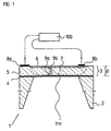
- FIG. 1 shows a first embodiment of the radiation-sensitive detector element (1) according to the invention in a lateral sectional representation.
- This comprises a carrier structure (2) on which a layer arrangement (3) having a plurality of different layers (5, 6) is applied, in the illustrated embodiment with two different layers (5, 6).
- the upper side of the detector element (1) is provided with two contact elements (8a, 8b).
- As material for the contact elements (8a, 8b) gold is provided in the illustrated variant. Accordingly, in the illustration of FIG. 1, the electromagnetic radiation (h ⁇ ) to be detected acts on the lower side of the detector element (1), ie the underside acts as the actual radiation-sensitive surface.
- the contact elements (8a, 8b) for connecting the detector element (1) with a schematically illustrated, downstream evaluation circuit (100), however, are provided on the upper side, ie on the side which is arranged opposite to the radiation-sensitive side. This arrangement is suitable, as explained above, in particular for the desired SMD mounting of the component on a printed circuit board and is made possible by the measures according to the invention described below.
- the layer arrangement (3) located on the support structure (2) comprises two contiguous layers (5, 6) or layer areas in which different Charge carriers each present in a defined concentration are.
- active area (7) In the boundary region between the two layers (5, 6) forms a Blocking, hereinafter referred to as active area (7) and which is shown enlarged in the illustration of Figure 1.
- active Area (7) of the layer arrangement (3) results in the incidence of the electromagnetic Radiation (h ⁇ ) is a generation of charge carrier pairs (9a, 9b), in turn, as electrical signals in the downstream evaluation circuit (100) can be detected.
- a further layer (4) is provided, which is formed as a SiO 2 layer and whose function will be explained in more detail in the course of the description.
- this layer (4) must of course be permeable to the respective radiation wavelength ⁇ .
- the incident radiation (h ⁇ ) usually strikes the component from the opposite side, ie on the side of the generally thinner of the two semiconductor layers (6), for which reason a contacting of the rear side and thus the desired SMD mounting is not possible.
- the detector element (1) can be acted upon by the actual "backside” with the radiation (h ⁇ ) to be detected. Accordingly, the electromagnetic radiation (h ⁇ ) initially strikes the thicker (5) of the two semiconductor layers of the pn junction, before the generation of charge carriers (9a, 9b) takes place in the active region (7).
- the position of the active region (7) of the radiation-sensitive detector element (1) must be set defined relative to the surface sensitive to steels.
- the doping concentrations in the two adjoining layers (5, 6) are preferably varied. Depending on the selected concentration, the active region (7) forms suitable.
- the penetration depth of the radiation (h ⁇ ) to be detected must therefore be sufficient to allow the charge carrier separation in the active region (7), even if initially the thicker (5) of the two semiconductor layers (5, 6) will pass through, ie the radiation incidence from this direction he follows.
- the thickness d of the layer assembly (3) was selected to be so thin that the conditions mentioned are met, ie the charge carrier separation in the active region (7). Accordingly, in this embodiment, the active region (7) occupies almost the entire thickness of the layer arrangement (3). Since the layer (4) provided below the layer arrangement (3) is designed to be transparent to the incident radiation (h ⁇ ), its thickness is of secondary importance in this context.
- the parameters to be selected change analogously with other radiation wavelengths or other materials. That's the way it is about possible to use thicker layer arrangements, in which the active area does not make up the entire layer thickness, but relative to radiation-sensitive surface as a function of the radiation wavelength is set appropriately. It is crucial again that the penetration depth the radiation to be detected is sufficient in any case through the thicker layer into the active area or in the forming barrier layer or space charge zone of the adjacently arranged To arrive at layers.
- the two semiconductor layers (5, 6) or the active region (7) are separated from the carrier structure (2) by a separating layer (4).
- the separating layer is formed as a SiO 2 layer, which is permeable to the wavelength to be detected of 830 nm.
- this separation layer (4) functions as an etch stop layer.
- the generation of this layer takes place in the so-called SIMOX process (separation by implanted oxygen).
- SIMOX process separation by implanted oxygen
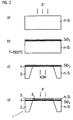
- FIG. 2 a shows a first method step of the production process, in which an oxygen implantation takes place into an n-doped, monocrystalline silicon substrate.
- FIG. 2 a shows a first method step of the production process, in which an oxygen implantation takes place into an n-doped, monocrystalline silicon substrate.
- the oxygen introduced just below the surface is tempered in a process of several hours at high temperatures of about 1300.degree.
- Typical thicknesses of the SiO 2 layer are on the order of several hundred nm (nanometers). The distance of the introduced layer from the overlying surface is also several hundred nm.
- the SiO 2 layer is now used as a release layer during an etching process in which by means of potassium hydroxide (KOH) of the lower part of the Si substrate to the SiO 2 separation layer or ⁇ tzstop Anlagen is selectively etched away, so that the 1 recognizable carrier structure (2) results, which mechanically stabilizes the complete detector element (1).
- KOH potassium hydroxide
- the support structure (2) is therefore cylindrical in shape; Of course, other geometries are feasible.
- the central, etched-away region of the detector element (1) with the delimiting SiO 2 layer subsequently acts as a radiation-sensitive surface.
- a filling material (not shown) which is transparent to the radiation to be detected and effects additional mechanical stabilization of the detector element (1).
- a spatially limited p-doped zone (6) of small thickness is finally introduced by means of known diffusion techniques into the thin silicon layer located above the separating layer, so that the structure of the layer arrangement already described with reference to FIG. Typical thicknesses of this layer are approximately in the range of several hundred nm.
- the final contacting of the top with the contact electrodes which is done via known bonding process in the form of sputtering or steaming.
- the thickness of the layer arrangement and thus also the Position of the active area relative to the radiation-sensitive surface adjust in the desired manner. This is especially for customization the thickness of the layer arrangement to the penetration depth of the used electromagnetic radiation of advantage, since such a simple Possibility for wavelength-optimized dimensioning results.
- the active one Area within the layer arrangement is thus always in one of the wavelength - dependent penetration depth adapted distance from the radiation-sensitive surface.
- the required p and n doping of the two layers takes place after the epitaxy process by appropriate Diffusion method in which in spatially separated areas of Layer arrangement introduced the different charge carriers defined become.
- an optimization of the detector element according to the invention can be at radiation to be detected in the infrared spectral range also achieve this when in the epitaxially grown silicon layer additionally introduced germanium atoms in a defined concentration so that a Si-Ge superlattice results.
- this spectral range can the detector element sensitivity thus on the corresponding Advantageously influence the concentration of introduced germanium.
- the thickness d of the layer arrangement (33) with the two differently doped semiconductor layers (35, 36) and the active region (37) is dimensioned such that the radiation-sensitive surface of the detector element (31) lies opposite that surface at which the contact elements (38a, 38b) are arranged in the form of contact electrodes.
- the layer arrangement (33) with the active region (7) is now designed as a correspondingly thin membrane. The required doping of the membrane (33), ie the formation of p- and n-doped layers or regions is already contained in the membrane (33) produced according to the requirements.
- a transparent passivation layer (34) is furthermore arranged in the illustrated embodiment of FIG.
- This passivation layer (34) serves to stabilize the electrical properties of the membrane (33) or of the component, ie for protection against a wide variety of environmental influences.
- Suitable passivation layers (34) are, for example, SiO 2 or Si 3 N 4 , which can each be deposited from the gas phase onto the corresponding surface.
- the membrane (33) including the passivation layer (34) on a, for example, cylindrical support member (32) to be arranged it also proves to be advantageous if the support element (32) used has the same coefficient of thermal expansion as the membrane (33), in order to avoid any mechanical stresses that may occur during heating.
- a carrier element (32) made of silicon is suitable with regard to equal thermal expansion coefficients; Alternatively, the use of Pyrex would be possible.
- the most stable possible mechanical connection between the membrane (33) and the carrier element (32) is advantageous in order to ensure the stability of the detector element (31) against vibrations and the like.
- connection technology for this purpose is the so-called “anodic bonding", in which under the influence of defined temperatures and / or electric fields, a connection with crystalline transition structures can be realized.
- Suitable support materials based on silicon for bonding with silicon membranes are offered for example by the company HOYA .
- a further embodiment of the radiation-sensitive invention Detector element show the figures 4a and 4b.
- the illustrated Variant differs from that of Figure 3 only in terms the selected type of contact and the shape of the detector element (51).
- the two contact elements (58a, 58b) in each case over a large area on a cross-sectionally square Perform detector element (51).
- This is opposite on the opposite Surface arranged square to the radiation incidence side formed first contact electrode (58b) with one of the two Layer regions (55, 56) of different doping connected.
- the second Contact electrode (58a) is annular around the first contact electrode (58b) arranged and connected to the second layer region (55).
- Such large-area contact can be possibly existing, locally avoid different sensitivities of the detector element (51).
- alternative geometries for the large area running Contact electrodes possible, approximately rotationally symmetrical Contact electrodes etc.
Landscapes
- Light Receiving Elements (AREA)
- Measurement Of Radiation (AREA)
Claims (12)
- Elément détecteur (1; 31; 51) sensible au rayonnement, comprenantcaractérisé en ce que l'agencement des éléments de contact (8a, 8b; 38a, 38b; 58a, 58b) se trouve sur la face de l'élément détecteur (1; 31; 51) qui est éloignée du rayonnement incident (hν) et est en contact planaire avec les différentes zones de couche (5, 6; 25, 26; 35, 36; 55; 56).une zone active (7; 27; 37; 57) qui est formée entre deux zones de couche (5, 6; 25, 26; 35, 36; 55, 56) contiguës d'un système de couches (3; 33; 53) ayant des porteurs de charge différents, et à l'intérieur de laquelle a lieu une conversion du rayonnement électromagnétique incident (hν) en signaux électriques, etau moins deux éléments de contact (8a, 8b; 38a, 38b; 58a; 58b) pour connecter l'élément détecteur (1; 31; 51) à un circuit de traitement (100), les éléments de contact (8a, 8b; 38a, 38b; 58a, 58b) étant montés sur une surface, en étant en contact avec les différentes zones de couche (5, 6; 25, 26; 35, 36; 55, 56), qui est située à l'opposé de la surface sensible au rayonnement, sur laquelle tombe le rayonnement incident (hν),
- Elément détecteur (1; 31; 51) sensible au rayonnement selon la revendication 1, caractérisé en ce que le système de couches (3; 33; 53), dans la direction du rayonnement incident (hν), est pourvu d'une couche (4; 54) qui est transparente audit rayonnement incident (hν).
- Elément détecteur (1; 31; 51) sensible au rayonnement selon la revendication 2, caractérisé en ce que la couche (4; 54) est réalisée comme couche SiO2.
- Elément détecteur (1; 31; 51) sensible au rayonnement selon la revendication 1, caractérisé en ce que le système de couches (3; 33; 53) est réalisé sous forme de couche de silicium obtenue par croissance épitaxiale, qui présente au moins deux zones de couche (5, 6; 25, 26; 35, 36; 55, 56) ayant des dopages différents.
- Elément détecteur (1; 31; 51) sensible au rayonnement selon la revendication 4, caractérisé en ce que la couche de silicium obtenue par croissance épitaxiale contient des ions de germanium.
- Elément détecteur (1; 31; 51) sensible au rayonnement selon la revendication 1, caractérisé en ce que le système de couches (33) est conformé en membrane à semi-conducteurs (d) mince, qui présente des zones de couche (35, 36) ayant des dopages différents.
- Elément détecteur (1; 31; 51) sensible au rayonnement selon la revendication 1 ou 6, caractérisé en ce que la surface tournée vers le rayonnement incident (hν) est pourvue d'une couche de passivation (34) perméable au rayonnement, qui est destinée à stabiliser les propriétés électriques.
- Elément détecteur (1; 31; 51) sensible au rayonnement selon la revendication 7, caractérisé en ce que la couche de passivation (34) est réalisée sous forme de couche SiO2 ou de couche Si3N4.
- Elément détecteur (31) sensible au rayonnement selon la revendication 6, caractérisé en ce que la membrane à semi-conducteurs (33) est disposée sur un substrat support (32) qui présente le même coefficient de dilatation thermique que la membrane à semi-conducteurs.
- Elément détecteur (51) sensible au rayonnement selon la revendication 1, caractérisé en ce qu'au moins un des éléments de contact (58a, 58b) est réalisé sous la forme d'une zone de connexion plane.
- Elément détecteur (51) sensible au rayonnement selon la revendication 10, caractérisé en ce que l'une des deux zones de couche (55, 56) du système de couches (53) présente une surface de base qui est plus grande que celle de l'autre zone de couche (55, 56), et que la zone de couche (55, 56) plus grande est pourvue d'une zone de connexion (58a, 58b) plane qui est connectée via un élément de contact (58a, 58b) supplémentaire au circuit de traitement branché à la suite.
- Utilisation d'un élément détecteur (1; 31; 51) sensible au rayonnement selon une des revendications précédentes dans l'unité de palpage d'un dispositif de mesure de position optoélectronique.
Applications Claiming Priority (3)
| Application Number | Priority Date | Filing Date | Title |
|---|---|---|---|
| DE19518423 | 1995-05-19 | ||
| DE19518423 | 1995-05-19 | ||
| PCT/EP1996/001976 WO1996036999A1 (fr) | 1995-05-19 | 1996-05-09 | Element detecteur photosensible et son procede de production |
Publications (2)
| Publication Number | Publication Date |
|---|---|
| EP0771475A1 EP0771475A1 (fr) | 1997-05-07 |
| EP0771475B1 true EP0771475B1 (fr) | 2005-12-21 |
Family
ID=7762359
Family Applications (1)
| Application Number | Title | Priority Date | Filing Date |
|---|---|---|---|
| EP96919747A Expired - Lifetime EP0771475B1 (fr) | 1995-05-19 | 1996-05-09 | Element detecteur photosensible |
Country Status (6)
| Country | Link |
|---|---|
| US (1) | US5852322A (fr) |
| EP (1) | EP0771475B1 (fr) |
| JP (1) | JPH10508987A (fr) |
| AT (1) | ATE313857T1 (fr) |
| DE (2) | DE19618593A1 (fr) |
| WO (1) | WO1996036999A1 (fr) |
Families Citing this family (42)
| Publication number | Priority date | Publication date | Assignee | Title |
|---|---|---|---|---|
| EP0871228A3 (fr) * | 1997-04-09 | 2001-10-24 | Matsushita Electric Industrial Co., Ltd. | Substrat semi-conducteur, dispositif semi-conducteur et procédé de fabrication |
| US6005276A (en) * | 1997-11-12 | 1999-12-21 | Advanced Photonix, Inc. | Solid state photodetector with light-responsive rear face |
| KR100394296B1 (ko) * | 1998-04-13 | 2003-08-09 | 인텔 코오퍼레이션 | 집적회로에서의 광 클록 분배 방법 및 장치 |
| JP4131998B2 (ja) * | 1998-04-30 | 2008-08-13 | 佐々木 実 | 透明な半導体受光素子およびその製造方法 |
| US5990490A (en) * | 1998-06-29 | 1999-11-23 | Miracle Technology Co., Ltd. | Optical electronic IC capable of photo detection |
| DE19834090A1 (de) | 1998-07-29 | 2000-02-03 | Heidenhain Gmbh Dr Johannes | Optoelektronische Sende- und Empfangseinheit |
| DE19859669A1 (de) | 1998-12-23 | 2000-06-29 | Heidenhain Gmbh Dr Johannes | Integrierter optoelektronischer Sensor und Verfahren zu dessen Herstellung |
| DE19917950A1 (de) * | 1999-04-21 | 2000-10-26 | Heidenhain Gmbh Dr Johannes | Integrierter optoelektronischer Dünnschichtsensor und Verfahren zu dessen Herstellung |
| AUPR174800A0 (en) * | 2000-11-29 | 2000-12-21 | Australian National University, The | Semiconductor processing |
| IL162190A0 (en) | 2001-11-29 | 2005-11-20 | Origin Energy Solar Pty Ltd | Semiconductor texturing process |
| EP1835539B1 (fr) * | 2002-08-09 | 2012-10-31 | Hamamatsu Photonics K.K. | Réseau photodiode et son procédé de fabrication |
| US20040169248A1 (en) * | 2003-01-31 | 2004-09-02 | Intevac, Inc. | Backside thinning of image array devices |
| US7042060B2 (en) * | 2003-01-31 | 2006-05-09 | Intevac, Inc. | Backside thinning of image array devices |
| EP1652237B1 (fr) * | 2003-01-31 | 2011-06-01 | Intevac, Inc. | Amincissement de face arriere de dispositifs a reseau d'images |
| US7005637B2 (en) * | 2003-01-31 | 2006-02-28 | Intevac, Inc. | Backside thinning of image array devices |
| JP4220818B2 (ja) | 2003-03-27 | 2009-02-04 | 浜松ホトニクス株式会社 | ホトダイオードアレイおよびその製造方法並びに放射線検出器 |
| US20040183003A1 (en) * | 2003-03-21 | 2004-09-23 | Mohammad Eslamy | Localized hermetic sealing of a power monitor on a planar light circuit |
| JP2005045073A (ja) * | 2003-07-23 | 2005-02-17 | Hamamatsu Photonics Kk | 裏面入射型光検出素子 |
| JP4499385B2 (ja) * | 2003-07-29 | 2010-07-07 | 浜松ホトニクス株式会社 | 裏面入射型光検出素子及び裏面入射型光検出素子の製造方法 |
| JP4499386B2 (ja) | 2003-07-29 | 2010-07-07 | 浜松ホトニクス株式会社 | 裏面入射型光検出素子の製造方法 |
| JP2005167090A (ja) * | 2003-12-04 | 2005-06-23 | Hamamatsu Photonics Kk | 半導体受光素子及びその製造方法 |
| US20050137187A1 (en) * | 2003-12-23 | 2005-06-23 | Souers Andrew J. | Antagonists of melanin concentrating hormone effects on the melanin concentrating hormone receptor |
| US9543356B2 (en) * | 2009-03-10 | 2017-01-10 | Globalfoundries Inc. | Pixel sensor cell including light shield |
| US10197501B2 (en) | 2011-12-12 | 2019-02-05 | Kla-Tencor Corporation | Electron-bombarded charge-coupled device and inspection systems using EBCCD detectors |
| US9496425B2 (en) * | 2012-04-10 | 2016-11-15 | Kla-Tencor Corporation | Back-illuminated sensor with boron layer |
| JP5966157B2 (ja) * | 2012-06-18 | 2016-08-10 | パナソニックIpマネジメント株式会社 | 赤外線検出装置 |
| US9601299B2 (en) | 2012-08-03 | 2017-03-21 | Kla-Tencor Corporation | Photocathode including silicon substrate with boron layer |
| US9426400B2 (en) | 2012-12-10 | 2016-08-23 | Kla-Tencor Corporation | Method and apparatus for high speed acquisition of moving images using pulsed illumination |
| US9478402B2 (en) | 2013-04-01 | 2016-10-25 | Kla-Tencor Corporation | Photomultiplier tube, image sensor, and an inspection system using a PMT or image sensor |
| US9347890B2 (en) | 2013-12-19 | 2016-05-24 | Kla-Tencor Corporation | Low-noise sensor and an inspection system using a low-noise sensor |
| US9748294B2 (en) | 2014-01-10 | 2017-08-29 | Hamamatsu Photonics K.K. | Anti-reflection layer for back-illuminated sensor |
| US9410901B2 (en) | 2014-03-17 | 2016-08-09 | Kla-Tencor Corporation | Image sensor, an inspection system and a method of inspecting an article |
| US9767986B2 (en) | 2014-08-29 | 2017-09-19 | Kla-Tencor Corporation | Scanning electron microscope and methods of inspecting and reviewing samples |
| US9860466B2 (en) | 2015-05-14 | 2018-01-02 | Kla-Tencor Corporation | Sensor with electrically controllable aperture for inspection and metrology systems |
| US10748730B2 (en) | 2015-05-21 | 2020-08-18 | Kla-Tencor Corporation | Photocathode including field emitter array on a silicon substrate with boron layer |
| US10462391B2 (en) | 2015-08-14 | 2019-10-29 | Kla-Tencor Corporation | Dark-field inspection using a low-noise sensor |
| US10313622B2 (en) | 2016-04-06 | 2019-06-04 | Kla-Tencor Corporation | Dual-column-parallel CCD sensor and inspection systems using a sensor |
| US10778925B2 (en) | 2016-04-06 | 2020-09-15 | Kla-Tencor Corporation | Multiple column per channel CCD sensor architecture for inspection and metrology |
| US11114489B2 (en) | 2018-06-18 | 2021-09-07 | Kla-Tencor Corporation | Back-illuminated sensor and a method of manufacturing a sensor |
| US10943760B2 (en) | 2018-10-12 | 2021-03-09 | Kla Corporation | Electron gun and electron microscope |
| US11114491B2 (en) | 2018-12-12 | 2021-09-07 | Kla Corporation | Back-illuminated sensor and a method of manufacturing a sensor |
| US11848350B2 (en) | 2020-04-08 | 2023-12-19 | Kla Corporation | Back-illuminated sensor and a method of manufacturing a sensor using a silicon on insulator wafer |
Citations (1)
| Publication number | Priority date | Publication date | Assignee | Title |
|---|---|---|---|---|
| DE4102285A1 (de) * | 1991-01-26 | 1992-08-06 | Messerschmitt Boelkow Blohm | Verfahren zur herstellung einer membrandiode |
Family Cites Families (13)
| Publication number | Priority date | Publication date | Assignee | Title |
|---|---|---|---|---|
| DE2115305C2 (de) * | 1971-03-30 | 1982-09-30 | Licentia Patent-Verwaltungs-Gmbh, 6000 Frankfurt | Solarzelle aus einem Halbleiterkörper |
| US3870887A (en) * | 1973-10-10 | 1975-03-11 | Mc Donnell Douglas Corp | Optical image position indicator means using time and phase delay sensing |
| US3972750A (en) * | 1975-04-30 | 1976-08-03 | The United States Of America As Represented By The Secretary Of The Army | Electron emitter and method of fabrication |
| US3959037A (en) * | 1975-04-30 | 1976-05-25 | The United States Of America As Represented By The Secretary Of The Army | Electron emitter and method of fabrication |
| JPS58100467A (ja) * | 1981-12-10 | 1983-06-15 | Matsushita Electric Ind Co Ltd | 光センサおよびその製造方法 |
| NL8700370A (nl) * | 1987-02-16 | 1988-09-16 | Philips Nv | Stralingsgevoelige halfgeleiderinrichting. |
| US4897123A (en) * | 1987-11-28 | 1990-01-30 | Mitsubishi Denki Kabushiki Kaisha | Solar cells and method for producing solar cells |
| US4838952A (en) * | 1988-04-29 | 1989-06-13 | Spectrolab, Inc. | Controlled reflectance solar cell |
| FR2656738B1 (fr) * | 1989-12-29 | 1995-03-17 | Telemecanique | Procede pour fabriquer un dispositif semiconducteur, dispositif et composant semiconducteur obtenus par le procede. |
| JPH0831617B2 (ja) * | 1990-04-18 | 1996-03-27 | 三菱電機株式会社 | 太陽電池及びその製造方法 |
| DE4102286C2 (de) * | 1991-01-26 | 1994-01-20 | Deutsche Aerospace | Voll zu verarmende Detektordiode |
| JPH0690014A (ja) * | 1992-07-22 | 1994-03-29 | Mitsubishi Electric Corp | 薄型太陽電池及びその製造方法,エッチング方法及び自動エッチング装置,並びに半導体装置の製造方法 |
| JPH06196727A (ja) * | 1992-12-08 | 1994-07-15 | Terumo Corp | 光電変換装置 |
-
1996
- 1996-05-09 JP JP8534528A patent/JPH10508987A/ja active Pending
- 1996-05-09 DE DE19618593A patent/DE19618593A1/de not_active Withdrawn
- 1996-05-09 DE DE59611314T patent/DE59611314D1/de not_active Expired - Fee Related
- 1996-05-09 US US08/776,288 patent/US5852322A/en not_active Expired - Fee Related
- 1996-05-09 WO PCT/EP1996/001976 patent/WO1996036999A1/fr not_active Ceased
- 1996-05-09 EP EP96919747A patent/EP0771475B1/fr not_active Expired - Lifetime
- 1996-05-09 AT AT96919747T patent/ATE313857T1/de not_active IP Right Cessation
Patent Citations (1)
| Publication number | Priority date | Publication date | Assignee | Title |
|---|---|---|---|---|
| DE4102285A1 (de) * | 1991-01-26 | 1992-08-06 | Messerschmitt Boelkow Blohm | Verfahren zur herstellung einer membrandiode |
Non-Patent Citations (1)
| Title |
|---|
| KITO Y.: "HIGH-SPEED FLIP-CHIP INP/INGAAS AVALANCHE PHOTODIODES WITH ULTRALOW CAPACITANCE AND LARGE GAIN-BANDWIDTH PRODUCTS", IEEE PHOTONICS TECHNOLOGY LETTERS, vol. 3, no. 12, 1 December 1991 (1991-12-01), IEEE INC., NEW YORK, US, pages 1115 - 1116, XP000243979 * |
Also Published As
| Publication number | Publication date |
|---|---|
| US5852322A (en) | 1998-12-22 |
| DE19618593A1 (de) | 1996-11-21 |
| WO1996036999A1 (fr) | 1996-11-21 |
| JPH10508987A (ja) | 1998-09-02 |
| DE59611314D1 (de) | 2006-01-26 |
| ATE313857T1 (de) | 2006-01-15 |
| EP0771475A1 (fr) | 1997-05-07 |
Similar Documents
| Publication | Publication Date | Title |
|---|---|---|
| EP0771475B1 (fr) | Element detecteur photosensible | |
| EP0868751B1 (fr) | Capteur optoelectronique | |
| DE4039380C2 (de) | Halbleiterphotodetektor | |
| DE112011103857B4 (de) | Monolithischer Fotodetektor mit drei Anschlüssen | |
| DE112008001351B4 (de) | Nanodraht-Photodioden und Verfahren zum Herstellen von Nanodraht-Photodioden | |
| DE112007001622B4 (de) | Anordnung einer invertierten planaren Lawinen-Fotodiode, Verfahren zu deren Betrieb und System mit besagter Anordnung | |
| DE3854451T2 (de) | Photodetektor mit Heteroübergang und verzahnter Schottky-Barriere. | |
| DE69802739T2 (de) | Avalanche-Photodiode und Methode zu deren Herstellung | |
| WO1998056045A1 (fr) | Photodetecteur a selection de longueur d'onde commande par tension | |
| DE69123280T2 (de) | Halbleitervorrichtung mit lichtempfindlichem Element und Verfahren zu deren Herstellung | |
| DE2929484C2 (de) | Monolithische Halbleiteranordnung zur Umwandlung von in unterschiedlichen Wellenlängenbereichen liegenden Lichtsignalen in elektrische Signale | |
| DE69005048T2 (de) | Matrix von Heteroübergang-Photodioden. | |
| DE69407393T2 (de) | Impedanzangepasster fotoleitfähiger infrarot-detektor mit heteroübergangskontakten | |
| DE4306565C2 (de) | Verfahren zur Herstellung eines blauempfindlichen Photodetektors | |
| DE3637817A1 (de) | Hochempfindliche photodiode | |
| EP0272384B1 (fr) | Photodétecteur intégré monolithique | |
| DE102005025937B4 (de) | Lichtempfindliches Bauelement mit erhöhter Blauempfindlichkeit, Verfahren zur Herstellung und Betriebsverfahren | |
| DE19838430C2 (de) | Verfahren zur Herstellung eines Arrays von Photodetektoren | |
| DE3823546A1 (de) | Avalanche-fotodetektor | |
| EP0103084B1 (fr) | Procédé de fabrication d'une photodiode à avalanche ayant une limite de sensibilité vers les grandes longueurs d'onde supérieure à 1,3 um | |
| EP3582267B1 (fr) | Capteur de rayonnement uv à base de diamant | |
| DE29623349U1 (de) | Strahlungsempfindliches Detektorelement | |
| DE29911262U1 (de) | Optoelektronische, integrierte Schaltung zur Photodetektion | |
| EP0638940B1 (fr) | Photodétecteur à semi-conducteur | |
| EP1705716A1 (fr) | Photodétecteur semiconducteur et méthode pour sa fabrication |
Legal Events
| Date | Code | Title | Description |
|---|---|---|---|
| PUAI | Public reference made under article 153(3) epc to a published international application that has entered the european phase |
Free format text: ORIGINAL CODE: 0009012 |
|
| AK | Designated contracting states |
Kind code of ref document: A1 Designated state(s): AT CH DE FR GB IT LI |
|
| 17P | Request for examination filed |
Effective date: 19970521 |
|
| 17Q | First examination report despatched |
Effective date: 20011003 |
|
| GRAP | Despatch of communication of intention to grant a patent |
Free format text: ORIGINAL CODE: EPIDOSNIGR1 |
|
| RTI1 | Title (correction) |
Free format text: RADIATION-SENSITIVE DETECTOR ELEMENT |
|
| GRAS | Grant fee paid |
Free format text: ORIGINAL CODE: EPIDOSNIGR3 |
|
| GRAA | (expected) grant |
Free format text: ORIGINAL CODE: 0009210 |
|
| AK | Designated contracting states |
Kind code of ref document: B1 Designated state(s): AT CH DE FR GB IT LI |
|
| PG25 | Lapsed in a contracting state [announced via postgrant information from national office to epo] |
Ref country code: IT Free format text: LAPSE BECAUSE OF FAILURE TO SUBMIT A TRANSLATION OF THE DESCRIPTION OR TO PAY THE FEE WITHIN THE PRESCRIBED TIME-LIMIT;WARNING: LAPSES OF ITALIAN PATENTS WITH EFFECTIVE DATE BEFORE 2007 MAY HAVE OCCURRED AT ANY TIME BEFORE 2007. THE CORRECT EFFECTIVE DATE MAY BE DIFFERENT FROM THE ONE RECORDED. Effective date: 20051221 |
|
| REG | Reference to a national code |
Ref country code: GB Ref legal event code: FG4D Free format text: NOT ENGLISH |
|
| REG | Reference to a national code |
Ref country code: CH Ref legal event code: NV Representative=s name: TROESCH SCHEIDEGGER WERNER AG Ref country code: CH Ref legal event code: EP |
|
| GBT | Gb: translation of ep patent filed (gb section 77(6)(a)/1977) |
Effective date: 20051221 |
|
| REF | Corresponds to: |
Ref document number: 59611314 Country of ref document: DE Date of ref document: 20060126 Kind code of ref document: P |
|
| PG25 | Lapsed in a contracting state [announced via postgrant information from national office to epo] |
Ref country code: AT Free format text: LAPSE BECAUSE OF NON-PAYMENT OF DUE FEES Effective date: 20060509 |
|
| PLBE | No opposition filed within time limit |
Free format text: ORIGINAL CODE: 0009261 |
|
| STAA | Information on the status of an ep patent application or granted ep patent |
Free format text: STATUS: NO OPPOSITION FILED WITHIN TIME LIMIT |
|
| 26N | No opposition filed |
Effective date: 20060922 |
|
| EN | Fr: translation not filed | ||
| PGFP | Annual fee paid to national office [announced via postgrant information from national office to epo] |
Ref country code: CH Payment date: 20070515 Year of fee payment: 12 |
|
| PGFP | Annual fee paid to national office [announced via postgrant information from national office to epo] |
Ref country code: GB Payment date: 20070522 Year of fee payment: 12 |
|
| PG25 | Lapsed in a contracting state [announced via postgrant information from national office to epo] |
Ref country code: FR Free format text: LAPSE BECAUSE OF FAILURE TO SUBMIT A TRANSLATION OF THE DESCRIPTION OR TO PAY THE FEE WITHIN THE PRESCRIBED TIME-LIMIT Effective date: 20070209 |
|
| PGFP | Annual fee paid to national office [announced via postgrant information from national office to epo] |
Ref country code: DE Payment date: 20080523 Year of fee payment: 13 |
|
| PG25 | Lapsed in a contracting state [announced via postgrant information from national office to epo] |
Ref country code: FR Free format text: LAPSE BECAUSE OF FAILURE TO SUBMIT A TRANSLATION OF THE DESCRIPTION OR TO PAY THE FEE WITHIN THE PRESCRIBED TIME-LIMIT Effective date: 20051221 |
|
| REG | Reference to a national code |
Ref country code: CH Ref legal event code: PL |
|
| GBPC | Gb: european patent ceased through non-payment of renewal fee |
Effective date: 20080509 |
|
| PG25 | Lapsed in a contracting state [announced via postgrant information from national office to epo] |
Ref country code: LI Free format text: LAPSE BECAUSE OF NON-PAYMENT OF DUE FEES Effective date: 20080531 Ref country code: CH Free format text: LAPSE BECAUSE OF NON-PAYMENT OF DUE FEES Effective date: 20080531 |
|
| PG25 | Lapsed in a contracting state [announced via postgrant information from national office to epo] |
Ref country code: GB Free format text: LAPSE BECAUSE OF NON-PAYMENT OF DUE FEES Effective date: 20080509 |
|
| PG25 | Lapsed in a contracting state [announced via postgrant information from national office to epo] |
Ref country code: DE Free format text: LAPSE BECAUSE OF NON-PAYMENT OF DUE FEES Effective date: 20091201 |