EP0772054A2 - Procédé et appareil pour tester des structures de conducteur - Google Patents
Procédé et appareil pour tester des structures de conducteur Download PDFInfo
- Publication number
- EP0772054A2 EP0772054A2 EP96117642A EP96117642A EP0772054A2 EP 0772054 A2 EP0772054 A2 EP 0772054A2 EP 96117642 A EP96117642 A EP 96117642A EP 96117642 A EP96117642 A EP 96117642A EP 0772054 A2 EP0772054 A2 EP 0772054A2
- Authority
- EP
- European Patent Office
- Prior art keywords
- networks
- conductance
- measurement
- network
- values
- Prior art date
- Legal status (The legal status is an assumption and is not a legal conclusion. Google has not performed a legal analysis and makes no representation as to the accuracy of the status listed.)
- Granted
Links
- 238000000034 method Methods 0.000 title claims abstract description 97
- 239000004020 conductor Substances 0.000 title claims abstract description 56
- 238000012360 testing method Methods 0.000 title claims abstract description 45
- 238000005259 measurement Methods 0.000 claims abstract description 120
- 239000000523 sample Substances 0.000 claims description 14
- 238000011156 evaluation Methods 0.000 claims description 13
- 230000002950 deficient Effects 0.000 claims description 11
- 230000007547 defect Effects 0.000 claims description 2
- 238000001514 detection method Methods 0.000 description 4
- 238000010586 diagram Methods 0.000 description 4
- 238000000691 measurement method Methods 0.000 description 4
- 241001136792 Alle Species 0.000 description 2
- 230000005684 electric field Effects 0.000 description 2
- 238000004519 manufacturing process Methods 0.000 description 2
- REYFJDPCWQRWAA-UHFFFAOYSA-N antazoline Chemical compound N=1CCNC=1CN(C=1C=CC=CC=1)CC1=CC=CC=C1 REYFJDPCWQRWAA-UHFFFAOYSA-N 0.000 description 1
- 238000004364 calculation method Methods 0.000 description 1
- 238000013461 design Methods 0.000 description 1
- 230000006870 function Effects 0.000 description 1
- 238000010079 rubber tapping Methods 0.000 description 1
- 238000010972 statistical evaluation Methods 0.000 description 1
- 230000009897 systematic effect Effects 0.000 description 1
- 238000011179 visual inspection Methods 0.000 description 1
Images

Classifications
-
- G—PHYSICS
- G01—MEASURING; TESTING
- G01R—MEASURING ELECTRIC VARIABLES; MEASURING MAGNETIC VARIABLES
- G01R31/00—Arrangements for testing electric properties; Arrangements for locating electric faults; Arrangements for electrical testing characterised by what is being tested not provided for elsewhere
- G01R31/28—Testing of electronic circuits, e.g. by signal tracer
- G01R31/2801—Testing of printed circuits, backplanes, motherboards, hybrid circuits or carriers for multichip packages [MCP]
- G01R31/2805—Bare printed circuit boards
-
- G—PHYSICS
- G01—MEASURING; TESTING
- G01R—MEASURING ELECTRIC VARIABLES; MEASURING MAGNETIC VARIABLES
- G01R31/00—Arrangements for testing electric properties; Arrangements for locating electric faults; Arrangements for electrical testing characterised by what is being tested not provided for elsewhere
- G01R31/28—Testing of electronic circuits, e.g. by signal tracer
- G01R31/302—Contactless testing
- G01R31/312—Contactless testing by capacitive methods
Definitions
- the invention relates to a method and a device for testing an electrical conductor arrangement.
- Such conductor arrangements are generally embedded in so-called printed circuit boards and can have a large number of spatially closely spaced interconnects or networks.
- network is used for the term “conductor track”, but this does not mean that the network must have branching points.
- DE 34 08 704 A1 discloses a device for testing an electrical conductor arrangement, in which the individual networks are measured by means of a resistance and capacitance measurement. The measured values determined are compared with predetermined reference values of an error-free conductor arrangement. Deviations of the measured values from the reference values can be used to determine both the presence of an error in the network and the type and location of the error. This measuring method has proven itself in practice because it can be carried out easily and quickly and enables reliable error detection.
- the determination of the reference values is a complex process.
- the reference values can be determined by corresponding resistance and capacitance measurements on a faultless conductor arrangement, a so-called “golden board".
- the production of a "golden board” is complex and expensive and cannot be realized with modern circuit boards with a high network density.
- EP 0 508 062 B1 describes a method for testing electrical conductor arrangements in which each network is measured with respect to a predetermined number of antennas.
- External elongated electrodes can be used as antennas, which are arranged on the surface of a circuit board containing the conductor arrangement. It is also possible to use certain networks of the conductor arrangement with respect to networks other than antennas, so that no additional external antennas have to be provided.
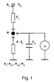
- Such a measuring arrangement with n antennas A 1 -A n and the network N to be measured is shown schematically in FIG. 1.
- a complex input voltage U 0 is applied to one of the antennas A i , and the other antennas A 1 -A i-1 and A i + 1 -A n are connected to ground.
- the complex input voltage U 0 U 0R + iU 0I is made up of a constant DC voltage component and an AC voltage component with a certain frequency 2 ⁇ composed.
- This input voltage U 0 is applied to one of the antennas, the measured value U i being tapped at the network N each time.
- the set of measured values U 1 -U n forms a data field, the values of which represent a "fingerprint" typical of the network N. This measuring method is called field measurement.
- the data fields of the individual networks usually differ. However, if the data fields of two networks are the same, this is usually due to a short circuit between these two networks. This can be checked with a conventional short-circuit test, in which the electrical resistance between these two networks is measured. These short-circuit tests only have to be carried out on networks with identical data fields, so that the measurement effort is very low compared to similar measurement methods.
- the interruption can be checked in a known manner by measuring the resistance, in which electrodes tap the resistance at the ends of the network, or by comparing the data field with a reference field.
- the invention has for its object to provide a simple and quick method for testing an electrical conductor arrangement and an apparatus for performing this method.
- the object is achieved by a method having the features of claim 1, 13, 15 and by a device having the features of claim 19.
- a first conductor arrangement is measured in a first measuring process by means of a field measurement to determine short circuits between individual networks and by means of a resistance measurement to determine interruptions in the individual networks. From the data fields determined in this way, conductance values between the individual networks and the corresponding antennas are determined and stored as reference conductance values.
- a measurement of the complex conductance between each network to be measured and a single antenna is carried out to determine short circuits, the complex actual conductance ascertained being compared with the corresponding reference conductance.
- the comparison between the conductance value and the reference conductance value can be used to determine the interruptions, high-impedance short circuits between the networks and interruptions in the networks being able to be detected by taking into account the real part of the actual conductance value.
- the method according to the invention is divided into a first measuring process for testing a first conductor arrangement and subsequent measuring processes for testing a further conductor arrangement.
- the first measurement process comprises a field measurement to determine the short circuits between networks and a resistance measurement to determine interruptions.
- a measuring arrangement for field measurement is shown schematically.
- This measuring arrangement has n antennas A 1 -A n with which a network N is measured.
- a complex input voltage U 0 is applied to one of the antennas A i
- the other antennas A 1 -A i-1 and A i + 1 -A n are connected to ground.
- FIG. 2 schematically shows a section of a conductor arrangement, four networks being used as antennas A 1 -A 4 for testing the other networks N 1 -N 4 .
- external antennas can also be used.
- This input voltage U 0 is applied to one of the antennas A i , each time a voltage U i is tapped as a measured value from the network N.
- the voltage U i is the potential of the electrical field between the antenna A, to which the input voltage U 0 is applied, and the antennas connected to ground. An electrical field is thus tapped with this voltage measurement, which is why this method is referred to as field measurement.
- the set of measured values U 1 to U n forms the data field which is characteristic of the network N.
- the data fields of the individual networks N i generally differ. If the data fields of two networks match, this is mostly due to a short circuit between these two networks. This can be checked with a conventional short-circuit test, in which the resistance between these two networks is measured. These short-circuit tests are only carried out on networks with identical or similar data fields within certain limits, so that the measurement effort is very low compared to conventional measurement methods.
- the interruption check is carried out by means of a resistance measurement, in which electrodes at the ends of the network tap the resistance.
- the combined measurement procedure with field and resistance measurement in the first measurement process makes you independent of a "golden board” or prepared reference data.
- Y I. ⁇ U iR ⁇ ( U 0 - ⁇ U iR ) - ( ⁇ U iI ) 2nd ( U 0 - ⁇ U iR ) 2nd + ( ⁇ U iI ) 2nd ⁇ ⁇ ⁇ C. p (5)
- Y R - U 0 ⁇ ⁇ U iI ( U 0 - ⁇ U iR ) 2nd + ( ⁇ U iI ) 2nd ⁇ ⁇ ⁇ C. p
- the sum symbols each represent a sum of 1 to n of a data field of a network.
- the conductance values can be determined from the data obtained with the field measurement with an accuracy of better than 1.5%, so that they are suitable as reference values for a measurement method working with a conductance comparison.
- the complex conductance values Y i between the networks and the antennas A i are therefore calculated simultaneously with the testing of a conductor arrangement.
- the guide values Y i and the capacitances C ia are stored as reference values for the subsequent measurement processes.
- a i consists of calculating from the field data. This is expedient if an antenna is used in the further measuring processes, which consists of several antennas A i which are electrically short-circuited to one another. It is also possible to save the data fields of the field measurement and to calculate the corresponding capacitances with each further measurement process, so that the arrangement of the antennas can be varied.
- the further measurement processes are carried out by measuring the conductance of the conductance values Y k between the networks N k and one of the antennas A i . These actual guide values Y k are compared with the corresponding reference values, and in the event of deviations it is examined whether there is a short circuit with another network or an interruption in the network or both.
- a short circuit can be determined similarly to the impedance comparison known from the prior art (e.g. DE 34 08 704 A1 or EP 0 438 491 B1).
- the capacitance or the impedance of the network is measured here, and if there are deviations from the reference value, a conventional resistance measurement is carried out in order to localize the short circuit.
- a disadvantage of these known methods working with an impedance comparison is that high-resistance short circuits cannot be determined from the impedance comparison. These high-resistance short-circuits can therefore only be determined with a visual inspection of the conductor arrangement, which is after one a measurement method based on an impedance comparison is absolutely necessary.
- the invention therefore preferably provides a modified comparison of the measured conductance Y i with the reference values for the determination of short circuits for the subsequent further measurement processes.
- a simple and quickly executable measurement of the conductance Y k is provided in order to determine short circuits on the networks N k , the conductance Y k being the conductance between the network N k and the respective antenna A i .
- the measurement effort is significantly reduced since no multiple scanning of a network N k by several antennas A i is necessary.
- the further measuring processes for determining short circuits between the individual networks N k are thus based on the measurement of the conductance Y k , which can be carried out simply and quickly, and high-resistance short circuits can also be determined. If a short circuit is found on a network, it is localized in a known manner with a resistance measurement.
- the values ⁇ Y and ⁇ C are empirical values that depend on the measuring device used and the type of the conductor arrangement.
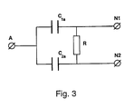
- condition C 2a ⁇ C 1a can be met simply by exchanging the corresponding networks N.
- Interruptions in the networks N k can occur in the further measuring processes either by a resistance measurement known per se or by comparing the actual conductance Y k or the actual capacitance C k with the stored reference values.
- the minimum capacitance is about 1nF.
- Such capacities are generally achieved by larger track layouts with a few hundred or more test points.
- the criterion is whether there is an interruption: ⁇ * C. - Y 1 I. + ⁇ Y + ⁇ C. ⁇ ⁇ ⁇ C. 4th and Y 1 R + ⁇ Y ⁇ R TU ⁇ ⁇ 2nd ⁇ C. 2nd 8th
- the interruption can be localized using a resistance measurement known per se.
- the measured conductance Y k or the measured capacitance C ka is stored as a reference value.
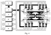
- a device for carrying out the method has a plurality of electrodes 1 which can be contacted with test points 2 of the networks N k on a conductor arrangement 3 (FIGS. 2, 4).
- the electrodes 1 can preferably be used as antenna probes and as measuring probes. As antenna probes, they apply either the input voltage U 0 or ground to the networks connected to them, so that the networks connected to them act as antennas.
- the measuring probe taps off the voltage U i present at the network connected to it.
- a preferred embodiment of the measuring device is a so-called multi-finger system (FIG. 4), in which an electrode 1 is integrated into a measuring finger 4.
- a multi-finger system in which the measuring fingers can be moved independently of one another is described in EP 0 468 153 A1.
- the measuring fingers 4 can be moved parallel to the surface of the conductor arrangement 3, so that the electrodes can be contacted with certain test points 2 of the networks N k .
- Such a multi-finger system has, for example, 16 measuring fingers 4, eight being arranged above and eight below the conductor arrangement 3 in order to contact the conductor arrangement 3 from both sides.
- the measuring fingers 4 are each fastened to a carriage 6 which is controlled by a position control device 5 and which can be moved in one plane parallel to the conductor arrangement 3.
- the carriages 6 are each provided with a vertically aligned actuating cylinder 7 with which the measuring fingers 4 can be rotated about the vertical axis. Furthermore, a tilting device is integrated in the measuring fingers 4 so that the finger can be lowered onto the conductor arrangement 3 with the probe 1 arranged at its tip.
- the conductor arrangement 3 is subdivided into specific segments, with certain networks of this segment being selected as antennas for each segment.
- the networks selected as antennas are each in contact with one of the electrodes 1 during the measurement of this segment, the other electrodes 1 alternately contacting a network of the segment for receiving the measurement voltage U i .
- the network to be measured is simultaneously contacted with another electrode 1 at at least one further test point 2, so that the resistance value of the network between the two electrodes 1 can be tapped.
- the networks are checked for interruptions, whereby all test points on a network are tapped in pairs.
- the position control device 5 receives to control the movement the measuring finger 4 receives its signals from a central control unit 8.
- the central control unit 8 connects an antenna of the segment with a function generator 9, which outputs the measurement voltage U 0 , and the other antennas to ground.
- the central control unit establishes a connection of the network N k to be measured via a single electrode 1 to a first evaluation device 10 for field measurement, the voltage U i being tapped at the network N.
- Further networks N k can be scanned in the area of a segment without the electrodes 1 connected to the antennas being moved, but only the electrodes 1 for contacting the networks to be measured.
- test points 2 of the network N k are each connected in pairs to an electrode 1.
- the resistance value of this network is recorded by a second evaluation device 11 and passed on to the central control unit.
- the electrodes 1 connected to the antennas are not moved, and the other electrodes 1 are contacted with the networks to be measured.
- the first evaluation device 10 picks up the tapped voltages U i (field measurement) and forwards them to the central control unit, which determines and stores the reference guide values.
- the measuring fingers 4 are controlled so that in a segment a single electrode 1 is connected to an antenna or an antenna combination, and the other measuring fingers 4 are connected their electrodes 1 scan the test points 2 to be measured so that the capacitances C k or the imaginary part of the conductance Y kI between the antenna A and the network N k to be measured is recorded at the respective test point 2 with a third evaluation device 12.
- the resistance or the real part Y kR between the antenna A and the network N k to be measured is detected by the second evaluation device 11.
- a probe 1 is thus permanently contacted with an antenna in a further measurement process, and all test points 2 are contacted once with a probe 1 to record the conductance.
- a conductance measurement is first carried out between the antenna A and the network N k , for which purpose a probe 1 is contacted with an antenna and another probe 1 with a test point 2 of the network. To determine interruptions, all test points are contacted in pairs with two probes 1.
- the second and third evaluation devices 11, 12 for sensing resistance or capacitance are based on a current measurement.
- a multi-finger system the central control unit 8 of which is designed to carry out the method according to the invention, has to carry out a much smaller number of movements of the measuring fingers 4 when measuring the same conductor arrangements compared to known multi-finger systems, since short circuits with a single conductance measurement per network, and in the case of larger networks interruptions can be detected with one conductance measurement per test point.
- the improvements achieved by the invention are based, inter alia, on the fact that the guide values and not, as in the prior art, their reciprocal values, the impedances, are examined, as a result of which the information contained therein can be evaluated more effectively.
Landscapes
- Engineering & Computer Science (AREA)
- Computer Hardware Design (AREA)
- Microelectronics & Electronic Packaging (AREA)
- General Engineering & Computer Science (AREA)
- Physics & Mathematics (AREA)
- General Physics & Mathematics (AREA)
- Measurement Of Resistance Or Impedance (AREA)
- Testing Of Short-Circuits, Discontinuities, Leakage, Or Incorrect Line Connections (AREA)
Applications Claiming Priority (2)
| Application Number | Priority Date | Filing Date | Title |
|---|---|---|---|
| DE19541307 | 1995-11-06 | ||
| DE19541307A DE19541307C2 (de) | 1995-11-06 | 1995-11-06 | Verfahren zum Prüfen von elektrischen Leiteranordnungen und Vorrichtung zum Ausführen des Verfahrens |
Publications (3)
| Publication Number | Publication Date |
|---|---|
| EP0772054A2 true EP0772054A2 (fr) | 1997-05-07 |
| EP0772054A3 EP0772054A3 (fr) | 1998-02-25 |
| EP0772054B1 EP0772054B1 (fr) | 2003-04-23 |
Family
ID=7776743
Family Applications (1)
| Application Number | Title | Priority Date | Filing Date |
|---|---|---|---|
| EP96117642A Expired - Lifetime EP0772054B1 (fr) | 1995-11-06 | 1996-11-04 | Procédé et appareil pour tester des structures de conducteur |
Country Status (4)
| Country | Link |
|---|---|
| US (1) | US5903160A (fr) |
| EP (1) | EP0772054B1 (fr) |
| JP (1) | JP3183195B2 (fr) |
| DE (2) | DE19541307C2 (fr) |
Cited By (5)
| Publication number | Priority date | Publication date | Assignee | Title |
|---|---|---|---|---|
| EP0919820A3 (fr) * | 1997-10-30 | 2000-02-02 | Nidec-Read Corporation | Appareil et méthode de test de carte à circuits |
| DE10260238A1 (de) * | 2002-12-20 | 2004-07-22 | Atg Test Systems Gmbh & Co.Kg | Adapter zum Testen von Leiterplatten |
| WO2006133808A1 (fr) | 2005-06-17 | 2006-12-21 | Atg Test Systems Gmbh | Procede pour tester des cartes de circuits imprimes de grandes surfaces non equipees, au moyen d'un testeur a pattes |
| WO2010043651A3 (fr) * | 2008-10-15 | 2010-06-17 | Dtg International Gmbh | Détermination des propriétés d'un dispositif électrique |
| DE202014105674U1 (de) | 2014-11-25 | 2016-02-26 | MR Electronics Ltd. Niederlassung Deutschland | Kontaktiervorrichtung für Platinen |
Families Citing this family (8)
| Publication number | Priority date | Publication date | Assignee | Title |
|---|---|---|---|---|
| DE19541307C2 (de) * | 1995-11-06 | 2001-09-27 | Atg Test Systems Gmbh | Verfahren zum Prüfen von elektrischen Leiteranordnungen und Vorrichtung zum Ausführen des Verfahrens |
| DE19610556A1 (de) * | 1996-03-18 | 1997-09-25 | Siemens Ag | Bussegment beziehungsweise Busanschaltung zum Anschließen einer Baugruppe einer speicherprogrammierbaren Steuerung an einen Bus |
| DE10025751A1 (de) * | 2000-05-24 | 2001-12-06 | Atg Test Systems Gmbh | Verfahren zum Untersuchen einer leiterplatte an einem vorbestimmten Bereich der Leiterplatte und Vorrichtung zum Durchführen des Verfahrens |
| US7030623B1 (en) | 2004-02-03 | 2006-04-18 | Kevin Carpenter | Electrical short tracing apparatus and method |
| US10191108B2 (en) * | 2015-11-19 | 2019-01-29 | Globalfoundries Inc. | On-chip sensor for monitoring active circuits on integrated circuit (IC) chips |
| DE102017102700A1 (de) * | 2017-02-10 | 2018-09-13 | Atg Luther & Maelzer Gmbh | Prüfvorrichtung und Verfahren zum Prüfen von Leiterplatten |
| JP6386606B1 (ja) * | 2017-02-27 | 2018-09-05 | ファナック株式会社 | 接続機器の接続回路 |
| JP7227017B2 (ja) * | 2019-01-29 | 2023-02-21 | 北陸電力株式会社 | 避雷装置の故障判定方法および避雷装置の故障判定装置 |
Citations (4)
| Publication number | Priority date | Publication date | Assignee | Title |
|---|---|---|---|---|
| US3975680A (en) | 1975-06-25 | 1976-08-17 | Honeywell Information Systems, Inc. | Non-contact coupling plate for circuit board tester |
| DE3408704A1 (de) | 1983-03-07 | 1984-09-13 | Kollmorgen Technologies Corp., Dallas, Tex. | Verfahren und vorrichtung zum pruefen von verbindungsnetzwerk-schaltungen |
| EP0438491B1 (fr) | 1988-10-17 | 1994-07-20 | Bath Scientific Limited | Procede permettant de tester les circuits electriques |
| EP0508062B1 (fr) | 1991-04-10 | 1995-07-19 | atg test systems GmbH | Méthode et dispositif pour tester un arrangement de conducteurs électriques |
Family Cites Families (11)
| Publication number | Priority date | Publication date | Assignee | Title |
|---|---|---|---|---|
| DE2311903A1 (de) * | 1973-03-09 | 1974-09-12 | Siemens Ag | Verfahren und einrichtung zur ortung von kurzschluessen in mehrlagenverdrahtungen |
| US4528500A (en) * | 1980-11-25 | 1985-07-09 | Lightbody James D | Apparatus and method for testing circuit boards |
| EP0246034A3 (fr) * | 1986-05-16 | 1989-04-05 | AT&T Corp. | Test de dispositifs électroniques pendant leur fabrication |
| JPH0246034A (ja) * | 1988-08-06 | 1990-02-15 | Mitsubishi Electric Corp | データ多重化装置 |
| CA2049616C (fr) * | 1991-01-22 | 2000-04-04 | Jacob Soiferman | Methode de verification sans contact et systeme de verification de cartes de circuits integres |
| US5424633A (en) * | 1991-01-22 | 1995-06-13 | Advanced Test Technologies Inc. | Contactless test method and system for testing printed circuit boards |
| DE4134193A1 (de) * | 1991-04-10 | 1992-10-15 | Atg Electronic Gmbh | Verfahren und vorrichtung zur pruefung einer elektrischen leiteranordnung |
| EP0527321A1 (fr) * | 1991-08-05 | 1993-02-17 | Siemens Aktiengesellschaft | Méthode de diagnostic automatique de défauts de circuits électriques |
| US5631572A (en) * | 1993-09-17 | 1997-05-20 | Teradyne, Inc. | Printed circuit board tester using magnetic induction |
| DE69517453T2 (de) * | 1994-01-12 | 2001-02-08 | Advantest Corp., Tokio/Tokyo | Berührungslose-Beobachtungsvorrichtung von Wellensignalen |
| DE19541307C2 (de) * | 1995-11-06 | 2001-09-27 | Atg Test Systems Gmbh | Verfahren zum Prüfen von elektrischen Leiteranordnungen und Vorrichtung zum Ausführen des Verfahrens |
-
1995
- 1995-11-06 DE DE19541307A patent/DE19541307C2/de not_active Expired - Lifetime
-
1996
- 1996-11-04 EP EP96117642A patent/EP0772054B1/fr not_active Expired - Lifetime
- 1996-11-04 DE DE59610371T patent/DE59610371D1/de not_active Expired - Lifetime
- 1996-11-05 US US08/743,196 patent/US5903160A/en not_active Expired - Lifetime
- 1996-11-06 JP JP29383396A patent/JP3183195B2/ja not_active Expired - Lifetime
Patent Citations (4)
| Publication number | Priority date | Publication date | Assignee | Title |
|---|---|---|---|---|
| US3975680A (en) | 1975-06-25 | 1976-08-17 | Honeywell Information Systems, Inc. | Non-contact coupling plate for circuit board tester |
| DE3408704A1 (de) | 1983-03-07 | 1984-09-13 | Kollmorgen Technologies Corp., Dallas, Tex. | Verfahren und vorrichtung zum pruefen von verbindungsnetzwerk-schaltungen |
| EP0438491B1 (fr) | 1988-10-17 | 1994-07-20 | Bath Scientific Limited | Procede permettant de tester les circuits electriques |
| EP0508062B1 (fr) | 1991-04-10 | 1995-07-19 | atg test systems GmbH | Méthode et dispositif pour tester un arrangement de conducteurs électriques |
Cited By (12)
| Publication number | Priority date | Publication date | Assignee | Title |
|---|---|---|---|---|
| EP0919820A3 (fr) * | 1997-10-30 | 2000-02-02 | Nidec-Read Corporation | Appareil et méthode de test de carte à circuits |
| DE10260238A1 (de) * | 2002-12-20 | 2004-07-22 | Atg Test Systems Gmbh & Co.Kg | Adapter zum Testen von Leiterplatten |
| DE10260238B4 (de) * | 2002-12-20 | 2007-04-05 | Atg Test Systems Gmbh & Co.Kg | Adapter zum Testen einer oder mehrerer Leiteranordnungen und Verfahren |
| WO2006133808A1 (fr) | 2005-06-17 | 2006-12-21 | Atg Test Systems Gmbh | Procede pour tester des cartes de circuits imprimes de grandes surfaces non equipees, au moyen d'un testeur a pattes |
| DE102005028191A1 (de) * | 2005-06-17 | 2006-12-28 | Atg Test Systems Gmbh & Co. Kg Reicholzheim | Verfahren zum Testen von unbestückten, großflächigen Leiterplatten mit einem Fingertester |
| DE102005028191B4 (de) * | 2005-06-17 | 2009-04-09 | Atg Luther & Maelzer Gmbh | Verfahren und Vorrichtung zum Testen von unbestückten, großflächigen Leiterplatten mit einem Fingertester |
| WO2010043651A3 (fr) * | 2008-10-15 | 2010-06-17 | Dtg International Gmbh | Détermination des propriétés d'un dispositif électrique |
| CN102187239A (zh) * | 2008-10-15 | 2011-09-14 | Dtg国际有限公司 | 电气设备特性的确定 |
| US8704545B2 (en) | 2008-10-15 | 2014-04-22 | Dtg International Gmbh | Determination of properties of an electrical device |
| TWI461711B (zh) * | 2008-10-15 | 2014-11-21 | Dtg Int Gmbh | 決定電裝置特性之裝置與方法 |
| CN102187239B (zh) * | 2008-10-15 | 2015-07-22 | Dtg国际有限公司 | 电气设备特性的确定 |
| DE202014105674U1 (de) | 2014-11-25 | 2016-02-26 | MR Electronics Ltd. Niederlassung Deutschland | Kontaktiervorrichtung für Platinen |
Also Published As
| Publication number | Publication date |
|---|---|
| US5903160A (en) | 1999-05-11 |
| DE19541307A1 (de) | 1997-05-15 |
| JPH09178798A (ja) | 1997-07-11 |
| EP0772054A3 (fr) | 1998-02-25 |
| EP0772054B1 (fr) | 2003-04-23 |
| DE19541307C2 (de) | 2001-09-27 |
| DE59610371D1 (de) | 2003-05-28 |
| JP3183195B2 (ja) | 2001-07-03 |
Similar Documents
| Publication | Publication Date | Title |
|---|---|---|
| DE3408704C2 (de) | Verfahren zum Prüfen von starren oder flexiblen elektrischen Verbindungsnetzwerk-Schaltungen und Vorrichtung zur Durchführung des Verfahrens | |
| DE4026295C2 (fr) | ||
| EP0508062B1 (fr) | Méthode et dispositif pour tester un arrangement de conducteurs électriques | |
| EP0285799B1 (fr) | Dispositif de test électrique du fonctionnement de rangées de fils électriques, en particulier pour cartes de circuit | |
| DE102007046054B4 (de) | Verbesserter hochgenauer Rogowski-Stromwandler | |
| DE69432829T2 (de) | Kabelidentifizierungsgerät zum Prüfen von Kabeln in lokalen Netzen | |
| EP0772054B1 (fr) | Procédé et appareil pour tester des structures de conducteur | |
| EP0853242B1 (fr) | Procédé pour tester des cartes de circuits imprimés | |
| DE102013005939A1 (de) | Messwiderstand und entsprechendes Messverfahren | |
| DE2744299C2 (de) | Verfahren zum elektrischen Prüfen eines Leiterbahnmusters auf einem Substrat | |
| DE4317285A1 (de) | Kapazitive Meßsonde für die Bestimmung von Werkstückabmessungen | |
| DE68914005T2 (de) | Leitende Muster für den elektrischen Test von Halbleiterbausteinen. | |
| DE2701857C2 (fr) | ||
| DE68916969T2 (de) | Prüfung von elektrischen kreisen. | |
| EP1151310B1 (fr) | Procede de mesure pour systeme de mesure capacitif | |
| WO2021209309A1 (fr) | Dispositif de test, système d'appareil de commande et procédé de test | |
| EP1920263B1 (fr) | Procede pour tester des cartes de circuits imprimes de grandes surfaces non equipees, au moyen d'un testeur a pattes | |
| DE4406674A1 (de) | Verfahren zum Prüfen einer zu prüfenden Elektrodenplatte | |
| DE4234548C1 (de) | Anordnung zum Erfassen von Verkehrsgrößen | |
| EP3764054B1 (fr) | Agencement de capteur permettant de détecter une déviation d'une fil électrode | |
| DE112018004610T5 (de) | Kapazitives Sensorsystem | |
| DE4312862A1 (de) | Drehbarer Kapazitanzsensor | |
| DE202013103151U1 (de) | Vorrichtung zur zerstörungsfreien Wirbelstromprüfung eines Bauteils | |
| DE4134193A1 (de) | Verfahren und vorrichtung zur pruefung einer elektrischen leiteranordnung | |
| DE102024110653B3 (de) | Messsystem und Verfahren zur Charakterisierung einer mehrschichtigen Struktur mit schichtweise unterschiedlichen ohmschen Eigenschaften, Sensormodul für ein Messsystem, Fertigungsanlage für eine mehrschichtige Struktur mit schichtweise unterschiedlichen ohmschen Eigenschaften |
Legal Events
| Date | Code | Title | Description |
|---|---|---|---|
| PUAI | Public reference made under article 153(3) epc to a published international application that has entered the european phase |
Free format text: ORIGINAL CODE: 0009012 |
|
| 17P | Request for examination filed |
Effective date: 19961104 |
|
| AK | Designated contracting states |
Kind code of ref document: A2 Designated state(s): DE FR GB IT |
|
| PUAL | Search report despatched |
Free format text: ORIGINAL CODE: 0009013 |
|
| AK | Designated contracting states |
Kind code of ref document: A3 Designated state(s): DE FR GB IT |
|
| RAP1 | Party data changed (applicant data changed or rights of an application transferred) |
Owner name: ATG TEST SYSTEMS GMBH & CO. KG |
|
| 17Q | First examination report despatched |
Effective date: 20020204 |
|
| GRAH | Despatch of communication of intention to grant a patent |
Free format text: ORIGINAL CODE: EPIDOS IGRA |
|
| GRAH | Despatch of communication of intention to grant a patent |
Free format text: ORIGINAL CODE: EPIDOS IGRA |
|
| GRAA | (expected) grant |
Free format text: ORIGINAL CODE: 0009210 |
|
| AK | Designated contracting states |
Designated state(s): DE FR GB IT |
|
| REG | Reference to a national code |
Ref country code: GB Ref legal event code: FG4D Free format text: NOT ENGLISH |
|
| GBT | Gb: translation of ep patent filed (gb section 77(6)(a)/1977) |
Effective date: 20030423 |
|
| REF | Corresponds to: |
Ref document number: 59610371 Country of ref document: DE Date of ref document: 20030528 Kind code of ref document: P |
|
| ET | Fr: translation filed | ||
| PLBE | No opposition filed within time limit |
Free format text: ORIGINAL CODE: 0009261 |
|
| STAA | Information on the status of an ep patent application or granted ep patent |
Free format text: STATUS: NO OPPOSITION FILED WITHIN TIME LIMIT |
|
| 26N | No opposition filed |
Effective date: 20040126 |
|
| REG | Reference to a national code |
Ref country code: DE Ref legal event code: R082 Ref document number: 59610371 Country of ref document: DE Representative=s name: PATRONUS IP PATENT- & RECHTSANWAELTE BERNHARD , DE |
|
| REG | Reference to a national code |
Ref country code: FR Ref legal event code: PLFP Year of fee payment: 20 |
|
| PGFP | Annual fee paid to national office [announced via postgrant information from national office to epo] |
Ref country code: GB Payment date: 20151123 Year of fee payment: 20 Ref country code: DE Payment date: 20151120 Year of fee payment: 20 |
|
| PGFP | Annual fee paid to national office [announced via postgrant information from national office to epo] |
Ref country code: FR Payment date: 20151123 Year of fee payment: 20 |
|
| PGFP | Annual fee paid to national office [announced via postgrant information from national office to epo] |
Ref country code: IT Payment date: 20151130 Year of fee payment: 20 |
|
| REG | Reference to a national code |
Ref country code: DE Ref legal event code: R071 Ref document number: 59610371 Country of ref document: DE |
|
| REG | Reference to a national code |
Ref country code: GB Ref legal event code: PE20 Expiry date: 20161103 |
|
| PG25 | Lapsed in a contracting state [announced via postgrant information from national office to epo] |
Ref country code: GB Free format text: LAPSE BECAUSE OF EXPIRATION OF PROTECTION Effective date: 20161103 |