EP0772071B1 - Elément d'affichage à cristal liquide et son procédé de fabrication - Google Patents
Elément d'affichage à cristal liquide et son procédé de fabrication Download PDFInfo
- Publication number
- EP0772071B1 EP0772071B1 EP96308051A EP96308051A EP0772071B1 EP 0772071 B1 EP0772071 B1 EP 0772071B1 EP 96308051 A EP96308051 A EP 96308051A EP 96308051 A EP96308051 A EP 96308051A EP 0772071 B1 EP0772071 B1 EP 0772071B1
- Authority
- EP
- European Patent Office
- Prior art keywords
- liquid crystal
- spacer
- crystal display
- display element
- alignment
- Prior art date
- Legal status (The legal status is an assumption and is not a legal conclusion. Google has not performed a legal analysis and makes no representation as to the accuracy of the status listed.)
- Expired - Lifetime
Links
- 239000004973 liquid crystal related substance Substances 0.000 title claims description 71
- 238000000034 method Methods 0.000 title claims description 68
- 230000008569 process Effects 0.000 title claims description 44
- 238000004519 manufacturing process Methods 0.000 title claims description 15
- 239000000758 substrate Substances 0.000 claims description 83
- 125000006850 spacer group Chemical group 0.000 claims description 74
- 239000000463 material Substances 0.000 claims description 32
- 229920005989 resin Polymers 0.000 claims description 11
- 239000011347 resin Substances 0.000 claims description 11
- 239000005262 ferroelectric liquid crystals (FLCs) Substances 0.000 claims description 10
- 229910052751 metal Inorganic materials 0.000 claims description 5
- 239000002184 metal Substances 0.000 claims description 5
- 229920002120 photoresistant polymer Polymers 0.000 claims description 5
- 238000010276 construction Methods 0.000 description 7
- VYPSYNLAJGMNEJ-UHFFFAOYSA-N Silicium dioxide Chemical compound O=[Si]=O VYPSYNLAJGMNEJ-UHFFFAOYSA-N 0.000 description 6
- 239000000853 adhesive Substances 0.000 description 6
- 230000001070 adhesive effect Effects 0.000 description 6
- 230000002411 adverse Effects 0.000 description 6
- 230000000694 effects Effects 0.000 description 6
- 230000035939 shock Effects 0.000 description 6
- 238000004528 spin coating Methods 0.000 description 6
- 239000004642 Polyimide Substances 0.000 description 5
- 239000010419 fine particle Substances 0.000 description 5
- 238000000206 photolithography Methods 0.000 description 5
- 229920001721 polyimide Polymers 0.000 description 5
- 230000015572 biosynthetic process Effects 0.000 description 4
- 229910052681 coesite Inorganic materials 0.000 description 3
- 229910052906 cristobalite Inorganic materials 0.000 description 3
- 150000002739 metals Chemical class 0.000 description 3
- 229910052750 molybdenum Inorganic materials 0.000 description 3
- 239000004033 plastic Substances 0.000 description 3
- 239000000377 silicon dioxide Substances 0.000 description 3
- 229910052682 stishovite Inorganic materials 0.000 description 3
- 229910052905 tridymite Inorganic materials 0.000 description 3
- IJGRMHOSHXDMSA-UHFFFAOYSA-N Atomic nitrogen Chemical compound N#N IJGRMHOSHXDMSA-UHFFFAOYSA-N 0.000 description 2
- -1 acryl Chemical group 0.000 description 2
- 229910052782 aluminium Inorganic materials 0.000 description 2
- 230000015556 catabolic process Effects 0.000 description 2
- 229910052804 chromium Inorganic materials 0.000 description 2
- 238000006731 degradation reaction Methods 0.000 description 2
- 230000006866 deterioration Effects 0.000 description 2
- 239000011521 glass Substances 0.000 description 2
- 230000004048 modification Effects 0.000 description 2
- 238000012986 modification Methods 0.000 description 2
- 230000004044 response Effects 0.000 description 2
- 239000002904 solvent Substances 0.000 description 2
- 238000004544 sputter deposition Methods 0.000 description 2
- MYRTYDVEIRVNKP-UHFFFAOYSA-N 1,2-Divinylbenzene Chemical class C=CC1=CC=CC=C1C=C MYRTYDVEIRVNKP-UHFFFAOYSA-N 0.000 description 1
- LFQSCWFLJHTTHZ-UHFFFAOYSA-N Ethanol Chemical compound CCO LFQSCWFLJHTTHZ-UHFFFAOYSA-N 0.000 description 1
- 101000635799 Homo sapiens Run domain Beclin-1-interacting and cysteine-rich domain-containing protein Proteins 0.000 description 1
- ZOKXTWBITQBERF-UHFFFAOYSA-N Molybdenum Chemical compound [Mo] ZOKXTWBITQBERF-UHFFFAOYSA-N 0.000 description 1
- 102100030852 Run domain Beclin-1-interacting and cysteine-rich domain-containing protein Human genes 0.000 description 1
- 230000001112 coagulating effect Effects 0.000 description 1
- 230000000052 comparative effect Effects 0.000 description 1
- 238000011109 contamination Methods 0.000 description 1
- 239000013078 crystal Substances 0.000 description 1
- 230000007547 defect Effects 0.000 description 1
- 239000007789 gas Substances 0.000 description 1
- AMGQUBHHOARCQH-UHFFFAOYSA-N indium;oxotin Chemical compound [In].[Sn]=O AMGQUBHHOARCQH-UHFFFAOYSA-N 0.000 description 1
- 229910010272 inorganic material Inorganic materials 0.000 description 1
- 239000011147 inorganic material Substances 0.000 description 1
- 239000011159 matrix material Substances 0.000 description 1
- 239000003595 mist Substances 0.000 description 1
- 239000011733 molybdenum Substances 0.000 description 1
- 229910052757 nitrogen Inorganic materials 0.000 description 1
- 239000011368 organic material Substances 0.000 description 1
- 239000002245 particle Substances 0.000 description 1
- 230000010287 polarization Effects 0.000 description 1
- 229920000642 polymer Polymers 0.000 description 1
- 238000007789 sealing Methods 0.000 description 1
- 239000012798 spherical particle Substances 0.000 description 1
- 230000002269 spontaneous effect Effects 0.000 description 1
- 239000007921 spray Substances 0.000 description 1
- 238000005507 spraying Methods 0.000 description 1
- 239000012780 transparent material Substances 0.000 description 1
Images


Classifications
-
- G—PHYSICS
- G02—OPTICS
- G02F—OPTICAL DEVICES OR ARRANGEMENTS FOR THE CONTROL OF LIGHT BY MODIFICATION OF THE OPTICAL PROPERTIES OF THE MEDIA OF THE ELEMENTS INVOLVED THEREIN; NON-LINEAR OPTICS; FREQUENCY-CHANGING OF LIGHT; OPTICAL LOGIC ELEMENTS; OPTICAL ANALOGUE/DIGITAL CONVERTERS
- G02F1/00—Devices or arrangements for the control of the intensity, colour, phase, polarisation or direction of light arriving from an independent light source, e.g. switching, gating or modulating; Non-linear optics
- G02F1/01—Devices or arrangements for the control of the intensity, colour, phase, polarisation or direction of light arriving from an independent light source, e.g. switching, gating or modulating; Non-linear optics for the control of the intensity, phase, polarisation or colour
- G02F1/13—Devices or arrangements for the control of the intensity, colour, phase, polarisation or direction of light arriving from an independent light source, e.g. switching, gating or modulating; Non-linear optics for the control of the intensity, phase, polarisation or colour based on liquid crystals, e.g. single liquid crystal display cells
- G02F1/133—Constructional arrangements; Operation of liquid crystal cells; Circuit arrangements
- G02F1/1333—Constructional arrangements; Manufacturing methods
- G02F1/1339—Gaskets; Spacers; Sealing of cells
- G02F1/13394—Gaskets; Spacers; Sealing of cells spacers regularly patterned on the cell subtrate, e.g. walls, pillars
-
- G—PHYSICS
- G02—OPTICS
- G02F—OPTICAL DEVICES OR ARRANGEMENTS FOR THE CONTROL OF LIGHT BY MODIFICATION OF THE OPTICAL PROPERTIES OF THE MEDIA OF THE ELEMENTS INVOLVED THEREIN; NON-LINEAR OPTICS; FREQUENCY-CHANGING OF LIGHT; OPTICAL LOGIC ELEMENTS; OPTICAL ANALOGUE/DIGITAL CONVERTERS
- G02F1/00—Devices or arrangements for the control of the intensity, colour, phase, polarisation or direction of light arriving from an independent light source, e.g. switching, gating or modulating; Non-linear optics
- G02F1/01—Devices or arrangements for the control of the intensity, colour, phase, polarisation or direction of light arriving from an independent light source, e.g. switching, gating or modulating; Non-linear optics for the control of the intensity, phase, polarisation or colour
- G02F1/13—Devices or arrangements for the control of the intensity, colour, phase, polarisation or direction of light arriving from an independent light source, e.g. switching, gating or modulating; Non-linear optics for the control of the intensity, phase, polarisation or colour based on liquid crystals, e.g. single liquid crystal display cells
- G02F1/133—Constructional arrangements; Operation of liquid crystal cells; Circuit arrangements
- G02F1/1333—Constructional arrangements; Manufacturing methods
- G02F1/1337—Surface-induced orientation of the liquid crystal molecules, e.g. by alignment layers
- G02F1/133711—Surface-induced orientation of the liquid crystal molecules, e.g. by alignment layers by organic films, e.g. polymeric films
Definitions
- the method (1) include a dry method in which spherical fine particles, made of, for example, an organic resin, such as a polymer of divinylbenzenes, are dispersed in a gas flow of nitrogen and then sprayed on the substrates, and a method in which the spherical fine particles are mixed in an alcohol solution or other solutions and sprayed on the substrates in a mist state.
- spherical fine particles made of, for example, an organic resin, such as a polymer of divinylbenzenes
- method (1) has the following problems:
- the first problem is that since the fine particles have a coagulating property whereby they coagulate with one another, it is difficult to spray them on the substrates in a uniform manner and consequently to achieve a uniform cell thickness.
- the second problem is that since it is difficult to control the adherence location of the fine particles, the particles, which have been unintentionally sprayed on pixels, tend to cause defects in the orientation, resulting in low display quality.
- the third problem is that since the substrates are supported by the spherical fine particles that function as spacers only at their contact points, it is difficult to obtain sufficient strength against external pressure.
- ferroelectric liquid crystal has been taken notice of as a prospective liquid crystal material since it has superior properties, such as having spontaneous polarization and providing high-speed response.
- the disadvantage of ferroelectric liquid crystal is that since it has a structure whose molecule-regularity is closer to that of a crystal, once the molecular orientation has been disturbed, it is difficult to return to its original state, that is, it is susceptible to shock.
- method (2) is considered to be a more prospective candidate than method (1).
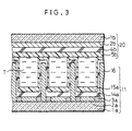
- the substrate 10 is constituted by an insulating substrate 1a, a plurality of electrodes 2a that are placed in parallel with one another, light-shielding films 3a, an insulating film 4a that is formed in a manner so as to cover the insulating substrate 1a, the electrodes 2a and the light-shielding films 3a, spacers 6 that are formed on the surface of the insulating film 4a, and an alignment layer 5a that is formed in a manner so as to cover the surfaces of the insulating film 4a and the spacers 6.
- the substrate 20 is constituted by an insulating substrate 1b, a plurality of electrodes 2b that are placed in parallel with one another, an insulating film 4b, and an alignment layer 5b that is formed on the surface of the insulating layer 4b.
- the insulating substrates 1a and 1b are made of a transparent material such as glass or plastic. Further, transparent electrodes made of ITO (Indium Tin Oxide) are generally used as the electrodes 2a and 2b. However, the electrodes may be constituted by using other metals. Moreover, the light-shielding films 3a are made of metals, such as Cr, Mo and Al, opaque organic resins or other materials.
- ITO Indium Tin Oxide
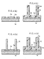
- an ITO film with a film thickness of approximately 100 nm is formed on the insulating substrate 1a by the sputtering method, and this film is patterned by the photolithography so as to form electrodes 2a.
- the resulting shape is shown in Fig. 2(b), wherein the light-shielding films 3a are placed along both sides of each electrode 2a.
- the substrate 10 is manufactured by the above-mentioned processes. Further, the substrate 20 is manufactured as follows: electrodes 2b, light-shielding films, not shown, and an insulating film 4b are successively formed on an insulating substrate 1b through the same processes as described above, and an alignment layer 5b is formed on the insulating film 4b.
- the substrates 10 and 20 are aligned face to face with each other so that their alignment layers 5a and 5b have the same rubbing directions, and the alignment layers films 5a and 5b are bonded to each other by applying a pressure of 0.6 kg/cm 2 at approximately 200°C for one hour. Further, liquid crystal 7 is sealed in the gap between the substrates 10 and 20; thus, a liquid crystal display element is formed.
- the liquid crystal display element manufactured by the above-mentioned processes, is allowed to have a uniform cell thickness with a precision within ⁇ 0.3 ⁇ m. Further, since the vicinity of the spacers 6 is shielded by the light-shielding films 3a and light-shielding films (not shown) on the substrate 20, uniform orientation and switching characteristics are obtained in the pixel display sections.
- the above description exemplifies an arrangement wherein the spacers 6 are formed only on the substrate 10; however, necessary spacers 6 may be formed on the respective substrates 10 and 20 in a separated manner, and the substrates 10 and 20 may be bonded to each other by allowing the alignment layer formed on the spacers 6 on one of the substrates 10 and 20 to adhere to the alignment layer located at regions without spacers on the other substrate.
- the insulating films 4a and 4b are not necessarily required, and they can be omitted as long as no leakage current appears between the substrates 10 and 20. Furthermore, in addition to the above-mentioned various films, an overcoat film and other films may be formed on demand.
- the substrates 10 and 20 are bonded to each other by allowing the alignment layers 5a and 5b, both made of the same material, to be softened and to adhere to each other by applying heat and pressure.
- the spacers 6 are not softened even in this heat and pressure applying process; therefore, different from conventional arrangements, it is possible to prevent the substrate gap from becoming ununiform due to softening and deformation of the spacers, and consequently to control the gap between the substrates 10 and 20 with high precision.
- the paired substrates are bonded to each other by adhesion between the same materials, it is possible to avoid adverse effects, such as deformation or deterioration in one of the materials and insufficient adhesive strength, which tend to occur in adhesion between different materials, such as adhesion between conventional alignment layer and spacers.
- the liquid crystal 7 only contacts the alignment layers 5a and 5b, and is not allowed to contact the spacers 6.
- the orientation and switching characteristics of the liquid crystal tend to become ununiform due to the spacers, resulting in nonuniformity in display.
- the liquid crystal 7 since the liquid crystal 7 does not contact the spacers 6, its orientated state and switching characteristics are not adversely affected by the spacers 6; thus, it becomes possible to achieve a good display state without nonuniformity.
- Fig. 3 is a cross-sectional view showing a schematic construction of a liquid crystal display element of another embodiment of the present invention.
- the liquid crystal display element that was described in the aforementioned Embodiment 1 has an arrangement wherein the spacers 6 are formed on the insulating film 4a and the alignment layer 5a is formed in a manner so as to cover the surfaces of the insulating film 4a and the spacers 6.
- the liquid crystal display element of Embodiment 2 has an arrangement wherein a substrate 11, shown in Fig.
- the liquid crystal display element having the above-mentioned arrangement is manufactured by the following processes: First, the electrodes 2a and the light-shielding films 3a are formed on the surface of the insulating substrate 1a through the processes as illustrated in Figs. 2(a) and 2(b) in the aforementioned embodiment 1.
- Fig. 4(a) shows a state at the time when these processes have been completed.
- the substrates 11 and 20 are bonded to each other in the same manner as the aforementioned Embodiment 1, and liquid crystal 7 is sealed into the gap between them; thus, a liquid crystal display element is formed.
- liquid crystal display element which was manufactured by conventional processes is taken as a comparative example, and is compared with the above-mentioned liquid crystal display elements of the present invention.
- the conventional liquid crystal display element has an arrangement wherein after an alignment layer 35a has been formed, spacers 36 are formed on the alignment layer 35a.
- the manufacturing processes of the conventional liquid crystal display element are as follows:
- ITO was formed on an insulating substrate 31a by the sputtering method as a film with a thickness of 100 nm, and this was patterned by the photolithography so as to form transparent electrodes 32a.
- SiO 2 was applied onto the electrodes 32a by the spin coating method so as to form an insulating film 34a.
- polyimide PSI-A-2101, manufactured by Chisso Corporation was applied onto the insulating film 34a so as to have a film thickness of 50 nm, and after this had been subjected to a baking process at approximately 200°C for one hour, an alignment layer 35a was formed.
- photosensitive organic resin (UR-3100 manufactured by Toray Industries Inc.) by the spin coating method.
- the film thickness was adjusted so that it was set to 1.5 ⁇ m after a baking process.
- a photomask had been placed at portions at which no electrodes 2a were formed, this was irradiated with ultraviolet light, and the non-exposed portions were removed. Furthermore, this was subjected to a baking process at approximately 300°C for one hour; thus, spacers 36 were formed.
- the alignment layer 35a was subjected to a rubbing process; thus, a substrate 30 was completed. Further, the substrate 40 was formed by successively forming electrodes 32b, an insulating film 34b and an alignment layer 35b on the insulating substrate 31b in the same manner as described above.
- the substrates 30 and 40 were bonded to each other with the same rubbing directions, and the upper surface of the spacers 36 and the surface of the alignment layer 35b were allowed to adhere each other by applying a pressure of 0.6 kg/cm 2 at approximately 350°C for one hour. Further, liquid crystal 37 was sealed in the gap in between; thus, a liquid crystal display element was formed.
- the present invention is not intended to be limited by the aforementioned Embodiments, and various modifications are available within the scope of the present invention.
- transparent glass or plastic substrates are used as the insulating substrates 1a and 1b; however, any substrates may be adopted as long as at least one substrate has a light-transmitting property.
- the liquid crystal 7 is not intended to be limited to ferroelectric liquid crystal, and various liquid crystal material may be adopted.
Landscapes
- Physics & Mathematics (AREA)
- Nonlinear Science (AREA)
- Mathematical Physics (AREA)
- Chemical & Material Sciences (AREA)
- Crystallography & Structural Chemistry (AREA)
- General Physics & Mathematics (AREA)
- Optics & Photonics (AREA)
- Liquid Crystal (AREA)
Claims (15)
- Elément d'affichage à cristaux liquides comportant :dans lequel l'une des couches d'alignement est formée de façon à recouvrir au moins ladite entretoise ; etdeux substrats (1a, 1b), dont au moins un est doté d'une propriété de transmission de lumière ;du cristal liquide ;des couches d'alignement (5a, 5b) qui sont formées sur les deux substrats (1a, 1b), respectivement; etune entretoise (6) qui est formée sur au moins un des deux substrats (1a, 1b),
les deux couches d'alignement (5a, 5b) sont réalisées à partir de la même matière ;
caractérisé en ce que les couches d'alignement (5a, 5b) sont unies directement l'une à l'autre à l'emplacement de l'entretoise, et en ce que la matière constitutive desdites couches d'alignement est sélectionnée pour être ramollie et pour que les couches adhèrent l'une à l'autre dans des conditions de pression et de chaleur prédéterminées ; et
l'entretoise (6) est réalisée à partir d'une matière qui ne se ramollit pas dans lesdites conditions prédéterminées. - Elément d'affichage à cristaux liquides selon la revendication 1, dans lequel le cristal liquide est du cristal liquide ferroélectrique.
- Elément d'affichage à cristaux liquides selon la revendication 1, dans lequel l'entretoise a la forme d'une paroi.
- Elément d'affichage à cristaux liquides selon la revendication 1, dans lequel l'entretoise a la forme d'une colonne.
- Elément d'affichage à cristaux liquides selon la revendication 1, dans lequel l'entretoise est formée en dehors des régions de pixels.
- Elément d'affichage à cristaux liquides selon la revendication 1, comportant, en outre, des films pare-lumière pour protéger le voisinage de l'entretoise contre la lumière.
- Elément d'affichage à cristaux liquides selon la revendication 1, dans lequel l'entretoise est réalisée en une matière comprenant une résine organique.
- Elément d'affichage à cristaux liquides selon la revendication 1, dans lequel l'entretoise est réalisée en une matière comprenant un photorésist.
- Elément d'affichage à cristaux liquides selon la revendication 1, dans lequel l'entretoise est réalisée en une matière comprenant un métal.
- Elément d'affichage à cristaux liquides selon la revendication 1, dans lequel l'entretoise est dotée d'une propriété pare-lumière.
- Elément d'affichage à cristaux liquides selon la revendication 1, dans lequel l'entretoise est dotée d'une propriété d'isotropie optique.
- Elément d'affichage à cristaux liquides selon la revendication 1, comportant, en outre, un film isolant qui recouvre toute la surface de l'entretoise, dans lequel la couche d'alignement est formée de façon à recouvrir le film isolant.
- Procédé de fabrication d'un élément d'affichage à cristaux liquides, comportant les étapes consistant :caractérisé en ce que les couches d'alignement (5a, 5b) sont unies directement l'une à l'autre à l'emplacement de l'entretoise, la matière constitutive desdites couches d'alignement est sélectionnée pour être ramollie et pour que les couches adhèrent l'une à l'autre dans des conditions de pression et de chaleur prédéterminées ; età former une entretoise (6) sur un premier substrat isolant (1a) ;à former une couche d'alignement (5a) de façon à recouvrir l'entretoise (6) ;à former au moins une couche d'alignement (5b) sur un second substrat isolant (1b) ; etaprès avoir placé les premier et second substrats isolants (1a, 1b) de sorte que les couches d'alignement respectives (5a, 5b) soient tournées l'une vers l'autre, à laisser les couches d'alignement adhérer l'une à l'autre pendant que de la chaleur et de la pression sont appliquées ; etles deux couches d'alignement (5a, 5b) sont réalisées à partir de la même matière ;
l'entretoise (6) est réalisée en une matière qui ne se ramollit pas dans lesdites conditions prédéterminées. - Procédé de fabrication d'un élément d'affichage à cristaux liquides selon la revendication 13, dans lequel le processus de formation de l'entretoise comporte l'étape consistant à cuire une matière d'entretoise et le processus de formation des couches d'alignement comporte une étape consistant à cuire une matière de couches d'alignement.
- Procédé de fabrication d'un élément d'affichage à cristaux liquides selon la revendication 13, dans lequel le processus qui forme respectivement les couches d'alignement sur les premier et second substrats isolants comporte, en outre, une étape de cuisson d'une matière de couche d'alignement ; et le processus qui laisse les couches d'alignement des premier et second substrat isolants d'adhérer l'une à l'autre est exécuté à une température à laquelle la matière de couche d'alignement est soumise à une cuisson.
Applications Claiming Priority (3)
| Application Number | Priority Date | Filing Date | Title |
|---|---|---|---|
| JP287680/95 | 1995-11-06 | ||
| JP7287680A JPH09127525A (ja) | 1995-11-06 | 1995-11-06 | 液晶表示素子およびその製造方法 |
| JP28768095 | 1995-11-06 |
Publications (2)
| Publication Number | Publication Date |
|---|---|
| EP0772071A1 EP0772071A1 (fr) | 1997-05-07 |
| EP0772071B1 true EP0772071B1 (fr) | 2003-06-18 |
Family
ID=17720340
Family Applications (1)
| Application Number | Title | Priority Date | Filing Date |
|---|---|---|---|
| EP96308051A Expired - Lifetime EP0772071B1 (fr) | 1995-11-06 | 1996-11-06 | Elément d'affichage à cristal liquide et son procédé de fabrication |
Country Status (4)
| Country | Link |
|---|---|
| US (1) | US5880803A (fr) |
| EP (1) | EP0772071B1 (fr) |
| JP (1) | JPH09127525A (fr) |
| DE (1) | DE69628715T2 (fr) |
Families Citing this family (53)
| Publication number | Priority date | Publication date | Assignee | Title |
|---|---|---|---|---|
| JPH09127516A (ja) * | 1995-11-06 | 1997-05-16 | Sharp Corp | 液晶表示素子の製造方法 |
| KR0182876B1 (ko) | 1996-01-09 | 1999-05-01 | 구자홍 | 액정셀의 프리틸트방향 제어방법 |
| US6208404B1 (en) * | 1996-05-16 | 2001-03-27 | Tryonics Corporation | Black matrix |
| JPH10153785A (ja) * | 1996-09-26 | 1998-06-09 | Toshiba Corp | 液晶表示装置 |
| US6191836B1 (en) | 1996-11-07 | 2001-02-20 | Lg Philips Lcd, Co., Ltd. | Method for fabricating a liquid crystal cell |
| US6266121B1 (en) * | 1996-11-28 | 2001-07-24 | Sharp Kabushiki Kaisha | Liquid crystal display element and method of manufacturing same |
| GB2356260B (en) * | 1996-11-28 | 2001-07-04 | Sharp Kk | Liquid crystal display element and method of manufacturing same |
| GB2321718A (en) * | 1997-01-31 | 1998-08-05 | Nat Science Council | LIquid crystal display |
| US6465268B2 (en) * | 1997-05-22 | 2002-10-15 | Semiconductor Energy Laboratory Co., Ltd. | Method of manufacturing an electro-optical device |
| US6292296B1 (en) | 1997-05-28 | 2001-09-18 | Lg. Philips Lcd Co., Ltd. | Large scale polarizer and polarizer system employing it |
| JPH10332923A (ja) * | 1997-05-30 | 1998-12-18 | Sharp Corp | カラーフィルター及び液晶表示装置 |
| US6195147B1 (en) * | 1997-08-01 | 2001-02-27 | Canon Kabushiki Kaisha | Liquid crystal substrate with optical modulation region having different alignment control forces |
| US6208402B1 (en) * | 1997-09-17 | 2001-03-27 | Citizen Watch Co., Ltd. | Antiferroelectric liquid crystal panel |
| JPH11119227A (ja) * | 1997-10-13 | 1999-04-30 | Hitachi Ltd | 液晶表示装置 |
| KR100259258B1 (ko) | 1997-11-21 | 2000-06-15 | 구본준 | 액정표시소자 |
| JP3456896B2 (ja) * | 1997-12-25 | 2003-10-14 | シャープ株式会社 | 液晶表示装置 |
| JP3481843B2 (ja) * | 1997-12-26 | 2003-12-22 | シャープ株式会社 | 液晶表示装置 |
| EP0990942A4 (fr) * | 1998-03-19 | 2005-07-20 | Matsushita Electric Industrial Co Ltd | Dispositif d'affichage a cristaux liquides et son procede de production |
| US7061679B1 (en) | 1998-05-27 | 2006-06-13 | Lg. Philips Lcd Co., Ltd. | Light irradiating device |
| US6449028B1 (en) | 1998-06-12 | 2002-09-10 | Asulab S.A. | Liquid crystal display device having sealing frame and/or spacers formed of anisotropic polymer used to align the liquid crystal molecules |
| DE69819691D1 (de) * | 1998-06-12 | 2003-12-18 | Asulab Sa | Elektrooptische Flüssigkristallanzeigevorrichtung und Herstellungsverfahren derselben |
| JP3568862B2 (ja) * | 1999-02-08 | 2004-09-22 | 大日本印刷株式会社 | カラー液晶表示装置 |
| KR100301853B1 (ko) | 1999-03-25 | 2001-09-26 | 구본준, 론 위라하디락사 | 액정표시소자용 배향막 |
| KR100357214B1 (ko) | 1999-04-21 | 2002-10-18 | 엘지.필립스 엘시디 주식회사 | 액정표시소자 |
| JP4298131B2 (ja) * | 1999-05-14 | 2009-07-15 | 株式会社半導体エネルギー研究所 | 液晶表示装置の作製方法 |
| US6400440B1 (en) * | 1999-06-23 | 2002-06-04 | International Business Machines Corporation | Passive liquid crystal display having pre-tilt control structure and light absorbent material at a center |
| TW459275B (en) * | 1999-07-06 | 2001-10-11 | Semiconductor Energy Lab | Semiconductor device and method of fabricating the same |
| US6777254B1 (en) | 1999-07-06 | 2004-08-17 | Semiconductor Energy Laboratory Co., Ltd. | Semiconductor device and fabrication method thereof |
| JP2001042340A (ja) * | 1999-08-03 | 2001-02-16 | Minolta Co Ltd | 液晶表示素子の製造方法 |
| US7084087B2 (en) * | 1999-09-07 | 2006-08-01 | Abb Lummus Global Inc. | Zeolite composite, method for making and catalytic application thereof |
| KR100475107B1 (ko) | 1999-10-14 | 2005-03-09 | 엘지.필립스 엘시디 주식회사 | 멀티도메인 액정셀의 제조방법 |
| JP2002023164A (ja) * | 2000-07-04 | 2002-01-23 | Nec Corp | 液晶表示方法、液晶表示装置、及び、それの製造装置 |
| JP3936126B2 (ja) | 2000-08-30 | 2007-06-27 | シャープ株式会社 | 透過反射両用型液晶表示装置 |
| KR100565739B1 (ko) | 2000-10-28 | 2006-03-29 | 엘지.필립스 엘시디 주식회사 | 광배향성 물질 및 이를 이용한 액정표시소자 |
| KR100595300B1 (ko) * | 2000-10-28 | 2006-07-03 | 엘지.필립스 엘시디 주식회사 | 광배향성 물질 및 이를 이용한 액정표시소자 |
| KR100685943B1 (ko) * | 2000-11-28 | 2007-02-23 | 엘지.필립스 엘시디 주식회사 | 스메틱 액정표시소자의 제조방법 |
| US6795138B2 (en) * | 2001-01-11 | 2004-09-21 | Sipix Imaging, Inc. | Transmissive or reflective liquid crystal display and novel process for its manufacture |
| KR20020095509A (ko) * | 2001-06-14 | 2002-12-27 | 주식회사 현대 디스플레이 테크놀로지 | 액정표시장치의 실링 방법 |
| EP1271225A1 (fr) * | 2001-06-22 | 2003-01-02 | Hewlett-Packard Company, A Delaware Corporation | Dispositif bistable à cristaux liquides nematiques |
| KR100710163B1 (ko) * | 2002-11-28 | 2007-04-20 | 엘지.필립스 엘시디 주식회사 | 액정표시장치의 제조방법 |
| US20070019150A1 (en) * | 2003-09-04 | 2007-01-25 | Koninklijke Philips Electronics N.V. | Display device with spacers and seals and the method of manufacture thereof |
| KR20050049986A (ko) * | 2003-11-24 | 2005-05-27 | 엘지.필립스 엘시디 주식회사 | 배면노광을 이용한 컬러필터 기판 및 그 제조방법 |
| TWI345118B (en) * | 2005-04-19 | 2011-07-11 | Ind Tech Res Inst | Module display component and manufacturing method for the same |
| KR20060110936A (ko) | 2005-04-20 | 2006-10-26 | 엘지.필립스 엘시디 주식회사 | 액정 표시 장치 및 이의 제조 방법 |
| WO2006123791A1 (fr) * | 2005-05-19 | 2006-11-23 | Dai Nippon Printing Co., Ltd. | Dispositif d’affichage a cristaux liquides et procede de fabrication d’un dispositif d’affichage a cristaux liquides |
| US7907247B2 (en) * | 2005-05-19 | 2011-03-15 | Dai Nippon Printing Co., Ltd. | Liquid crystal display |
| JP2006330490A (ja) * | 2005-05-27 | 2006-12-07 | Sharp Corp | 液晶表示装置及びその製造方法 |
| CN100565308C (zh) * | 2005-07-04 | 2009-12-02 | 财团法人工业技术研究院 | 模块化显示元件及其制造方法 |
| KR101326575B1 (ko) * | 2005-12-30 | 2013-11-08 | 엘지디스플레이 주식회사 | 액정표시장치의 컬러필터 제조방법 |
| KR20070079184A (ko) * | 2006-02-01 | 2007-08-06 | 삼성전자주식회사 | 액정 표시 장치 및 그 제조 방법 |
| KR101742192B1 (ko) * | 2011-01-31 | 2017-06-16 | 삼성디스플레이 주식회사 | 표시 패널 및 이의 제조 방법 |
| KR102800464B1 (ko) * | 2020-04-21 | 2025-04-28 | 삼성디스플레이 주식회사 | 표시 패널 및 표시 장치 |
| CN114047650B (zh) | 2021-11-15 | 2023-12-22 | 武汉华星光电技术有限公司 | 一种显示面板及显示装置 |
Family Cites Families (7)
| Publication number | Priority date | Publication date | Assignee | Title |
|---|---|---|---|---|
| JPS5699384A (en) * | 1980-01-09 | 1981-08-10 | Matsushita Electric Industrial Co Ltd | Liquid crystal image display unit |
| JPS61147232A (ja) * | 1984-12-20 | 1986-07-04 | Canon Inc | 液晶素子 |
| JPS61173221A (ja) * | 1985-01-28 | 1986-08-04 | Semiconductor Energy Lab Co Ltd | 液晶表示装置作成方法 |
| EP0213184A1 (fr) * | 1985-03-05 | 1987-03-11 | AT&T Corp. | Affichage electro-optique mince et uniforme |
| US4653864A (en) * | 1986-02-26 | 1987-03-31 | Ovonic Imaging Systems, Inc. | Liquid crystal matrix display having improved spacers and method of making same |
| JP3391485B2 (ja) * | 1992-12-10 | 2003-03-31 | セイコーエプソン株式会社 | 液晶素子の製造方法 |
| JPH06331970A (ja) * | 1993-05-26 | 1994-12-02 | Sanyo Electric Co Ltd | 強誘電性液晶表示セル |
-
1995
- 1995-11-06 JP JP7287680A patent/JPH09127525A/ja active Pending
-
1996
- 1996-11-05 US US08/746,005 patent/US5880803A/en not_active Expired - Lifetime
- 1996-11-06 DE DE69628715T patent/DE69628715T2/de not_active Expired - Lifetime
- 1996-11-06 EP EP96308051A patent/EP0772071B1/fr not_active Expired - Lifetime
Also Published As
| Publication number | Publication date |
|---|---|
| DE69628715D1 (de) | 2003-07-24 |
| US5880803A (en) | 1999-03-09 |
| JPH09127525A (ja) | 1997-05-16 |
| DE69628715T2 (de) | 2004-04-22 |
| EP0772071A1 (fr) | 1997-05-07 |
Similar Documents
| Publication | Publication Date | Title |
|---|---|---|
| EP0772071B1 (fr) | Elément d'affichage à cristal liquide et son procédé de fabrication | |
| US5828434A (en) | Liquid crystal display element with wall shaped spacers form between adjacent transparent electrodes and overlap portions of the light-shielding electrode films | |
| US5793457A (en) | Fabrication process of liquid crystal display element | |
| KR100261643B1 (ko) | 액정 표시 장치 및 그 제조 방법 | |
| KR100403645B1 (ko) | 액정표시패널 및 그 제조방법 | |
| USRE46146E1 (en) | Liquid crystal display device and method of manufacturing the same | |
| US20070002219A1 (en) | Color filter panel and its fabrication method using back exposure | |
| JP2002341354A (ja) | 液晶表示素子 | |
| JP2000029014A (ja) | 液晶表示素子用カラーフィルタ基板及び液晶表示素子 | |
| KR101093253B1 (ko) | 횡전계 방식 액정 표시 장치 및 그 제조 방법 | |
| JP2002350860A (ja) | 液晶表示装置の製造方法 | |
| KR100346987B1 (ko) | 액정표시장치 및 그 제조방법 | |
| KR100603669B1 (ko) | 액정표시장치 및 그 제조방법 | |
| US20210286211A1 (en) | Thin-film transistor liquid-crystal display | |
| JP2000284111A (ja) | カラーフィルタ及びその製造方法 | |
| JP2002148624A (ja) | 液晶表示素子及びカラーフィルター及びそれらの製造方法 | |
| JP3895447B2 (ja) | 液晶表示素子およびその製造方法 | |
| JPH04151122A (ja) | 液晶表示器 | |
| JP2002350816A (ja) | 液晶表示装置およびその製造方法 | |
| JPH1090693A (ja) | 液晶表示素子 | |
| KR100841990B1 (ko) | 액정표시장치 및 그 제조방법 | |
| KR100494699B1 (ko) | 액정표시장치의 칼라필터 제조방법 | |
| KR100494222B1 (ko) | 액정 디스플레이 소자의 블랙 매트릭스의 형성방법 및 그 액정디스플레이 소자 | |
| KR101057851B1 (ko) | 액정 표시 장치의 제조 방법 | |
| JPH11218749A (ja) | 液晶表示装置およびその製造方法 |
Legal Events
| Date | Code | Title | Description |
|---|---|---|---|
| PUAI | Public reference made under article 153(3) epc to a published international application that has entered the european phase |
Free format text: ORIGINAL CODE: 0009012 |
|
| AK | Designated contracting states |
Kind code of ref document: A1 Designated state(s): DE FR GB |
|
| 17P | Request for examination filed |
Effective date: 19970829 |
|
| 17Q | First examination report despatched |
Effective date: 20020404 |
|
| GRAH | Despatch of communication of intention to grant a patent |
Free format text: ORIGINAL CODE: EPIDOS IGRA |
|
| GRAH | Despatch of communication of intention to grant a patent |
Free format text: ORIGINAL CODE: EPIDOS IGRA |
|
| GRAA | (expected) grant |
Free format text: ORIGINAL CODE: 0009210 |
|
| RAP1 | Party data changed (applicant data changed or rights of an application transferred) |
Owner name: THE SECRETARY OF STATE FOR DEFENCE IN HERBRITANNIC Owner name: SHARP KABUSHIKI KAISHA |
|
| AK | Designated contracting states |
Designated state(s): DE FR GB |
|
| REG | Reference to a national code |
Ref country code: GB Ref legal event code: FG4D |
|
| REF | Corresponds to: |
Ref document number: 69628715 Country of ref document: DE Date of ref document: 20030724 Kind code of ref document: P |
|
| ET | Fr: translation filed | ||
| PLBE | No opposition filed within time limit |
Free format text: ORIGINAL CODE: 0009261 |
|
| STAA | Information on the status of an ep patent application or granted ep patent |
Free format text: STATUS: NO OPPOSITION FILED WITHIN TIME LIMIT |
|
| 26N | No opposition filed |
Effective date: 20040319 |
|
| REG | Reference to a national code |
Ref country code: GB Ref legal event code: 732E Free format text: REGISTERED BETWEEN 20100422 AND 20100428 |
|
| REG | Reference to a national code |
Ref country code: FR Ref legal event code: TQ |
|
| REG | Reference to a national code |
Ref country code: GB Ref legal event code: 732E Free format text: REGISTERED BETWEEN 20101014 AND 20101020 |
|
| REG | Reference to a national code |
Ref country code: FR Ref legal event code: TP |
|
| REG | Reference to a national code |
Ref country code: FR Ref legal event code: PLFP Year of fee payment: 20 |
|
| PGFP | Annual fee paid to national office [announced via postgrant information from national office to epo] |
Ref country code: DE Payment date: 20151130 Year of fee payment: 20 Ref country code: GB Payment date: 20151027 Year of fee payment: 20 |
|
| PGFP | Annual fee paid to national office [announced via postgrant information from national office to epo] |
Ref country code: FR Payment date: 20151027 Year of fee payment: 20 |
|
| REG | Reference to a national code |
Ref country code: DE Ref legal event code: R071 Ref document number: 69628715 Country of ref document: DE |
|
| REG | Reference to a national code |
Ref country code: GB Ref legal event code: PE20 Expiry date: 20161105 |
|
| PG25 | Lapsed in a contracting state [announced via postgrant information from national office to epo] |
Ref country code: GB Free format text: LAPSE BECAUSE OF EXPIRATION OF PROTECTION Effective date: 20161105 |