EP0772121A1 - Verfahren und Vorrichtung zur Speichersequenzierung - Google Patents
Verfahren und Vorrichtung zur Speichersequenzierung Download PDFInfo
- Publication number
- EP0772121A1 EP0772121A1 EP96115847A EP96115847A EP0772121A1 EP 0772121 A1 EP0772121 A1 EP 0772121A1 EP 96115847 A EP96115847 A EP 96115847A EP 96115847 A EP96115847 A EP 96115847A EP 0772121 A1 EP0772121 A1 EP 0772121A1
- Authority
- EP
- European Patent Office
- Prior art keywords
- port
- fibre channel
- memory
- data
- receive memory
- Prior art date
- Legal status (The legal status is an assumption and is not a legal conclusion. Google has not performed a legal analysis and makes no representation as to the accuracy of the status listed.)
- Ceased
Links
Images




Classifications
-
- G—PHYSICS
- G06—COMPUTING OR CALCULATING; COUNTING
- G06F—ELECTRIC DIGITAL DATA PROCESSING
- G06F5/00—Methods or arrangements for data conversion without changing the order or content of the data handled
- G06F5/06—Methods or arrangements for data conversion without changing the order or content of the data handled for changing the speed of data flow, i.e. speed regularising or timing, e.g. delay lines, FIFO buffers; over- or underrun control therefor
- G06F5/10—Methods or arrangements for data conversion without changing the order or content of the data handled for changing the speed of data flow, i.e. speed regularising or timing, e.g. delay lines, FIFO buffers; over- or underrun control therefor having a sequence of storage locations each being individually accessible for both enqueue and dequeue operations, e.g. using random access memory
-
- G—PHYSICS
- G06—COMPUTING OR CALCULATING; COUNTING
- G06F—ELECTRIC DIGITAL DATA PROCESSING
- G06F13/00—Interconnection of, or transfer of information or other signals between, memories, input/output devices or central processing units
- G06F13/10—Program control for peripheral devices
- G06F13/12—Program control for peripheral devices using hardware independent of the central processor, e.g. channel or peripheral processor
- G06F13/124—Program control for peripheral devices using hardware independent of the central processor, e.g. channel or peripheral processor where hardware is a sequential transfer control unit, e.g. microprocessor, peripheral processor or state-machine
- G06F13/128—Program control for peripheral devices using hardware independent of the central processor, e.g. channel or peripheral processor where hardware is a sequential transfer control unit, e.g. microprocessor, peripheral processor or state-machine for dedicated transfers to a network
-
- H—ELECTRICITY
- H04—ELECTRIC COMMUNICATION TECHNIQUE
- H04L—TRANSMISSION OF DIGITAL INFORMATION, e.g. TELEGRAPHIC COMMUNICATION
- H04L25/00—Baseband systems
- H04L25/02—Details ; arrangements for supplying electrical power along data transmission lines
- H04L25/14—Channel dividing arrangements, i.e. in which a single bit stream is divided between several baseband channels and reassembled at the receiver
Definitions
- the present invention relates to methods and apparatus for taking frames that arrive asynchronously on a fibre channel network port and synchronizing them such that they can be stored into receive memory without the loss of data.
- Mainframes, super computers, mass storage systems, workstations and very high resolution display subsystems are frequently connected together to facilitate file and print sharing.
- Common networks and channels used for these types of connections may limit system performance by placing restraints on data flow rates, especially in cases where the data is in a large file format typical of graphically-based applications.
- a "channel” provides a direct or switched point-to-point connection between communicating devices. The channel's primary task is merely to transport data at the highest possible data rate with the least amount of delay. Channels typically perform simple error correction in hardware.
- a "network,” by contrast, is an aggregation of distributed nodes (e.g., workstations, mass storage units) with its own protocol that supports interaction among these nodes. Typically, each node contends for the transmission medium, and each node must be capable of recognizing error conditions on the network and must provide the error management required to recover from the error conditions
- Fibre Channel One type of communications interconnect that has been developed is Fibre Channel.
- the Fibre channel protocol was developed and adopted as the American National Standard for Information Systems (ANSI). See Fibre Channel Physical and Signaling Interface, Revision 4.2, American National Standard for Information Systems (ANSI) (1993) for a detailed discussion of the fibre channel standard.
- ANSI American National Standard for Information Systems
- Fibre channel is a switched protocol that allows concurrent communication among workstations, super computers and various peripherals.
- the total network bandwidth provided by fibre channel is on the order of a terabit per second.
- Fibre channel is capable of transmitting frames at rates exceeding 1 gigabit per second in both directions simultaneously. It is also able to transport commands and data according to existing protocols such as Internet protocol (IP), small computer system interface (SCSI), high performance parallel interface (HIPPI) and intelligent peripheral interface (IPI) over both optical fiber and copper cable.
- IP Internet protocol
- SCSI small computer system interface
- HIPPI high performance parallel interface
- IPI intelligent peripheral interface
- the fibre channel is a channel-network hybrid, containing enough network features to provide the needed connectivity, distance and protocol multiplexing, and enough channel features to retain simplicity, repeatable performance and reliable delivery.
- Fibre channel allows for an active, intelligent interconnection device known as a fibre channel switch to connect devices.
- the fibre channel switch includes a plurality of fabric-ports (F_ports) that provide for interconnection and frame transfer between a plurality of node-ports (N_ports) attached to associated devices that may include workstations, super computers and/or peripherals.
- the fibre channel switch has the capability of routing frames based upon information contained within the frames.
- the N_port manages the simple point-to-point connection between itself and the fabric.
- N_port and associated device dictates the rate that the N_port transmits and receives data to and from the fabric. Transmission is isolated from the control protocol so that different topologies (e.g., point-to-point links, rings, multidrop buses, cross point switches) can be implemented.
- topologies e.g., point-to-point links, rings, multidrop buses, cross point switches
- a class 1 transfer requires circuit switching, i.e. , a reserved data path through the network switch, and generally involves the transfer of more than one frame, oftentimes numerous frames, between two identified network elements.
- a class 2 transfer requires allocation of a path through the network switch for each transfer of a single frame from one network element to another.
- Frame switching for class 2 transfers is more difficult to implement than class 1 circuit switching as frame switching requires a memory mechanism for temporarily storing incoming frames prior to their routing to another port.
- a memory mechanism typically includes numerous input/output (I/O) connections with associated support circuitry. Additional complexity and hardware is required when channels carrying data at different bit rates are to be interfaced.
- a preferred embodiment of the present invention provides for delaying frames received asynchronously from a fibre channel port until receive memory is properly sequenced for storing the delayed frames.
- a circular buffer is positioned on the data path between the fibre channel port and the receive memory for delaying the frames in accordance with control signals generated by a sequencer having knowledge of the receive memory sequence count.
- the circular buffer may be embodied in an array of flip-flops synchronized by a sync pulse and actuated by the sequencer control signal to output the delayed frame to coincide with the clock cycle sequence for writing the frame to receive memory.
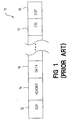
- variable-length frame 11 comprises a 4-byte start-of-frame (SOF) indicator 12, which is a particular binary sequence indicative of the beginning of the frame 11.
- SOF indicator 12 is followed by a 24-byte header 14, which generally specifies, among other things, the frame source address and destination address as well as whether the frame 11 is either control information or actual data.
- the header 14 is followed by a field of variable-length data 16.
- the length of the data 16 is 0 to 2112 bytes.
- the data 16 is followed successively by a 4-byte CRC (cyclical redundancy check) code 17 for error detection, and by a 4 byte end-of-frame (EOF) indicator 18.
- CRC cyclical redundancy check
- EEF end-of-frame
- FIG. 2 illustrates a block diagram of a representative prior art fibre channel architecture in a fibre channel network 100.
- a workstation 120, a mainframe 122 and a super computer 124 are interconnected with various subsystems (e.g., a tape subsystem 126, a disk subsystem 128, and a display subsystem 130) via a fibre channel fabric 110 (i.e. fibre channel switch) .
- the fabric 110 is an entity that interconnects various node-ports (N_ports) and their associated workstations, mainframes and peripherals attached to the fabric 110 through the F_ports.
- the essential function of the fabric 110 is to receive frames of data from a source N_port and, using a first protocol, route the frames to a destination N_port.
- the first protocol is the fibre channel protocol.
- Other protocols, such as the asynchronous transfer mode (ATM) could be used without departing from the scope of the present invention.
- ATM asynchronous transfer mode
- the fibre channel switch 300 illustrated in FIG. 3 employs a plurality of channel modules 340.
- FIG. 3 illustrates two channel modules 340 A and 340 B, the number of channel modules 340 may be greater than illustrated and is typically dependent upon system configuration.
- the fibre channel switch has four (4) channel module cards, each containing four 266 MBaud F_ports (providing for the interconnection of sixteen F_ports and associated computers and peripherals).
- the architecture provides for the substitution of the four 266 Mbaud channel module cards with either dual port 531 Mbaud channel module cards or a single port 1063 MBaud channel module.
- Each channel module 340 is coupled directly to a main link 320, an intermix link 322, a control link 324 and a path status link 326.
- Control signals over the control link 324 direct the transfer of frames received by one channel module 340 to a different port on the same channel module or to any other available channel module 340.
- the channel modules 340 provide port intelligence for data communication with the channels, buffered receive memory for temporarily storing frames for class 2 data transfers, as well as a bypass such that incoming frames are not buffered during class 1 data transfers.
- a path allocation system 350 communicates with the channel modules 340 through a switch module 360.
- the path allocation system 350 collects frame header information for each frame from the receiving ports of channel module 340. The path allocation system 350 verifies the validity of the frame header information and allocates switch resources to set up a path for the frame, through the switch to the destination port. Once the frame has been forwarded, the path allocation system 350 de-allocates the switch resources.
- the path allocation system 350 also collects frame header information for circuit switched traffic (Class 1 connect frames) from the channel modules 340. The path allocation system 350 then verifies the validity of the connection and allocates switch resources to set up a dedicated path for the connection to follow. The connection traffic itself will de-allocate resources.
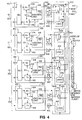
- FIG. 4 shows a block diagram of the channel module architecture for a quad port, 266 Mbaud channel module comprising four port intelligence systems 410 and a memory interface system 420 having four memory interface ASIC's 422, 424, 426 and 428.
- the architecture for a double port, 531 Mbaud channel module implementation would be similar, except that the 531 implementation employs two port intelligence modules 410.
- the architecture for a single port, 1062 Mbaud channel module implementation would be similar, except that the 1062 implementation employs four channel modules 410 coupled to the memory interface systems.
- Each port intelligence system 410 is coupled to external N_ports through a GLM/OLC transceiver 412. Incoming frames are transferred by the GLM/OLC transceiver 412 to a receiver 414. Status/control logic circuit 418 recognizes when a new frame is received by the receiver 414 and determines the transfer class (either 1 or 2) as well as the length of data from the received frame header information attached to the frame.
- the purposes of the receiver 414 are to: maintain synchronization with the attached N_port; decode incoming transmission characters, to manage buffer-to-buffer flow control; gather statistics to evaluate link performance; retime the system clock; detect, check, and validate frames; and forward all frames to the memory interface system 420 for temporary storage in associated receive memory 432, 434, 436 and 438.
- the memory interface system 420 in response to commands from the port intelligence system 410 and the path allocation system 350, employs the four memory interface ASIC's 422, 424, 426 and 428 to interface four receive memories 432, 434, 436 and 438 (16kx16 external RAM) to internal switch data paths via the main bus 320 and imix bus 322.
- Frames transmitted across receive data path 421 between the port intelligence system 410 and the memory interface system 420 are bit sliced such that memory interface 422 receives bits 0-1, memory interface 424 receives bits 2-3, memory interface 426 receives bits 4-5 and memory interface 428 receives bits 6-7.
- Each memory interface knows its position and the baud rate at which the channel module 340 is operating.
- Frames read from receive memories 422, 424, 426 and 428 are reassembled to become byte-wide for traversing the fibre channel switch on the main bus 320 and imix bus 322.
- a transmitter 416 is coupled between the memory interface system 420 and the GLM/OLC transceiver 412 and transmits frames that have been forwarded from other channel module receive memories within the fibre channel switch for encoding and transmission according to fibre channel rules.
- a 4kx9 FIFO transmit memory 442 is coupled between the memory interface 420 and the transmitter 416 for interfacing the main bus 320 and imix bus 322 to the port intelligence system 410.
- the memory interface 420 outputs bit-sliced data that is reformed on the transmit data path 444 at the input of the transmit memory 442.
- Each memory interface 422, 424, 426 and 428 includes a multiplexer 429 for providing class 1 data bypass via connection 431 and buffered storage for class 2 data transfers via connection 433 to the receive memory. Additionally, each memory interface includes a memory control logic 435 for controlling the multiplexers 429, the receive memories 432, 434, 436, 438 and the transmit memory 442 in response to commands from the port intelligence system 410 and the path allocation system 350 (FIG. 3).
- Each receive memory 432, 434, 436 and 438 is comprised of a set of sixteen memory buffers numbered 0-15 (illustrated in the expanded portion 440 of FIG. 4), each having a storage capacity of two kbytes.
- Memory buffers numbered 1 through 14 are designated for frame transfers of class 2, memory buffer numbered 15 is reserved for class 1 frames destined for the embedded N_port on the element controller 358 (Fig. 3), and memory buffer number 0 is reserved for overflow.
- a maximum size frame in accordance with the Fibre Channel industry standard is 2148 bytes long.
- a binary addressing scheme "PPbbbbxxxxxxxxxx" is employed for the fourteen memory buffers numbered 1-14 and PP1111bbbbxxxx for the overflow memory buffer numbered 0, where PP identifies the F_port from which the frame is being transferred and bbbb identifies the memory buffer number at which it currently resides.
- a preferred embodiment of the present invention provides for delaying frames received asynchronously from the fibre channel port until receive memory is properly sequenced for storing the delayed frames.
- a circular buffer is positioned on the data path between the fibre channel port and the receive memory for delaying the frames in accordance with control signals generated by a sequencer having knowledge of the receive memory sequence count.
- frames received asynchronously at port 302 are directed to receiver 414 and bit-sliced into two-bit data for distribution on the data path 421 to the ASIC's 422, 424, 426 and 428.
- Each ASIC includes a sixteen location circular buffer 423 (three-bits wide, two-bits data, one tag bit indicating the start and end of each frame).
- the output of each circular buffer 423 is directed to an accumulator 425 on each ASIC for accumulating eight sets of two-bit wide data into 16-bit wide data for storage in the corresponding receive buffers 432, 434, 436 and 438.
- the logic 435 in each ASIC 422, 424, 426 and 428 further comprises a memory address sequencer 437 that is synchronized to a common system sync pulse.
- Each sequencer 437 is aware of its position (0,1,2,3) in the memory interface 420, the baud rate (266, 531, or 1062) of the port intelligence mechanism 410 and the memory sequencer clock cycle (eight) sequence.
- FIG. 5 provides a more detailed view of the circular buffer 423, accumulator 425, address sequencer 437, and receive buffers 432.
- the preferred embodiment of the invention is implemented in three arrays of sixteen "D-type" flip-flops 423.
- the arrays of flip-flops are coupled to a system clock and the sequencer 437 to provide for a synchronous sequential circuit for delaying asynchronous frames received from the fibre channel.
- FIG. 6 illustrates the operation of the circular buffer in which a write pointer ('wp') 610 controls a write decoder 620 to write data into the 16 flip flops 623 of the circular buffer in accordance with a write enable signal (when 'wr_en' is active).
- the write enable signal is derived from the tag bits associated with valid frame data.
- a read pointer ('rp') is employed for designating the flop-flop to which data should be read out.
- the read pointer 630 advances through the circular buffer whenever the read enable ('rd_en') is active.
- the read enable signal is made active by the memory sequencer which determines when transfers to the accumulator occur. The passing of data to the accumulator is synchronized by providing a read enable to coincide with the time appropriate for sending data to memory.
- the write pointer 620 and the read pointer 630 are pointing at the same flip-flop.
- the write pointer moves down through the 16 flip-flop locations to temporarily store data.
- the read pointer is waiting for a signal from the address sequencer 427 to indicate the time is appropriate to start reading data from the flip flops.
- the first piece of data read out will be the first data written into the flip-flops.
- the read pointer follows the write pointer (with a delay), once the signal from the address sequencer is provided.
Landscapes
- Engineering & Computer Science (AREA)
- Theoretical Computer Science (AREA)
- Physics & Mathematics (AREA)
- General Engineering & Computer Science (AREA)
- General Physics & Mathematics (AREA)
- Signal Processing (AREA)
- Computer Hardware Design (AREA)
- Microelectronics & Electronic Packaging (AREA)
- Computer Networks & Wireless Communication (AREA)
- Power Engineering (AREA)
- Data Exchanges In Wide-Area Networks (AREA)
- Multi Processors (AREA)
- Computer And Data Communications (AREA)
- Synchronisation In Digital Transmission Systems (AREA)
Applications Claiming Priority (2)
| Application Number | Priority Date | Filing Date | Title |
|---|---|---|---|
| US548506 | 1995-10-26 | ||
| US08/548,506 US5872822A (en) | 1995-10-26 | 1995-10-26 | Method and apparatus for memory sequencing |
Publications (1)
| Publication Number | Publication Date |
|---|---|
| EP0772121A1 true EP0772121A1 (de) | 1997-05-07 |
Family
ID=24189138
Family Applications (1)
| Application Number | Title | Priority Date | Filing Date |
|---|---|---|---|
| EP96115847A Ceased EP0772121A1 (de) | 1995-10-26 | 1996-10-02 | Verfahren und Vorrichtung zur Speichersequenzierung |
Country Status (4)
| Country | Link |
|---|---|
| US (1) | US5872822A (de) |
| EP (1) | EP0772121A1 (de) |
| JP (1) | JPH09146906A (de) |
| CA (1) | CA2182422A1 (de) |
Cited By (4)
| Publication number | Priority date | Publication date | Assignee | Title |
|---|---|---|---|---|
| EP1365555A1 (de) * | 2002-05-20 | 2003-11-26 | Texas Instruments Limited | Ringpuffer zur Verzögerungskompensation in paralleler Übertragung |
| WO2003085910A3 (en) * | 2002-04-01 | 2004-02-05 | Andiamo Systems Inc | Methods and apparatus for in-order delivery of fibre channel frames |
| WO2005027448A1 (en) * | 2003-09-11 | 2005-03-24 | Xilinx, Inc. | Channel bonding of a plurality of multi-gigabit transceivers |
| US7616637B1 (en) | 2002-04-01 | 2009-11-10 | Cisco Technology, Inc. | Label switching in fibre channel networks |
Families Citing this family (28)
| Publication number | Priority date | Publication date | Assignee | Title |
|---|---|---|---|---|
| JP3156623B2 (ja) * | 1997-01-31 | 2001-04-16 | 日本電気株式会社 | ファイバチャネルファブリック |
| US6185203B1 (en) | 1997-02-18 | 2001-02-06 | Vixel Corporation | Fibre channel switching fabric |
| US6118776A (en) * | 1997-02-18 | 2000-09-12 | Vixel Corporation | Methods and apparatus for fiber channel interconnection of private loop devices |
| US6317427B1 (en) * | 1997-04-24 | 2001-11-13 | Cabletron Systems, Inc. | Method and apparatus for adaptive port buffering |
| US6038619A (en) * | 1997-05-29 | 2000-03-14 | International Business Machines Corporation | Disk drive initiated data transfers responsive to sequential or near sequential read or write requests |
| JP3228182B2 (ja) | 1997-05-29 | 2001-11-12 | 株式会社日立製作所 | 記憶システム及び記憶システムへのアクセス方法 |
| US6314100B1 (en) | 1998-03-26 | 2001-11-06 | Emulex Corporation | Method of validation and host buffer allocation for unmapped fibre channel frames |
| US6401128B1 (en) * | 1998-08-07 | 2002-06-04 | Brocade Communiations Systems, Inc. | System and method for sending and receiving frames between a public device and a private device |
| US6765919B1 (en) | 1998-10-23 | 2004-07-20 | Brocade Communications Systems, Inc. | Method and system for creating and implementing zones within a fibre channel system |
| US6314477B1 (en) * | 1998-10-30 | 2001-11-06 | Agilent Technologies, Inc. | Performance of fibre channel protocol sequence reassembly using expected frame information and buffer list calculations |
| US6721320B1 (en) * | 1998-12-18 | 2004-04-13 | Lsi Logic Corporation | Method and apparatus for fibre channel identification and retrieval |
| US6667983B1 (en) * | 1999-05-27 | 2003-12-23 | 3Com Corporation | Scaleable priority arbiter for arbitrating between multiple FIFO entry points of a network interface card |
| US20030075253A1 (en) * | 1999-08-26 | 2003-04-24 | Antonio Serra | Process for producing tyres, tyres thus obtained and elastomeric compositions used therein |
| JP2001167040A (ja) | 1999-12-14 | 2001-06-22 | Hitachi Ltd | 記憶サブシステム及び記憶制御装置 |
| JP4651230B2 (ja) | 2001-07-13 | 2011-03-16 | 株式会社日立製作所 | 記憶システム及び論理ユニットへのアクセス制御方法 |
| US6684209B1 (en) * | 2000-01-14 | 2004-01-27 | Hitachi, Ltd. | Security method and system for storage subsystem |
| US7657727B2 (en) * | 2000-01-14 | 2010-02-02 | Hitachi, Ltd. | Security for logical unit in storage subsystem |
| US6636239B1 (en) | 2000-02-24 | 2003-10-21 | Sanavigator, Inc. | Method of operating a graphical user interface to selectively enable and disable a datapath in a network |
| US6571367B1 (en) * | 2000-03-15 | 2003-05-27 | Emc Corporation | Method and apparatus connecting between a fiber channel and a cache memory |
| JP4719957B2 (ja) * | 2000-05-24 | 2011-07-06 | 株式会社日立製作所 | 記憶制御装置及び記憶システム並びに記憶システムのセキュリティ設定方法 |
| US6850498B2 (en) * | 2000-12-22 | 2005-02-01 | Intel Corporation | Method and system for evaluating a wireless link |
| US7366194B2 (en) | 2001-04-18 | 2008-04-29 | Brocade Communications Systems, Inc. | Fibre channel zoning by logical unit number in hardware |
| US6862293B2 (en) * | 2001-11-13 | 2005-03-01 | Mcdata Corporation | Method and apparatus for providing optimized high speed link utilization |
| US7149857B2 (en) | 2002-05-14 | 2006-12-12 | Micron Technology, Inc. | Out of order DRAM sequencer |
| US7219300B2 (en) * | 2002-09-30 | 2007-05-15 | Sanavigator, Inc. | Method and system for generating a network monitoring display with animated utilization information |
| US7352740B2 (en) * | 2003-04-29 | 2008-04-01 | Brocade Communciations Systems, Inc. | Extent-based fibre channel zoning in hardware |
| US7430203B2 (en) * | 2004-01-29 | 2008-09-30 | Brocade Communications Systems, Inc. | Fibre channel zoning hardware for directing a data packet to an external processing device |
| WO2020007447A1 (en) * | 2018-07-03 | 2020-01-09 | Huawei Technologies Co., Ltd. | Device and method for ordering packets |
Citations (2)
| Publication number | Priority date | Publication date | Assignee | Title |
|---|---|---|---|---|
| EP0239937A2 (de) * | 1986-03-31 | 1987-10-07 | Wang Laboratories Inc. | Serielle Übertragungssteuerungsvorrichtung |
| US5299313A (en) * | 1992-07-28 | 1994-03-29 | 3Com Corporation | Network interface with host independent buffer management |
Family Cites Families (8)
| Publication number | Priority date | Publication date | Assignee | Title |
|---|---|---|---|---|
| US4823365A (en) * | 1988-06-28 | 1989-04-18 | Honeywell, Inc. | Synchronization method and elastic buffer circuit |
| US4928275A (en) * | 1989-05-26 | 1990-05-22 | Northern Telecom Limited | Synchronization of asynchronous data signals |
| GB9008374D0 (en) * | 1990-04-12 | 1990-06-13 | British Telecomm | Communication system |
| US5131013A (en) * | 1990-05-30 | 1992-07-14 | At&T Bell Laboratories | Asynchronous-synchronous digital transmission signal conversion |
| JP2600509B2 (ja) * | 1990-09-05 | 1997-04-16 | 富士通株式会社 | ディジタル無線伝送方式 |
| US5426639A (en) * | 1991-11-29 | 1995-06-20 | At&T Corp. | Multiple virtual FIFO arrangement |
| US5457717A (en) * | 1993-11-29 | 1995-10-10 | Dsc Communications Corporation | Apparatus and method for eliminating mapping jitter |
| US5452010A (en) * | 1994-07-18 | 1995-09-19 | Tektronix, Inc. | Synchronizing digital video inputs |
-
1995
- 1995-10-26 US US08/548,506 patent/US5872822A/en not_active Expired - Lifetime
-
1996
- 1996-07-31 CA CA002182422A patent/CA2182422A1/en not_active Abandoned
- 1996-10-02 EP EP96115847A patent/EP0772121A1/de not_active Ceased
- 1996-10-11 JP JP8269477A patent/JPH09146906A/ja active Pending
Patent Citations (2)
| Publication number | Priority date | Publication date | Assignee | Title |
|---|---|---|---|---|
| EP0239937A2 (de) * | 1986-03-31 | 1987-10-07 | Wang Laboratories Inc. | Serielle Übertragungssteuerungsvorrichtung |
| US5299313A (en) * | 1992-07-28 | 1994-03-29 | 3Com Corporation | Network interface with host independent buffer management |
Cited By (8)
| Publication number | Priority date | Publication date | Assignee | Title |
|---|---|---|---|---|
| WO2003085910A3 (en) * | 2002-04-01 | 2004-02-05 | Andiamo Systems Inc | Methods and apparatus for in-order delivery of fibre channel frames |
| US7406034B1 (en) | 2002-04-01 | 2008-07-29 | Cisco Technology, Inc. | Methods and apparatus for fibre channel frame delivery |
| US7616637B1 (en) | 2002-04-01 | 2009-11-10 | Cisco Technology, Inc. | Label switching in fibre channel networks |
| CN1663194B (zh) * | 2002-04-01 | 2010-06-23 | 思科技术公司 | 用于在光纤信道结构中选择性地传递帧的方法和系统 |
| KR100965645B1 (ko) * | 2002-04-01 | 2010-06-23 | 씨스코 테크놀러지, 인코포레이티드 | 파이버 채널 프레임들을 순차적으로 전달하기 위한 방법및 장치 |
| EP1365555A1 (de) * | 2002-05-20 | 2003-11-26 | Texas Instruments Limited | Ringpuffer zur Verzögerungskompensation in paralleler Übertragung |
| WO2005027448A1 (en) * | 2003-09-11 | 2005-03-24 | Xilinx, Inc. | Channel bonding of a plurality of multi-gigabit transceivers |
| US7421014B2 (en) | 2003-09-11 | 2008-09-02 | Xilinx, Inc. | Channel bonding of a plurality of multi-gigabit transceivers |
Also Published As
| Publication number | Publication date |
|---|---|
| JPH09146906A (ja) | 1997-06-06 |
| CA2182422A1 (en) | 1997-04-27 |
| US5872822A (en) | 1999-02-16 |
Similar Documents
| Publication | Publication Date | Title |
|---|---|---|
| US5872822A (en) | Method and apparatus for memory sequencing | |
| US5610745A (en) | Method and apparatus for tracking buffer availability | |
| US6240096B1 (en) | Fibre channel switch employing distributed queuing | |
| US5835496A (en) | Method and apparatus for data alignment | |
| EP1454440B1 (de) | Verfahren und vorrichtung zur bereitstellung einer optimierten ausnutzung schneller strecken | |
| US6031842A (en) | Low latency shared memory switch architecture | |
| US5828475A (en) | Bypass switching and messaging mechanism for providing intermix data transfer for a fiber optic switch using a bypass bus and buffer | |
| US5490007A (en) | Bypass switching and messaging mechanism for providing intermix data transfer for a fiber optic switch | |
| US5502719A (en) | Path allocation system and method having double link list queues implemented with a digital signal processor (DSP) for a high performance fiber optic switch | |
| US5519695A (en) | Switch element for fiber channel networks | |
| US4929939A (en) | High-speed switching system with flexible protocol capability | |
| US6731646B1 (en) | Fibre channel switching system and method | |
| US5603064A (en) | Channel module for a fiber optic switch with bit sliced memory architecture for data frame storage | |
| US5592160A (en) | Method and apparatus for transmission code decoding and encoding | |
| JPH08256168A (ja) | 転送路割り当てシステム | |
| EP0419750B1 (de) | Verteilermechanismus zur Herstellung von Verbindungen zwischen den Benutzer-Schnittstellen eines Kommunikationssystems | |
| EP0505781B1 (de) | Serieller Multimedia Linienschalter für Parallelnetzwerke und ein heterogenes homologes Rechnersystem | |
| EP0170799B1 (de) | Vermittlungssysteme | |
| EP0766429A2 (de) | Verfahren und Vorrichtung zur Pufferverwaltung |
Legal Events
| Date | Code | Title | Description |
|---|---|---|---|
| PUAI | Public reference made under article 153(3) epc to a published international application that has entered the european phase |
Free format text: ORIGINAL CODE: 0009012 |
|
| AK | Designated contracting states |
Kind code of ref document: A1 Designated state(s): DE FR GB |
|
| RAP1 | Party data changed (applicant data changed or rights of an application transferred) |
Owner name: MCDATA CORPORATION |
|
| 17P | Request for examination filed |
Effective date: 19971104 |
|
| 17Q | First examination report despatched |
Effective date: 20010321 |
|
| STAA | Information on the status of an ep patent application or granted ep patent |
Free format text: STATUS: THE APPLICATION HAS BEEN REFUSED |
|
| 18R | Application refused |
Effective date: 20030106 |