EP0772222A1 - Appareil et procédé de traitement par plasma mirco-onde - Google Patents
Appareil et procédé de traitement par plasma mirco-onde Download PDFInfo
- Publication number
- EP0772222A1 EP0772222A1 EP96117351A EP96117351A EP0772222A1 EP 0772222 A1 EP0772222 A1 EP 0772222A1 EP 96117351 A EP96117351 A EP 96117351A EP 96117351 A EP96117351 A EP 96117351A EP 0772222 A1 EP0772222 A1 EP 0772222A1
- Authority
- EP
- European Patent Office
- Prior art keywords
- plasma process
- process chamber
- substrate
- etching
- gas
- Prior art date
- Legal status (The legal status is an assumption and is not a legal conclusion. Google has not performed a legal analysis and makes no representation as to the accuracy of the status listed.)
- Withdrawn
Links
- 238000000034 method Methods 0.000 title claims abstract description 126
- 239000000758 substrate Substances 0.000 claims abstract description 77
- 238000005530 etching Methods 0.000 claims abstract description 63
- 238000004140 cleaning Methods 0.000 claims description 11
- 238000004380 ashing Methods 0.000 claims description 5
- 238000005121 nitriding Methods 0.000 claims description 5
- 238000012545 processing Methods 0.000 claims description 5
- PXBRQCKWGAHEHS-UHFFFAOYSA-N dichlorodifluoromethane Chemical compound FC(F)(Cl)Cl PXBRQCKWGAHEHS-UHFFFAOYSA-N 0.000 claims description 4
- RWRIWBAIICGTTQ-UHFFFAOYSA-N difluoromethane Chemical compound FCF RWRIWBAIICGTTQ-UHFFFAOYSA-N 0.000 claims description 4
- 230000003647 oxidation Effects 0.000 claims description 4
- 238000007254 oxidation reaction Methods 0.000 claims description 4
- FFUAGWLWBBFQJT-UHFFFAOYSA-N hexamethyldisilazane Chemical compound C[Si](C)(C)N[Si](C)(C)C FFUAGWLWBBFQJT-UHFFFAOYSA-N 0.000 claims description 2
- 239000007789 gas Substances 0.000 description 38
- 239000010408 film Substances 0.000 description 21
- VYPSYNLAJGMNEJ-UHFFFAOYSA-N silicon dioxide Inorganic materials O=[Si]=O VYPSYNLAJGMNEJ-UHFFFAOYSA-N 0.000 description 12
- 238000001020 plasma etching Methods 0.000 description 10
- 239000011521 glass Substances 0.000 description 8
- 150000002500 ions Chemical class 0.000 description 8
- 229910021420 polycrystalline silicon Inorganic materials 0.000 description 7
- 229910052710 silicon Inorganic materials 0.000 description 7
- XUIMIQQOPSSXEZ-UHFFFAOYSA-N Silicon Chemical compound [Si] XUIMIQQOPSSXEZ-UHFFFAOYSA-N 0.000 description 6
- 229920005591 polysilicon Polymers 0.000 description 6
- 239000010703 silicon Substances 0.000 description 6
- 229910052681 coesite Inorganic materials 0.000 description 5
- 229910052906 cristobalite Inorganic materials 0.000 description 5
- 238000011156 evaluation Methods 0.000 description 5
- 239000004065 semiconductor Substances 0.000 description 5
- 239000000377 silicon dioxide Substances 0.000 description 5
- 229910052682 stishovite Inorganic materials 0.000 description 5
- 229910052905 tridymite Inorganic materials 0.000 description 5
- 230000005684 electric field Effects 0.000 description 4
- 229910052751 metal Inorganic materials 0.000 description 4
- 239000002184 metal Substances 0.000 description 4
- 229910052782 aluminium Inorganic materials 0.000 description 3
- 238000001816 cooling Methods 0.000 description 3
- 230000000694 effects Effects 0.000 description 3
- 230000004907 flux Effects 0.000 description 3
- 229910010272 inorganic material Inorganic materials 0.000 description 3
- 239000011147 inorganic material Substances 0.000 description 3
- 239000010410 layer Substances 0.000 description 3
- 229910021421 monocrystalline silicon Inorganic materials 0.000 description 3
- 239000011368 organic material Substances 0.000 description 3
- 229910052719 titanium Inorganic materials 0.000 description 3
- 229910017083 AlN Inorganic materials 0.000 description 2
- 229910015844 BCl3 Inorganic materials 0.000 description 2
- WCUXLLCKKVVCTQ-UHFFFAOYSA-M Potassium chloride Chemical compound [Cl-].[K+] WCUXLLCKKVVCTQ-UHFFFAOYSA-M 0.000 description 2
- 229910052581 Si3N4 Inorganic materials 0.000 description 2
- FAPWRFPIFSIZLT-UHFFFAOYSA-M Sodium chloride Chemical compound [Na+].[Cl-] FAPWRFPIFSIZLT-UHFFFAOYSA-M 0.000 description 2
- GWEVSGVZZGPLCZ-UHFFFAOYSA-N Titan oxide Chemical compound O=[Ti]=O GWEVSGVZZGPLCZ-UHFFFAOYSA-N 0.000 description 2
- PNEYBMLMFCGWSK-UHFFFAOYSA-N aluminium oxide Inorganic materials [O-2].[O-2].[O-2].[Al+3].[Al+3] PNEYBMLMFCGWSK-UHFFFAOYSA-N 0.000 description 2
- 229910021417 amorphous silicon Inorganic materials 0.000 description 2
- QVGXLLKOCUKJST-UHFFFAOYSA-N atomic oxygen Chemical compound [O] QVGXLLKOCUKJST-UHFFFAOYSA-N 0.000 description 2
- 229910052593 corundum Inorganic materials 0.000 description 2
- 239000005357 flat glass Substances 0.000 description 2
- PQXKHYXIUOZZFA-UHFFFAOYSA-M lithium fluoride Chemical compound [Li+].[F-] PQXKHYXIUOZZFA-UHFFFAOYSA-M 0.000 description 2
- 229910052750 molybdenum Inorganic materials 0.000 description 2
- 239000001301 oxygen Substances 0.000 description 2
- 229910052760 oxygen Inorganic materials 0.000 description 2
- -1 polyethylene Polymers 0.000 description 2
- 239000010453 quartz Substances 0.000 description 2
- 238000000926 separation method Methods 0.000 description 2
- 239000002344 surface layer Substances 0.000 description 2
- 229910052715 tantalum Inorganic materials 0.000 description 2
- 239000010409 thin film Substances 0.000 description 2
- FAQYAMRNWDIXMY-UHFFFAOYSA-N trichloroborane Chemical compound ClB(Cl)Cl FAQYAMRNWDIXMY-UHFFFAOYSA-N 0.000 description 2
- 229910001845 yogo sapphire Inorganic materials 0.000 description 2
- 229910001369 Brass Inorganic materials 0.000 description 1
- 229910001218 Gallium arsenide Inorganic materials 0.000 description 1
- 239000004962 Polyamide-imide Substances 0.000 description 1
- 239000004698 Polyethylene Substances 0.000 description 1
- 239000004642 Polyimide Substances 0.000 description 1
- 239000004743 Polypropylene Substances 0.000 description 1
- 239000004793 Polystyrene Substances 0.000 description 1
- 229920001328 Polyvinylidene chloride Polymers 0.000 description 1
- ATJFFYVFTNAWJD-UHFFFAOYSA-N Tin Chemical compound [Sn] ATJFFYVFTNAWJD-UHFFFAOYSA-N 0.000 description 1
- 230000002159 abnormal effect Effects 0.000 description 1
- 229910045601 alloy Inorganic materials 0.000 description 1
- 239000000956 alloy Substances 0.000 description 1
- 229910052785 arsenic Inorganic materials 0.000 description 1
- 229910001632 barium fluoride Inorganic materials 0.000 description 1
- 239000010951 brass Substances 0.000 description 1
- WUKWITHWXAAZEY-UHFFFAOYSA-L calcium difluoride Chemical compound [F-].[F-].[Ca+2] WUKWITHWXAAZEY-UHFFFAOYSA-L 0.000 description 1
- 229910001634 calcium fluoride Inorganic materials 0.000 description 1
- 229920002301 cellulose acetate Polymers 0.000 description 1
- 229910052804 chromium Inorganic materials 0.000 description 1
- 230000006378 damage Effects 0.000 description 1
- 230000010354 integration Effects 0.000 description 1
- 229910052742 iron Inorganic materials 0.000 description 1
- 229910052745 lead Inorganic materials 0.000 description 1
- 239000004973 liquid crystal related substance Substances 0.000 description 1
- 229910001635 magnesium fluoride Inorganic materials 0.000 description 1
- CPLXHLVBOLITMK-UHFFFAOYSA-N magnesium oxide Inorganic materials [Mg]=O CPLXHLVBOLITMK-UHFFFAOYSA-N 0.000 description 1
- 238000004519 manufacturing process Methods 0.000 description 1
- 150000002739 metals Chemical class 0.000 description 1
- 238000012986 modification Methods 0.000 description 1
- 230000004048 modification Effects 0.000 description 1
- 229910003465 moissanite Inorganic materials 0.000 description 1
- 230000007935 neutral effect Effects 0.000 description 1
- 229910052759 nickel Inorganic materials 0.000 description 1
- 150000004767 nitrides Chemical class 0.000 description 1
- 230000003287 optical effect Effects 0.000 description 1
- 230000001590 oxidative effect Effects 0.000 description 1
- 239000005360 phosphosilicate glass Substances 0.000 description 1
- 229910052697 platinum Inorganic materials 0.000 description 1
- 229920002312 polyamide-imide Polymers 0.000 description 1
- 229920000515 polycarbonate Polymers 0.000 description 1
- 239000004417 polycarbonate Substances 0.000 description 1
- 229920000728 polyester Polymers 0.000 description 1
- 229920000573 polyethylene Polymers 0.000 description 1
- 229920001721 polyimide Polymers 0.000 description 1
- 229920001155 polypropylene Polymers 0.000 description 1
- 229920002223 polystyrene Polymers 0.000 description 1
- 229920000915 polyvinyl chloride Polymers 0.000 description 1
- 239000004800 polyvinyl chloride Substances 0.000 description 1
- 239000005033 polyvinylidene chloride Substances 0.000 description 1
- 230000007261 regionalization Effects 0.000 description 1
- 238000011160 research Methods 0.000 description 1
- 229910010271 silicon carbide Inorganic materials 0.000 description 1
- 239000011780 sodium chloride Substances 0.000 description 1
- 239000010935 stainless steel Substances 0.000 description 1
- 229910001220 stainless steel Inorganic materials 0.000 description 1
- PBCFLUZVCVVTBY-UHFFFAOYSA-N tantalum pentoxide Inorganic materials O=[Ta](=O)O[Ta](=O)=O PBCFLUZVCVVTBY-UHFFFAOYSA-N 0.000 description 1
- 229910052718 tin Inorganic materials 0.000 description 1
- 229910052721 tungsten Inorganic materials 0.000 description 1
- 229910052720 vanadium Inorganic materials 0.000 description 1
- XLYOFNOQVPJJNP-UHFFFAOYSA-N water Substances O XLYOFNOQVPJJNP-UHFFFAOYSA-N 0.000 description 1
- 229910052725 zinc Inorganic materials 0.000 description 1
Images

Classifications
-
- H—ELECTRICITY
- H01—ELECTRIC ELEMENTS
- H01J—ELECTRIC DISCHARGE TUBES OR DISCHARGE LAMPS
- H01J37/00—Discharge tubes with provision for introducing objects or material to be exposed to the discharge, e.g. for the purpose of examination or processing thereof
- H01J37/32—Gas-filled discharge tubes
- H01J37/32009—Arrangements for generation of plasma specially adapted for examination or treatment of objects, e.g. plasma sources
- H01J37/32192—Microwave generated discharge
- H01J37/32211—Means for coupling power to the plasma
- H01J37/32229—Waveguides
-
- H—ELECTRICITY
- H01—ELECTRIC ELEMENTS
- H01J—ELECTRIC DISCHARGE TUBES OR DISCHARGE LAMPS
- H01J37/00—Discharge tubes with provision for introducing objects or material to be exposed to the discharge, e.g. for the purpose of examination or processing thereof
- H01J37/32—Gas-filled discharge tubes
- H01J37/32009—Arrangements for generation of plasma specially adapted for examination or treatment of objects, e.g. plasma sources
- H01J37/32192—Microwave generated discharge
-
- H—ELECTRICITY
- H01—ELECTRIC ELEMENTS
- H01J—ELECTRIC DISCHARGE TUBES OR DISCHARGE LAMPS
- H01J37/00—Discharge tubes with provision for introducing objects or material to be exposed to the discharge, e.g. for the purpose of examination or processing thereof
- H01J37/32—Gas-filled discharge tubes
- H01J37/32431—Constructional details of the reactor
- H01J37/32697—Electrostatic control
- H01J37/32706—Polarising the substrate
Definitions
- the present invention relates to a microwave plasma process apparatus.
- the apparatus enables etching of large-area substrates in super fine patterns at high speed. Further, the apparatus can be applied to oxidation, nitriding, doping, cleaning, cleaning ashing, and so on.
- the reactive ion etching (RIE) apparatus for applying RF (radio frequency) power between parallel plate electrodes opposed to each other is frequently used for pattern formation in fabrication of electronic components such as ultra-large-scale integrated (ULSI) circuits.
- RIE reactive ion etching
- a conventional RIE apparatus is shown in Fig. 2.
- a process chamber 201 there are provided a holder 203 for a substrate 202 to be processed, and a gas introducing means 204.
- An RF power supply 206 is connected to the holder 203.
- the process chamber is evacuated by an evacuation means 205.
- Etching is carried out as follows.
- the inside of the process chamber 201 is evacuated to a vacuum through the evacuation means 205.
- etching gas is introduced at a predetermined flow rate through the gas introducing means 204 into the process chamber.
- a conductance valve (not shown) set in the evacuation means 205 is adjusted to keep the inside of the process chamber 201 at a predetermined pressure.
- Desired power is supplied from the RF power supply 206 to the substrate holder 203. Electrons are accelerated by an RF electric field to generate a plasma in the process chamber 201.
- the plasma ionizes the etching gas, and ions produced thereby are accelerated by a self-bias electric field formed near the substrate 202 to impinge upon the surface of the substrate, thereby etching the surface.
- the conventional RIE apparatus It is, however, not easy for the conventional RIE apparatus to achieve discharge under low pressures of about 10 -3 Torr, under which anisotropy of ion incidence directions can be maintained, and therefore, the conventional RIE apparatus is not effective in performing anisotropic etching of fine patterns. With increase of integration of devices demand is increasing for further making the patterns finer, but the conventional apparatus fails to meet this demand.
- ECR electron cyclotron resonance
- An ECR etching apparatus is shown in Fig. 3.
- a process chamber 301 there are provided a holder 303 for a substrate 302 to be processed, and a gas introducing means 304.
- An RF power supply 306 is connected to the holder 303.
- the process chamber is evacuated by an evacuation means 305. Further, in the process chamber the microwave is introduced through a microwave introducing window 307 and a magnetic field can be generated by a magnetic field generating means 308.
- Etching is carried out as follows.
- the inside of the process chamber 301 is evacuated to a vacuum through the evacuation means 305.
- the etching gas is introduced at a predetermined flow rate through the gas introducing means 304 into the process chamber 301.
- a conductance valve (not shown) set in the evacuation means 305 is adjusted to keep the inside of the process chamber 301 at a predetermined pressure.
- the magnetic field of 875 G is generated in the process chamber 301 by the magnetic field generating means 308 and microwave power is introduced through the microwave introducing window 307 into the process chamber 301 to generate a plasma.
- Electrons helically move around magnetic lines of force, and when the frequency of rotation of the electrons comes to coincide with the frequency (normally 2.45 GHz) of the microwave (in the case of the magnetic flux density 875 G), the electrons resonantly absorb the microwave to be accelerated. Further, the electrons ionize neutral molecules by bombardment, thereby forming a high-density plasma.
- desired power is supplied from the RF power supply 306 to the support holder 303 at this time, the ions are accelerated by the self-bias electric field formed near the substrate 302 to impinge upon the surface of the substrate, thereby etching the surface.
- ECR etching apparatus permits discharge to occur even under the low-pressure condition of about 1 mTorr, which enables anisotropic etching of fine patterns.
- the ECR etching apparatus as shown in Fig. 3, however, is not easy to generate a uniform magnetic field, so that the apparatus has a problem of nonuniformity of etching and a problem of device destruction due to charge separation in a direction along the surface of the substrate. Because of high temperatures of electrons, in the case of processing of fine patterns with high aspect ratios, abnormal etching (notch) is also likely to be caused by charge separation in a direction along the depth of the substrate.
- An object of the present invention is to provide a plasma process apparatus and method, solving the problems in the conventional plasma process apparatus as described above, that can generate a uniform plasma in high density and in a large area even under the low-pressure condition of about 1 mTorr without using the magnetic field, thereby enabling etching of large-area substrates in super fine patterns and at high speed.
- a plasma process apparatus comprises a plasma process chamber, substrate-to-be-processed supporting means disposed in the process chamber, gas introducing means, evacuation means, microwave introducing means using an endless circular waveguide having a plurality of slots arranged around the process chamber, and RF power supplying means for supplying RF power to the substrate supporting means.
- This arrangement permits the uniform plasma to be generated in high density and in a large area even under the low-pressure condition of about 1 mTorr without using the magnetic field, thereby enabling etching of large-area substrates in super fine patterns and at high speed.
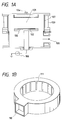
- a microwave plasma process apparatus of the present invention is shown in Fig. 1A.
- a process chamber 101 there are provided a holder 103 for a substrate 102 to be processed, and a processing-gas introducing means 104.
- An RF power supply 106 is connected to the holder 103.
- the process chamber is evacuated by an evacuation means 105.
- an endless circular multi-slot waveguide 109 is provided with intervention of a quartz tube 107.
- the endless circular multi-slot waveguide 109 is shown in Fig. 1B.
- the microwave is guided through a microwave introducing portion 110 and is emitted through a plurality of slots 111 provided in the annular internal wall.
- the process is carried out as follows.
- the inside of the process chamber 101 is evacuated to a vacuum through the evacuation means 105.
- the etching gas is introduced at a predetermined flow rate through the gas inlet port 104 into the process chamber 101.
- a conductance valve (not shown) set in the evacuation means 105 is adjusted to keep the inside of the process chamber 101 at a predetermined pressure. Desired power is supplied from a microwave power supply (not shown) through the waveguide 109 into the process chamber 101, thereby generating a plasma.
- the uniform plasma can be generated in high density and in a large area even under the low-pressure condition of about 1 mTorr without using the magnetic field, thereby enabling etching of the large-area substrate in ultra fine patterns and at high speed.
- the microwave frequency used in the microwave plasma process apparatus of the present invention may be properly selected from the range of 0.8 GHz to 20 GHz.
- the shape of the waveguide used in the plasma process apparatus of the present invention may be not only cylindrical, but also of any other shape, for example, of a disk or polygon, depending upon the configuration of the process chamber.
- the plasma process apparatus of the present invention may further use a magnetic field generating means in addition to the above arrangement. Desired conditions of the magnetic field are those of the cusped magnetic field which has node planes lying on planes including the centers of the plural slots in the endless circular multi-slot waveguide and has magnetic lines of force substantially normal to the substrate supporting means and in which the magnetic flux density of the magnetic field near the slots is greater than that near the substrate.
- the magnetic field generating means may be either a coil or a permanent magnet.
- a water cooling mechanism or any other cooling means such as air cooling means may be used in order to prevent overheat.
- the pressure in the process chamber in the plasma process method of the present invention may be selected preferably from the range of 0.2 mTorr to 10.0 mTorr.
- Thin films that can be processed by the plasma etching method of the present invention include electrically insulating films of Si 3 N 4 , SiO 2 , Ta 2 O 5 , TiO 2 , TiN, Al 2 O 3 , AlN, MgF 2 , and so on; semiconductor films of a-Si (amorphous Si), poly-Si, SiC, GaAs, and so on; metal films of Al, W, Mo, Ti, Ta, and so on, etc., and the various thin films can be etched with efficiency.
- the substrate to be processed by the plasma etching method of the present invention may be either one of semiconductor substrates, electrically conductive substrates, and electrically insulating substrates.
- electrically conductive substrates include metals such as Fe, Ni, Cr, Al, Mo, Au, Nb, Ta, V, Ti, Pt, and Pb; and alloys thereof, for example brass and stainless steel.
- the electrically insulating substrates include various glasses such as SiO 2 -based quartz; inorganic materials such as Si 3 N 4 , NaCl, KCl, LiF, CaF 2 , BaF 2 , Al 2 O 3 , AlN, and MgO; films and sheets of organic materials such as polyethylene, polyester, polycarbonate, cellulose acetate, polypropylene, polyvinyl chloride, polyvinylidene chloride, polystyrene, polyamide, and polyimide.
- glasses such as SiO 2 -based quartz
- inorganic materials such as Si 3 N 4 , NaCl, KCl, LiF, CaF 2 , BaF 2 , Al 2 O 3 , AlN, and MgO
- films and sheets of organic materials such as polyethylene, polyester, polycarbonate, cellulose acetate, polypropylene, polyvinyl chloride, polyvinylidene chloride, polystyrene, polyamide, and polyimide.
- the etching gas used in the plasma etching method of the present invention may be selected from generally well-known gases. Specifically, depending upon the film or substrate to be etched, the etching gas may be selected from F 2 , CF 4 , CH 2 F 2 , C 2 F 6 , CF 2 Cl 2 , SF 6 , and NF 3 .
- the plasma process apparatus and method of the present invention can also be applied to modification of surface, cleaning, resist ashing, or the like, as well as etching.
- etching For example, using Si, Al, Ti, Zn, or Ta as a substrate or surface layer, the substrate or surface layer of these can be subject to oxidation or nitriding or to doping with B, As, or P.
- Another application is a cleaning ashing process for removing organic materials including the resist, inorganic materials, and metal from the surface of the substrate.
- oxidizing gas may be selected from O 2 , O 3 , H 2 O, NO, N 2 O, and NO 2 .
- nitriding gas may be selected from N 2 , NH 3 , N 2 H 4 , and hexamethyldisilazane (HMDS).
- cleaning gas may be selected from O 2 , O 3 , H 2 O, NO, N 2 O, and NO 2 .
- cleaning gas may be selected from F 2 , CF 4 , CH 2 F 2 , C 2 F 6 , CF 2 Cl 2 , SF 6 , and NF 3 .
- etching was carried out on a polysilicon film between the gate electrodes of semiconductor device.
- the substrate 102 used herein was a p-type single-crystal silicon substrate (face orientation ⁇ 100 ⁇ and resistivity 10 ⁇ cm) with a polysilicon film formed as an uppermost layer.
- the inside of the process chamber 101 was evacuated to a vacuum through the evacuation system 105, so as to decrease the pressure down to the value of 10 -6 Torr.
- the gas inlet port 104 CF 4 gas and oxygen were introduced at 300 sccm and at 20 sccm, respectively, into the process chamber 101.
- the conductance valve (not shown) set in the evacuation system 105 was adjusted to keep the inside of the process chamber 101 at 1.0 mTorr.
- the RF wave of 13.56 MHz was applied from the RF power supply 106 to the substrate holder 103, and the power of 1.5 kW was supplied from the microwave power supply of 2.45 GHz through the circular waveguide 109 into the process chamber 101.
- the plasma was generated in the process chamber 101.
- the CF 4 gas and oxygen introduced through the gas inlet port 104 were excited and decomposed in the process chamber 101 to become active species.
- the active species were transported toward the silicon substrate 102 and the ions accelerated by the self-bias etched the polysilicon film.
- etching rate was carried out as to the etching rate, etch selectivity, and etching shape.
- the etching shape was evaluated by observing cross sections of the etched polysilicon film by a scanning electron microscope (SEM). The results confirmed that the etching rate and etch selectivity over SiO 2 were good as 600 nm/min and 30, respectively, and that the microloading effect was little.
- etching was conducted on a BPSG (Boron-doped Phospho-Silicate Glass) film of semiconductor device.
- the substrate 102 used herein was a p-type single-crystal silicon substrate (face orientation ⁇ 100 ⁇ and resistivity 10 ⁇ cm) with a BPSG film 1 ⁇ m thick formed on polysilicon pattern (lines and spaces of 0.5 ⁇ m).
- the inside of the process chamber 101 was evacuated to a vacuum through the evacuation system 105, so as to decrease the pressure down to the value of 10 -6 Torr.
- CF 4 was introduced at the flow rate of 300 sccm through the gas inlet port 104 into the process chamber 101.
- the conductance valve (not shown) set in the evacuation system 105 was adjusted to keep the inside of the process chamber 101 at 1.2 mTorr.
- the power of 2.0 kW was supplied from the microwave power supply of 2.45 GHz through the circular waveguide 109 into the process chamber 101.
- the plasma was generated in the process chamber 101.
- the CF 4 gas introduced through the gas inlet port 104 was excited and decomposed in the process chamber 101 to become an active species.
- the active species was transported toward the silicon substrate 102 to etch the BPSG film.
- etching rate was evaluated by observing cross sections of the etched BPSG film by the scanning electron microscope (SEM). The results confirmed that the etching rate and etch selectivity over polysilicon were good as 300 nm/min and 30, respectively, that the etching shape was almost vertical, and that the microloading effect was little.
- etching was effected on an Al film of multilayer wiring of semiconductor device.
- the substrate 102 used herein was a p-type single-crystal silicon substrate (face orientation ⁇ 100 ⁇ and resistivity 10 ⁇ cm) with an Al film formed as an uppermost layer.
- the inside of the process chamber 101 was evacuated to a vacuum through the evacuation system 105, so as to decrease the pressure down to the value of 10 -6 Torr.
- Cl 2 gas and gasified BCl 3 were introduced at 120 sccm and at 80 sccm, respectively, through the gas inlet port 104 into the process chamber 101.
- the conductance valve (not shown) set in the evacuation system 105 was adjusted to keep the inside of the process chamber 101 at 0.8 mTorr.
- the RF wave of 13.56 MHz was applied from the RF applying means 106 to the substrate holder 103 and the power of 1.2 kW was supplied from the microwave power supply of 2.45 GHz through the circular waveguide 109 into the process chamber 101.
- the plasma was generated in the process chamber 101.
- the Cl 2 gas and BCl 3 introduced through the gas inlet port 104 were excited and decomposed in the process chamber 101 to become active species.
- the active species were transported toward the silicon substrate 102, so that the ions accelerated by the self-bias etched the Al film.
- etching rate was carried out as to the etching rate, etch selectivity, and etching shape.
- the etching shape was evaluated by observing cross sections of the etched Al film by the scanning electron microscope (SEM). The results confirmed that the etching rate and etch selectivity over SiO 2 were good as 500 nm/min and 20, respectively, that the etching shape was vertical, and that the microloading effect was little.
- etching was effected on an Al film of wiring of liquid crystal display element.
- the substrate 102 used herein was a blue plate glass substrate of 450 mm ⁇ 550 mm with an Al film formed as an uppermost layer.
- the inside of the process chamber 101 was evacuated to a vacuum through the evacuation system 105, so as to decrease the pressure down to the value of 10 -6 Torr.
- Cl 2 gas was introduced at the flow rate of 200 sccm through the gas inlet port 104 into the process chamber 101.
- the conductance valve (not shown) set in the evacuation system 105 was adjusted to keep the inside of the process chamber 101 at 2.0 mTorr.
- the RF wave of 13.56 MHz was applied from the RF applying means 106 to the substrate holder 103 and the power of 2.0 kW was supplied from the microwave power supply of 2.45 GHz through the circular waveguide 109 into the process chamber 101.
- the Cl 2 gas introduced through the gas inlet port 104 was excited and decomposed in the process chamber 101 to become an active species.
- the active species was transported toward the glass substrate 102, so that the ions accelerated by the self-bias etched the Al film.
- etching rate was carried out as to the etching rate, etch selectivity, and etching shape.
- the etching shape was evaluated by observing cross sections of the etched Al film by the scanning electron microscope (SEM). The results confirmed that the etching rate and etch selectivity over SiO 2 were good as 500 nm/min and 25, respectively, and that the etching shape was vertical.
- etching was carried out on a glass substrate for phase grating filter of copier optical system.
- the substrate 102 used herein was a white plate glass substrate.
- the inside of the process chamber 101 was evacuated to a vacuum through the evacuation system 105, so as to decrease the pressure down to the value of 10 -6 Torr.
- CF 4 and H 2 were introduced at 200 sccm and at 40 sccm, respectively, through the gas inlet port 104 into the process chamber 101.
- the conductance valve (not shown) set in the evacuation system 105 was adjusted to keep the inside of the process chamber 101 at 1.2 mTorr.
- the RF wave of 13.56 MHz was applied from the RF applying means 106 to the substrate holder 103 and the power of 2.2 kW was supplied from the microwave power supply of 2.45 GHz through the circular waveguide 109 into the process chamber 101.
- the plasma was generated in the process chamber 101.
- the CF 4 gas and H 2 introduced through the gas inlet port 104 were excited and decomposed in the process chamber 101 to become active species.
- the active species were transported toward the glass substrate 102, so that the ions accelerated by the self-bias etched the glass substrate.
- etching rate was good as 450 nm/min and that the etching shape was vertical.
- a plasma process apparatus comprises a plasma process chamber, substrate-to-be-processed supporting means for supporting a substrate to be processed, provided in the process chamber, gas introducing means, gas evacuation means, microwave introducing means using an endless circular waveguide having a plurality of slots arranged around the process chamber, and radio frequency power supplying means for supplying radio frequency power to the substrate supporting means.
- the above arrangement permits a uniform plasma to be generated in high density and in a large area even under the low-pressure condition of about 1 mTorr without using a magnetic field, thus enabling etching of large-area substrates in super fine patterns and at high speed.
Landscapes
- Physics & Mathematics (AREA)
- Engineering & Computer Science (AREA)
- Plasma & Fusion (AREA)
- Chemical & Material Sciences (AREA)
- Analytical Chemistry (AREA)
- Drying Of Semiconductors (AREA)
- ing And Chemical Polishing (AREA)
Applications Claiming Priority (2)
| Application Number | Priority Date | Filing Date | Title |
|---|---|---|---|
| JP285083/95 | 1995-11-01 | ||
| JP7285083A JPH09129607A (ja) | 1995-11-01 | 1995-11-01 | マイクロ波プラズマエッチング装置及び方法 |
Publications (1)
| Publication Number | Publication Date |
|---|---|
| EP0772222A1 true EP0772222A1 (fr) | 1997-05-07 |
Family
ID=17686925
Family Applications (1)
| Application Number | Title | Priority Date | Filing Date |
|---|---|---|---|
| EP96117351A Withdrawn EP0772222A1 (fr) | 1995-11-01 | 1996-10-29 | Appareil et procédé de traitement par plasma mirco-onde |
Country Status (4)
| Country | Link |
|---|---|
| US (1) | US5983829A (fr) |
| EP (1) | EP0772222A1 (fr) |
| JP (1) | JPH09129607A (fr) |
| KR (1) | KR100270269B1 (fr) |
Cited By (2)
| Publication number | Priority date | Publication date | Assignee | Title |
|---|---|---|---|---|
| WO1999038189A1 (fr) * | 1998-01-27 | 1999-07-29 | Fraunhofer-Gesellschaft zur Förderung der angewandten Forschung e.V. | Reacteur a plasma |
| WO2024226583A1 (fr) * | 2023-04-25 | 2024-10-31 | Applied Materials, Inc. | Procédé de nettoyage au plasma de tubes de silice fusionnés |
Families Citing this family (14)
| Publication number | Priority date | Publication date | Assignee | Title |
|---|---|---|---|---|
| US6286939B1 (en) * | 1997-09-26 | 2001-09-11 | Hewlett-Packard Company | Method of treating a metal surface to increase polymer adhesion |
| JPH11193468A (ja) * | 1997-12-30 | 1999-07-21 | Shimadzu Corp | 薄膜形成装置 |
| TW409487B (en) * | 1998-04-10 | 2000-10-21 | Sumitomo Metal Ind | Microwave plasma treatment apparatus and microwave plasma treatment method |
| US6182851B1 (en) * | 1998-09-10 | 2001-02-06 | Applied Materials Inc. | Vacuum processing chambers and method for producing |
| JP3352418B2 (ja) | 1999-01-28 | 2002-12-03 | キヤノン株式会社 | 減圧処理方法及び減圧処理装置 |
| JP4441038B2 (ja) * | 2000-02-07 | 2010-03-31 | 東京エレクトロン株式会社 | マイクロ波プラズマ処理装置 |
| US6441838B1 (en) | 2001-01-19 | 2002-08-27 | Hewlett-Packard Company | Method of treating a metal surface to increase polymer adhesion |
| JP4540926B2 (ja) * | 2002-07-05 | 2010-09-08 | 忠弘 大見 | プラズマ処理装置 |
| JP2008181710A (ja) * | 2007-01-23 | 2008-08-07 | Canon Inc | プラズマ処理装置及び方法 |
| EP2101547B1 (fr) * | 2008-03-11 | 2014-03-05 | Vita Zahnfabrik H. Rauter GmbH & Co. KG | Four de frittage dentaire et procédé de frittage d'éléments dentaires céramiques |
| US8802545B2 (en) * | 2011-03-14 | 2014-08-12 | Plasma-Therm Llc | Method and apparatus for plasma dicing a semi-conductor wafer |
| WO2014159449A1 (fr) * | 2013-03-14 | 2014-10-02 | Tokyo Electron Limited | Dispositif de traitement au plasma d'onde de surface ou micro-ondes |
| US9881804B2 (en) | 2015-01-26 | 2018-01-30 | Tokyo Electron Limited | Method and system for high precision etching of substrates |
| KR20170122185A (ko) * | 2015-11-09 | 2017-11-03 | 후루카와 덴키 고교 가부시키가이샤 | 반도체 칩의 제조방법 및 이것에 이용하는 마스크 일체형 표면 보호 테이프 |
Citations (4)
| Publication number | Priority date | Publication date | Assignee | Title |
|---|---|---|---|---|
| EP0047663A2 (fr) * | 1980-09-10 | 1982-03-17 | Hitachi, Ltd. | Gravure par plasma à micro-ondes |
| JPH05345982A (ja) * | 1991-11-05 | 1993-12-27 | Canon Inc | 無端環状導波管を有するマイクロ波導入装置及び 該装置を備えたプラズマ処理装置 |
| EP0593931A1 (fr) * | 1992-10-23 | 1994-04-27 | Engemann, Jürgen Prof. Dr.-Ing. | Dispositif de production de plasmas micro-ondes |
| US5366586A (en) * | 1992-02-03 | 1994-11-22 | Nec Corporation | Plasma formation using electron cyclotron resonance and method for processing substrate by using the same |
Family Cites Families (6)
| Publication number | Priority date | Publication date | Assignee | Title |
|---|---|---|---|---|
| DE3750115T2 (de) * | 1986-10-20 | 1995-01-19 | Hitachi Ltd | Plasmabearbeitungsgerät. |
| US5134965A (en) * | 1989-06-16 | 1992-08-04 | Hitachi, Ltd. | Processing apparatus and method for plasma processing |
| US5037666A (en) * | 1989-08-03 | 1991-08-06 | Uha Mikakuto Precision Engineering Research Institute Co., Ltd. | High-speed film forming method by microwave plasma chemical vapor deposition (CVD) under high pressure |
| WO2004089046A1 (fr) * | 1991-11-05 | 2004-10-14 | Nobumasa Suzuki | Appareil d'introduction d'ondes ultracourtes comportant un guide d'onde en forme d'anneau sans fin et installation de traitement au plasma comprenant cet appareil |
| JP2989063B2 (ja) * | 1991-12-12 | 1999-12-13 | キヤノン株式会社 | 薄膜形成装置および薄膜形成方法 |
| JPH06216072A (ja) * | 1993-01-13 | 1994-08-05 | Kobe Steel Ltd | プラズマ処理装置へのマイクロ波供給方法 |
-
1995
- 1995-11-01 JP JP7285083A patent/JPH09129607A/ja active Pending
-
1996
- 1996-10-29 EP EP96117351A patent/EP0772222A1/fr not_active Withdrawn
- 1996-10-29 US US08/739,212 patent/US5983829A/en not_active Expired - Lifetime
- 1996-10-31 KR KR1019960050587A patent/KR100270269B1/ko not_active Expired - Fee Related
Patent Citations (4)
| Publication number | Priority date | Publication date | Assignee | Title |
|---|---|---|---|---|
| EP0047663A2 (fr) * | 1980-09-10 | 1982-03-17 | Hitachi, Ltd. | Gravure par plasma à micro-ondes |
| JPH05345982A (ja) * | 1991-11-05 | 1993-12-27 | Canon Inc | 無端環状導波管を有するマイクロ波導入装置及び 該装置を備えたプラズマ処理装置 |
| US5366586A (en) * | 1992-02-03 | 1994-11-22 | Nec Corporation | Plasma formation using electron cyclotron resonance and method for processing substrate by using the same |
| EP0593931A1 (fr) * | 1992-10-23 | 1994-04-27 | Engemann, Jürgen Prof. Dr.-Ing. | Dispositif de production de plasmas micro-ondes |
Non-Patent Citations (1)
| Title |
|---|
| PATENT ABSTRACTS OF JAPAN vol. 018, no. 191 (C - 1186) 4 April 1994 (1994-04-04) * |
Cited By (3)
| Publication number | Priority date | Publication date | Assignee | Title |
|---|---|---|---|---|
| WO1999038189A1 (fr) * | 1998-01-27 | 1999-07-29 | Fraunhofer-Gesellschaft zur Förderung der angewandten Forschung e.V. | Reacteur a plasma |
| US6645343B1 (en) | 1998-01-27 | 2003-11-11 | Fraunhofer-Gesellschaft zur Förderung der angewandten Forschung e.V. | Plasma reactor |
| WO2024226583A1 (fr) * | 2023-04-25 | 2024-10-31 | Applied Materials, Inc. | Procédé de nettoyage au plasma de tubes de silice fusionnés |
Also Published As
| Publication number | Publication date |
|---|---|
| JPH09129607A (ja) | 1997-05-16 |
| US5983829A (en) | 1999-11-16 |
| KR100270269B1 (ko) | 2000-10-16 |
Similar Documents
| Publication | Publication Date | Title |
|---|---|---|
| US5662819A (en) | Plasma processing method with controlled ion/radical ratio | |
| US5983829A (en) | Microwave plasma etching apparatus | |
| KR100274306B1 (ko) | 에칭방법 | |
| JP5581366B2 (ja) | プラズマ処理装置 | |
| KR101880831B1 (ko) | 가스 펄싱을 사용하는 딥 실리콘 에칭 방법 | |
| US6489248B2 (en) | Method and apparatus for etch passivating and etching a substrate | |
| US5354417A (en) | Etching MoSi2 using SF6, HBr and O2 | |
| US5449433A (en) | Use of a high density plasma source having an electrostatic shield for anisotropic polysilicon etching over topography | |
| US5980768A (en) | Methods and apparatus for removing photoresist mask defects in a plasma reactor | |
| KR100413894B1 (ko) | 플라즈마에칭방법 | |
| EP0954877B1 (fr) | Procede pour reduire les dommages dus aux charges induites par un plasma | |
| WO1997036322A1 (fr) | Techniques et appareil permettant de minimiser la charge de la vitesse de gravure | |
| US5880033A (en) | Method for etching metal silicide with high selectivity to polysilicon | |
| US6156663A (en) | Method and apparatus for plasma processing | |
| WO1998028785A1 (fr) | Procede pour ameliorer la selectivite par photoresist et reduire les effets de charge de la vitesse de gravure | |
| US5972235A (en) | Plasma etching using polycarbonate mask and low pressure-high density plasma | |
| US5849641A (en) | Methods and apparatus for etching a conductive layer to improve yield | |
| US6017825A (en) | Etch rate loading improvement | |
| US20040256353A1 (en) | Method and system for deep trench silicon etch | |
| US5728261A (en) | Magnetically enhanced radio frequency reactive ion etching method and apparatus | |
| US4554047A (en) | Downstream apparatus and technique | |
| JP2837556B2 (ja) | プラズマ反応装置とそれを用いた基板の処理方法 | |
| JP3445584B2 (ja) | 反射防止膜のエッチング方法 | |
| JP2515833B2 (ja) | マイクロ波プラズマ処理方法 | |
| JP3516741B2 (ja) | プラズマ処理方法 |
Legal Events
| Date | Code | Title | Description |
|---|---|---|---|
| PUAI | Public reference made under article 153(3) epc to a published international application that has entered the european phase |
Free format text: ORIGINAL CODE: 0009012 |
|
| AK | Designated contracting states |
Kind code of ref document: A1 Designated state(s): DE FR GB IT NL |
|
| 17P | Request for examination filed |
Effective date: 19970923 |
|
| 17Q | First examination report despatched |
Effective date: 20020122 |
|
| STAA | Information on the status of an ep patent application or granted ep patent |
Free format text: STATUS: THE APPLICATION IS DEEMED TO BE WITHDRAWN |
|
| 18D | Application deemed to be withdrawn |
Effective date: 20020802 |