EP0773402A2 - Platte für Oberflächenlichtquellen-Vorrichtung - Google Patents
Platte für Oberflächenlichtquellen-Vorrichtung Download PDFInfo
- Publication number
- EP0773402A2 EP0773402A2 EP96117854A EP96117854A EP0773402A2 EP 0773402 A2 EP0773402 A2 EP 0773402A2 EP 96117854 A EP96117854 A EP 96117854A EP 96117854 A EP96117854 A EP 96117854A EP 0773402 A2 EP0773402 A2 EP 0773402A2
- Authority
- EP
- European Patent Office
- Prior art keywords
- light
- reflecting
- transparent substrate
- light source
- panel
- Prior art date
- Legal status (The legal status is an assumption and is not a legal conclusion. Google has not performed a legal analysis and makes no representation as to the accuracy of the status listed.)
- Withdrawn
Links
- 239000000758 substrate Substances 0.000 claims abstract description 106
- 230000005540 biological transmission Effects 0.000 claims abstract description 14
- 230000001788 irregular Effects 0.000 claims description 59
- 239000011347 resin Substances 0.000 claims description 16
- 229920005989 resin Polymers 0.000 claims description 16
- 230000000052 comparative effect Effects 0.000 description 14
- 238000000465 moulding Methods 0.000 description 12
- 239000006185 dispersion Substances 0.000 description 11
- 239000004973 liquid crystal related substance Substances 0.000 description 5
- VYPSYNLAJGMNEJ-UHFFFAOYSA-N Silicium dioxide Chemical compound O=[Si]=O VYPSYNLAJGMNEJ-UHFFFAOYSA-N 0.000 description 4
- 238000005422 blasting Methods 0.000 description 4
- 230000003247 decreasing effect Effects 0.000 description 4
- 238000003825 pressing Methods 0.000 description 4
- 239000011324 bead Substances 0.000 description 3
- 239000002223 garnet Substances 0.000 description 3
- 239000000463 material Substances 0.000 description 3
- 238000000034 method Methods 0.000 description 3
- 239000002245 particle Substances 0.000 description 3
- 229920003229 poly(methyl methacrylate) Polymers 0.000 description 3
- 229920005668 polycarbonate resin Polymers 0.000 description 3
- 239000004431 polycarbonate resin Substances 0.000 description 3
- 239000004926 polymethyl methacrylate Substances 0.000 description 3
- 239000004925 Acrylic resin Substances 0.000 description 2
- 229920000178 Acrylic resin Polymers 0.000 description 2
- 239000011521 glass Substances 0.000 description 2
- 238000001746 injection moulding Methods 0.000 description 2
- 238000001259 photo etching Methods 0.000 description 2
- 229920000728 polyester Polymers 0.000 description 2
- 239000000377 silicon dioxide Substances 0.000 description 2
- GWEVSGVZZGPLCZ-UHFFFAOYSA-N Titan oxide Chemical compound O=[Ti]=O GWEVSGVZZGPLCZ-UHFFFAOYSA-N 0.000 description 1
- 239000005083 Zinc sulfide Substances 0.000 description 1
- NIXOWILDQLNWCW-UHFFFAOYSA-N acrylic acid group Chemical group C(C=C)(=O)O NIXOWILDQLNWCW-UHFFFAOYSA-N 0.000 description 1
- 230000015572 biosynthetic process Effects 0.000 description 1
- 238000002347 injection Methods 0.000 description 1
- 239000007924 injection Substances 0.000 description 1
- 238000004519 manufacturing process Methods 0.000 description 1
- 239000003973 paint Substances 0.000 description 1
- 230000002093 peripheral effect Effects 0.000 description 1
- 238000007781 pre-processing Methods 0.000 description 1
- 238000007650 screen-printing Methods 0.000 description 1
- OGIDPMRJRNCKJF-UHFFFAOYSA-N titanium oxide Inorganic materials [Ti]=O OGIDPMRJRNCKJF-UHFFFAOYSA-N 0.000 description 1
- 239000012463 white pigment Substances 0.000 description 1
- 229910052984 zinc sulfide Inorganic materials 0.000 description 1
- DRDVZXDWVBGGMH-UHFFFAOYSA-N zinc;sulfide Chemical compound [S-2].[Zn+2] DRDVZXDWVBGGMH-UHFFFAOYSA-N 0.000 description 1
Images




Classifications
-
- G—PHYSICS
- G02—OPTICS
- G02B—OPTICAL ELEMENTS, SYSTEMS OR APPARATUS
- G02B6/00—Light guides; Structural details of arrangements comprising light guides and other optical elements, e.g. couplings
- G02B6/0001—Light guides; Structural details of arrangements comprising light guides and other optical elements, e.g. couplings specially adapted for lighting devices or systems
- G02B6/0011—Light guides; Structural details of arrangements comprising light guides and other optical elements, e.g. couplings specially adapted for lighting devices or systems the light guides being planar or of plate-like form
- G02B6/0033—Means for improving the coupling-out of light from the light guide
- G02B6/0035—Means for improving the coupling-out of light from the light guide provided on the surface of the light guide or in the bulk of it
- G02B6/0038—Linear indentations or grooves, e.g. arc-shaped grooves or meandering grooves, extending over the full length or width of the light guide
-
- G—PHYSICS
- G02—OPTICS
- G02B—OPTICAL ELEMENTS, SYSTEMS OR APPARATUS
- G02B6/00—Light guides; Structural details of arrangements comprising light guides and other optical elements, e.g. couplings
- G02B6/0001—Light guides; Structural details of arrangements comprising light guides and other optical elements, e.g. couplings specially adapted for lighting devices or systems
- G02B6/0011—Light guides; Structural details of arrangements comprising light guides and other optical elements, e.g. couplings specially adapted for lighting devices or systems the light guides being planar or of plate-like form
- G02B6/0013—Means for improving the coupling-in of light from the light source into the light guide
- G02B6/0015—Means for improving the coupling-in of light from the light source into the light guide provided on the surface of the light guide or in the bulk of it
- G02B6/0016—Grooves, prisms, gratings, scattering particles or rough surfaces
-
- G—PHYSICS
- G02—OPTICS
- G02B—OPTICAL ELEMENTS, SYSTEMS OR APPARATUS
- G02B6/00—Light guides; Structural details of arrangements comprising light guides and other optical elements, e.g. couplings
- G02B6/0001—Light guides; Structural details of arrangements comprising light guides and other optical elements, e.g. couplings specially adapted for lighting devices or systems
- G02B6/0011—Light guides; Structural details of arrangements comprising light guides and other optical elements, e.g. couplings specially adapted for lighting devices or systems the light guides being planar or of plate-like form
- G02B6/0033—Means for improving the coupling-out of light from the light guide
- G02B6/0035—Means for improving the coupling-out of light from the light guide provided on the surface of the light guide or in the bulk of it
- G02B6/004—Scattering dots or dot-like elements, e.g. microbeads, scattering particles, nanoparticles
- G02B6/0043—Scattering dots or dot-like elements, e.g. microbeads, scattering particles, nanoparticles provided on the surface of the light guide
-
- G—PHYSICS
- G02—OPTICS
- G02F—OPTICAL DEVICES OR ARRANGEMENTS FOR THE CONTROL OF LIGHT BY MODIFICATION OF THE OPTICAL PROPERTIES OF THE MEDIA OF THE ELEMENTS INVOLVED THEREIN; NON-LINEAR OPTICS; FREQUENCY-CHANGING OF LIGHT; OPTICAL LOGIC ELEMENTS; OPTICAL ANALOGUE/DIGITAL CONVERTERS
- G02F1/00—Devices or arrangements for the control of the intensity, colour, phase, polarisation or direction of light arriving from an independent light source, e.g. switching, gating or modulating; Non-linear optics
- G02F1/01—Devices or arrangements for the control of the intensity, colour, phase, polarisation or direction of light arriving from an independent light source, e.g. switching, gating or modulating; Non-linear optics for the control of the intensity, phase, polarisation or colour
- G02F1/13—Devices or arrangements for the control of the intensity, colour, phase, polarisation or direction of light arriving from an independent light source, e.g. switching, gating or modulating; Non-linear optics for the control of the intensity, phase, polarisation or colour based on liquid crystals, e.g. single liquid crystal display cells
- G02F1/133—Constructional arrangements; Operation of liquid crystal cells; Circuit arrangements
- G02F1/1333—Constructional arrangements; Manufacturing methods
- G02F1/1335—Structural association of cells with optical devices, e.g. polarisers or reflectors
- G02F1/133524—Light-guides, e.g. fibre-optic bundles, louvered or jalousie light-guides
-
- G—PHYSICS
- G02—OPTICS
- G02B—OPTICAL ELEMENTS, SYSTEMS OR APPARATUS
- G02B6/00—Light guides; Structural details of arrangements comprising light guides and other optical elements, e.g. couplings
- G02B6/0001—Light guides; Structural details of arrangements comprising light guides and other optical elements, e.g. couplings specially adapted for lighting devices or systems
- G02B6/0011—Light guides; Structural details of arrangements comprising light guides and other optical elements, e.g. couplings specially adapted for lighting devices or systems the light guides being planar or of plate-like form
- G02B6/0033—Means for improving the coupling-out of light from the light guide
- G02B6/0035—Means for improving the coupling-out of light from the light guide provided on the surface of the light guide or in the bulk of it
- G02B6/0036—2-D arrangement of prisms, protrusions, indentations or roughened surfaces
-
- G—PHYSICS
- G02—OPTICS
- G02B—OPTICAL ELEMENTS, SYSTEMS OR APPARATUS
- G02B6/00—Light guides; Structural details of arrangements comprising light guides and other optical elements, e.g. couplings
- G02B6/0001—Light guides; Structural details of arrangements comprising light guides and other optical elements, e.g. couplings specially adapted for lighting devices or systems
- G02B6/0011—Light guides; Structural details of arrangements comprising light guides and other optical elements, e.g. couplings specially adapted for lighting devices or systems the light guides being planar or of plate-like form
- G02B6/0033—Means for improving the coupling-out of light from the light guide
- G02B6/005—Means for improving the coupling-out of light from the light guide provided by one optical element, or plurality thereof, placed on the light output side of the light guide
- G02B6/0055—Reflecting element, sheet or layer
Definitions
- the present invention relates generally to a panel used for various types of surface light source devices such as a back light for a liquid crystal display, a display board, and a lighting display, and more particularly, to a panel for emitting light from the whole of a light emitting surface upon incidence of light emitted from a light source on a transparent substrate from an end surface of the transparent substrate and reflection of the incident light from a reflecting surface.
- a panel constituted by a transparent substrate having high light transmission properties is used in order that light is emitted from the entire surface of the surface light source device.
- a light source 1 such as a cold-cathode tube is provided in close proximity to an end surface 11a of the panel constituted by a transparent substrate 10 having high light transmission properties such as an acrylic board, and a light reflector 1a is provided around the light source 1, as shown in Fig. 1, so that light emitted from the light source 1 is introduced into the transparent substrate 10 from the end surface 11a.
- a light source 1 may, in some cases, be respectively provided in close proximity to opposite end surfaces on both sides of the transparent substrate 10.
- the remaining end surface 11b, which is not in close proximity to the light source 1, of the transparent substrate 10 and a reflecting surface 13 on the opposite side of the light emitting surface 12 are respectively provided with reflection sheets 2, and the light introduced into the transparent substrate 10 is introduced into the light emitting surface 12 upon being reflected by the reflection sheets 2 so that the light is emitted from the whole of the light emitting surface 12.
- a panel so constructed that irregular reflecting portions 13a in a circular shape for irregularly reflecting light are so provided on the reflecting surface 13 that the farther the irregular reflecting portion 13a is away from a light source 1, the larger the area thereof is, and a plurality of rows of irregular reflecting portions 13a are formed, as shown in Fig. 2, a panel so constructed that an irregular reflecting portion 13a is formed on the whole of the reflecting surface 13, as shown in Fig.
- a translucent dispersion sheet 3 is formed on the light emitting surface 12 for emitting light, and the light emitted from the light emitting surface 12 is made uniform upon being dispersed by the dispersion sheet 3, as shown in Fig. 1.
- luminescent lines appear in the vicinity of the end surface 11a of the transparent substrate 10, generally in a position spaced approximately 5 to 10 millimeters apart from the end surface 11a and a position further spaced several millimeters apart from the position, and the luminance in portions on both sides in the direction of the end side of the end surface 11a is lower than that in the other portion.
- the panel When the panel is used for a surface light source device such as a back light of a liquid crystal display, therefore, there are some problems. For example, the display of images such as characters becomes unclear due to the luminescent lines. Further, the portions on both sides in the vicinity of the end surface 11a, which is in close proximity to the light source 1, of the transparent substrate 10 become dark, whereby the images such as characters become indistinct to read.
- the irregular reflecting portions 13a are significantly seen as if the pattern thereof was raised, or a difference in brightness significantly arises even when the translucent dispersion sheet 3 is provided on the light emitting surface 12 to disperse the emitted light, whereby the images such as characters become indistinct to read.
- the reflection sheets 2 In providing the reflection sheets 2 on the remaining end surfaces 11b, which are not in close proximity to the light source 1, of the transparent substrate 10 and the reflecting surface 13 as described above, the reflection sheets 2 have been conventionally affixed to the surfaces.
- work for affixing the reflection sheets 2 is very laborious and takes a lot of time.
- the reflection sheets 2 are not satisfactorily affixed to the surfaces.
- the reflection sheets 2 are stripped from the surfaces by themselves while the panel is being used, whereby there are some problems. For example, the light leaks out of portions where the reflection sheets 2 are stripped, whereby the light introduced into the whole of the light emitting surface 12 is decreased. Further, the light is not reflected from the portions where the reflection sheets 2 are stripped, whereby the luminance in the portions is significantly made lower than that in the other portion.
- An object of the present invention is to solve, in a panel used for various types of surface light source devices such as a back light for a liquid crystal display, a display board, and a lighting display, the above-mentioned various problems in a case where light emitted from a light source is introduced into a transparent substrate through an end surface, which is in close proximity to the light source, of the transparent substrate, and the light is emitted from a light emitting surface of the transparent substrate.
- a first object of the present invention is to prevent, when a panel is used for a surface light source device such as a back light of a liquid crystal display, reading of images such as characters in the surface light source device from being indistinct by emitting uniform light from the whole of a light emitting surface of the panel.
- Another object of the present invention is to prevent, when light emitted from a light source is introduced into a transparent substrate from an end surface, which is in close proximity to the light source, of the transparent substrate, and the light is emitted from a light emitting surface of the transparent substrate, several bright lines called luminescent lines from appearing in the vicinity of the end surface which is in close proximity to the light source as well as to prevent the luminance in portions on both sides in the direction of the end side of the end surface from being made lower than that in the other portion.
- Still another object of the present invention is to prevent, when a reflecting surface of a panel used for a surface light source device is provided with an irregular reflecting portion, the irregular reflecting portion from being seen as if the pattern thereof was raised and to prevent a subtle difference in brightness from partially arising.
- a further object of the present invention is to make it possible to simply reflect light incident on a panel used for a surface light source device from an end surface other than an end surface to which a light source is provided in close proximity and a reflecting surface as well as to make it possible to stably reflect the light from the surfaces.
- a first panel used for a surface light source device is constituted by a transparent substrate having high light transmission properties, the transparent substrate having an end surface on which light emitted from a light source is incident, a reflecting surface for reflecting the incident light, and a light emitting surface for emitting the incident light, the end surface on which the light is incident being formed in a concavo-convex shape in the direction of its end side.
- the end surface, to which the light source is provided in close proximity, of the transparent substrate is formed in a concavo-convex shape in the direction of the end side, as in the first panel
- the light emitted from the light source is incident on the transparent substrate from the end surface formed in a concavo-convex shape upon being dispersed in various directions.
- bright lines called luminescent lines are prevented from being produced in the vicinity of the end surface, which is in close proximity to the light source, of the transparent substrate, and the luminance in portions on both sides in the direction of the end side of the end surface is hardly made lower than that in the other portion, whereby light having uniform luminance is emitted from the whole of the light emitting surface.
- a second panel used for a surface light source device is constituted by a transparent substrate having high light transmission properties, the transparent substrate having an end surface on which light emitted from a light source is incident, a reflecting surface for reflecting the incident light, a light emitting surface for emitting the incident light, the reflecting surface being provided with an irregular reflecting portion for irregularly reflecting the light, the light emitting surface being provided with projections in a fine and smooth shape and/or recesses in a fine and smooth shape.
- the reflecting surface for reflecting the incident light is provided with the irregular reflecting portion, and the light emitting surface for emitting the incident light is provided with the projections and the recesses in a fine and smooth shape
- the light emitting surface for emitting the incident light is provided with the projections and the recesses in a fine and smooth shape
- a third panel used for a surface light source device is constituted by a transparent substrate having high light transmission properties, the transparent substrate having an end surface on which light emitted from a light source is incident, a reflecting surface for reflecting the incident light, and a light emitting surface for emitting the incident light, a reflecting member composed of resin having light reflecting properties being integrally formed on the transparent substrate in such a manner as to be in contact with an end surface other than the end surface on which the light is incident.
- the reflecting member composed of resin having light reflecting properties is integrally formed on the transparent substrate composed of resin having light transmission properties in such a manner as to be in contact with the end surface other than the end surface, to which the light source is provided in close proximity, of the transparent substrate, as in the third panel, the necessity of performing such laborious work that the reflection sheets are affixed to the end surface other than the end surface which is in close proximity to the light source as in the conventional example is eliminated, and the possibility that the reflecting sheets are stripped by themselves so that the light is not reflected is eliminated. Therefore, the light incident on the transparent substrate from the light source is introduced into the light emitting surface upon being reliably reflected by the reflecting member, whereby the light is efficiently emitted from the whole of the light emitting surface.
- examples of a transparent substrate include one composed of a material having good light transmission properties such as acrylic resin or polycarbonate resin.
- the end surface In forming an end surface, to which a light source is provided in close proximity, of a transparent substrate in a concavo-convex shape in the direction of its end side in the panel, the end surface can be formed in a zigzag shape, a waveform shape, and a serrated shape, for example.
- a panel used for a surface light source device in which an end surface, to which a light source is provided in close proximity, of a transparent substrate is formed in a concavo-convex shape in the direction of its end side as described above, when an end surface of a molding surface of a mold used for forming the panel is formed in a concavo-convex shape in such a manner as to correspond to projections and recesses provided on the end surface of the transparent substrate, and the end surface is formed in a concavo-convex shape simultaneously with the formation of the panel, the panel can be simply fabricated.
- an end surface 11a, to which a light source 1 such as cold-cathode tube is provided in close proximity, of a transparent substrate 10 is formed in a concavo-convex shape which is a zigzag shape in the direction of its end side, as shown in Fig. 4.
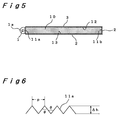
- the light source 1 is provided in close proximity to the one end surface 11a of the transparent substrate 10 formed in a concavo-convex shape, and a light reflector 1a is provided around the light source 1, as shown in Fig. 5, so that light emitted from the light source 1 is introduced into the transparent substrate 10 from the end surface 11a formed in a zigzag shape in the direction of the end side as described above.
- end surfaces 11b excluding the end surface 11a formed in a concavo-convex shape as described above and a reflecting surface 13 on the opposite side of the light emitting surface 12 for emitting the light are respectively provided with reflection sheets 2 so that the light introduced into the transparent substrate 10 is reflected by the reflection sheets 2.
- irregular reflecting portions 13a in a circular shape for irregularly reflecting the light are so formed that the farther the irregular reflecting portion 13a is apart from the light source 1, the larger the area thereof is, and a plurality of rows of irregular reflecting portions 13a are provided, as shown in Fig. 4.
- the light introduced into the transparent substrate 10 is irregularly reflected by the irregular reflecting portions 13a.
- the irregular reflecting portion 13a can be provided by applying a white paint to the reflecting surface 13, and subjecting the reflecting surface 13 to fine concavo-convex processing, for example. Further, an irregular reflecting portion 13a can be formed on the whole of the reflecting surface 13, as shown in Fig. 3.
- the light emitting surface 12 is provided with a translucent dispersion sheet 3, so that the emitted light is made uniform upon being dispersed by the dispersion sheet 3.
- the light emitted from the light source 1 provided in close proximity to the one end surface 11a of the transparent substrate 10 formed in a concavo-convex shape as described above is introduced into the transparent substrate 10 using the panel according to the present embodiment, the light is incident on the transparent substrate 10 upon being dispersed in various directions on the end surface 11a formed in a concavo-convex shape.
- the light thus incident on the transparent substrate 10 upon being dispersed in various directions is introduced into the light emitting surface 12 upon being reflected from the irregular reflecting portions 13a and portions of the reflection sheets 2, so that the light is emitted from the light emitting surface 12 through the dispersion sheet 3.
- a panel used for a surface light source device according to the embodiment in which the pitch p between the crests of the zigzag is set to 2 mm, and the difference in height ⁇ h between the crest and the trough of the zigzag is set to 1 mm, and a panel used for a surface light source device in a comparative example 1 in which the end surface 11a, to which the light source 1 is provided in close proximity, of the transparent substrate 10 is not formed in a zigzag shape but made flat, as shown in Fig. 1 and 2 are used.
- Light is emitted to the panels 3 from the light source 1 under the same conditions, and the states of the light emitted from the respective light emitting surface 12 are examined.
- each of the light emitting surfaces 12 is divided into five equal divisions in the longitudinal and transverse directions to obtain 25 portions, and the luminance in the center of each of the portions is measured.
- the average value of the luminance measured in each of the portions (average luminance) is found, and the maximum luminance and the minimum luminance are measured in the portion.
- the results are shown in the following Table 1.
- the average luminance and the uniformity ratio are improved, and no luminescent lines are produced in the vicinity of the end surface 11a of the transparent substrate 10, as compared with those in the panel in the comparative example in which the end surface 11a is made flat, whereby the entire light emitting surface 12 can be illuminated with light having uniform and sufficient brightness.
- the luminance of the light emitted from the light emitting surface 12 in the panel in the experimental example 3 in which the point angle ⁇ is set to 120° is higher than that in each of the panels in the experimental examples 1 and 2 in which the point angle ⁇ is set to 90°, whereby light having uniform and high luminance is emitted from the light emitting surface 12.
- examples of a transparent substrate 10 include one composed of a material having good light transmission properties such as acrylic resin or polycarbonate resin.
- Irregular reflecting portions 13a in a circular shape are so formed on a reflecting surface 13 of the transparent substrate 10 that the farther the irregular reflecting portion 13a is apart from a light source 1, the larger the area thereof is, and a plurality of rows of irregular reflecting portions 13a are provided, as in the above-mentioned embodiment 1.
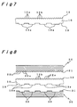
- a lot of projections 12a and recesses 12b in a fine, rounded and smooth shape are provided on a light emitting surface 12 on the opposite side of the reflecting surface 13 on which the irregular reflecting portions 13a are provided, as shown in Fig. 7.
- the reason why the projections 12a and the recesses 12b which are provided on the light emitting surface 12 are brought into a smooth shape is that if the projections 12a and the recesses 12b are not in a smooth shape, light introduced into the light emitting surface 12 is further reflected from the projections 12a and the recesses 12b, whereby only the luminance in a portion near the light source 1 is increased, and light having uniform luminance is not obtained on the whole of the light emitting surface 12.
- the light emitting surface 12 is formed by respectively setting the maximum heights Rt and Rmax of a roughness curve and a profile curve which are defined in JIS B 0601 to not less than 0.4 ⁇ m and setting the average roughness at ten points which is also defined in JIS B 0601 in the profile curve to not less than 0.3 ⁇ m in order that the light introduced into the light emitting surface 12 is emitted upon being diffused in various directions by the projections 12a and the recesses 12b.
- the light emitting surface 12 As a method of providing the light emitting surface 12 with a lot of projections 12a and recesses 12b in a fine and smooth shape, it is also possible to directly form the projections 12a and the recesses 12b on the light emitting surface 12 of the transparent substrate 10 by blasting or the like.
- the states of the projections 12a and the recesses 12b formed on each of transparent substrates 10 are not made constant, and each of the transparent substrates 10 must be subjected to blasting, whereby a lot of time and costs are required to mass-produce the panel.
- spherical beads driven into the molding surface 21 of the mold 20 include a spherical member such as garnet, glass or silica.
- the spherical beads composed of garnet, glass or silica having a particle size of #240 to #3000 and preferably, having a particle size of #500 to #1000 are uniformly blasted at atmospheric pressures of 1 to 5 from distances of 100 to 500 mm.
- a plurality of rows of recesses 32 which have the shape of a circle having a depth of approximately 10 ⁇ m and have diameters successively increased are formed by photo-etching so as to correspond to the irregular reflecting portions 13a, as shown in Fig. 8.
- the panel used for a surface light source device according to the present embodiment is fabricated by injection molding using the molds 20 and 30.
- irregular reflecting portions 13a on the reflecting surface 13 of the panel and a lot of fine and smooth projections 12a and recesses 12b on the light emitting surface 12 are formed simultaneously with the fabrication of the panel, whereby the panel can be simply fabricated.
- a method of forming the irregular reflecting portions 13a on the reflecting surface 13 of the panel is not limited to the above-mentioned method. It is also possible to provide the irregular reflecting portions 13a by shot blasting, silk screen printing or the like on the reflecting surface 13 of the panel. Further, it is also possible to provide an irregular reflecting portion 13a on the whole of the reflecting surface 12, as shown in Fig. 3.
- the light source 1 In emitting light from the light emitting surface 12 using the panel, the light source 1 is provided in close proximity to the one end surface 11a of the transparent substrate 10, and a light reflector 1a is provided around the light source 1, so that the light emitted from the light source 1 is introduced into the transparent substrate 10 from the end surface 11a, as in the conventional example shown in Fig. 1. Further, reflection sheets 2 are respectively provided on the remaining end surfaces 11b which are not in close proximity to the light source 1 and the reflecting surface 13 on which a lot of irregular reflecting portions 13a are provided, and a translucent dispersion sheet 3 is provided on the light emitting surface 12 on which the fine and smooth projections 12a and recesses 12b are found as described above.
- the light emitted from the light source 1 When the light emitted from the light source 1 is incident on the panel through the end surface 11a of the transparent substrate 10, the light is introduced into the light emitting surface 12 upon being reflected from the irregular reflecting portions 13a, the reflection sheets 2, and the like. Further, the light thus introduced into the light emitting surface 12 is emitted upon being scattered in portions of the smooth projections 12a and recesses 12 provided on the light emitting surface 12, and the light thus scattered is dispersed by the dispersion sheet 3.
- the panel used for a surface light source device in the embodiment 2 and a panel used for a surface light source device in a comparative example 2 are then compared.
- polymethyl methacrylate resin having high light transmission properties is used for a material composing the transparent substrate 10.
- the molding surfaces 21 and 31 of the molds 20 and 30 are respectively subjected to preprocessing, to bring the molding surfaces 21 and 31 into mirror surfaces.
- spherical garnet having a particle size of #800 is blasted at an atmospheric pressure of 2.5 from a distance of 200 mm at the molding surface 21 of the mold 20, to provide a lot of recesses 22a and projections 22b in a fine and smooth shape on the molding surface 21.
- a molding surface which is brought into a mirror state is used as it is.
- the recesses 32 in a circular shape which have a depth of approximately 10 ⁇ m and have diameters successively increased in the range of 0.3 to 0.85 mm are formed on the molding surface 31 by photo-etching.
- the molds 20 and 30 are used, to fabricate the panels in the embodiment 2 and the comparative example 2 each having a length of 151 mm, having a width of 212.2 mm and having a thickness of 2.5 mm by an injection machine (TD-150 manufactured by Nishin Jushi Kogyo K.K.).
- a plurality of rows of irregular reflecting portions 13a in a circular shape which has diameters successively increased in the range of 0.3 mm to 0.85 mm are formed on the reflecting surface 13, and a lot of fine and smooth projections 12a and recesses 12b are formed on the light emitting surface 12.
- a plurality of rows of irregular reflecting portions 13a similarly to those in the embodiment 2 are formed on the reflecting surface 13, while the light emitting surface 12 is flat.
- a light source 1 in a cylindrical shape is arranged in close proximity to the end surface 11a of the transparent substrate 10 on the side of the irregular reflecting portions 13a having smaller diameters, and the light reflector 1a is provided around the light source 1 in a cylindrical shape.
- Reflection sheets 2 made of polyester are respectively provided on the end surfaces 11b excluding the end surface 11a which is in close proximity to the light source 1 and the reflecting surface 13 on which the irregular reflecting portions 13a are provided.
- the light emitting surface 12 is provided with a translucent dispersion sheet 3 made of polyester for dispersing light to the light emitting surface 12.
- each of the light emitting surfaces 12 is divided into three equal divisions in the longitudinal and transverse directions to obtain nine portions, and the luminance in the center of each of the portions is measured by a luminance meter (BM-7 manufactured by Topukon K.K.).
- BM-7 manufactured by Topukon K.K.
- the average luminance and the uniformity ratio in each of the panels are found, as in the above-mentioned embodiment 1.
- the results are shown in the following Table 3. Further, rise corresponding to the pattern of the irregular reflecting portions 13a and a difference in brightness are visually evaluated. The results are also shown in the following Table 3.
- the panel in the embodiment 2 in which the projections 12a and the recesses 12b in a fine and smooth shape are formed on the light emitting surface 12 is approximately the same in the average luminance as the panel in the comparative example 2 in which the projections 12a and the recesses 12b are not formed on the light emitting surface 12. Therefore, the rise corresponding to the pattern of the irregular reflecting portions 13a and the difference in brightness are prevented from arising, whereby light having uniform and sufficient brightness is emitted from the whole of the light emitting surface 12.
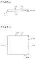
- a transparent substrate 10 is so formed that its plane is in a rectangular shape, and the thickness thereof is decreased away from an end surface 11a to which a light source 1 is provided in close proximity, as shown in Figs. 9 (A) and 9 (B), using polymethyl methacrylate resin having high light transmission properties.
- a reflecting member 14 composed of resin having light reflecting properties is integrally formed in such a manner as to be in contact with three end surfaces 11b other than the end surface 11a which is in close proximity to the light source, and a reflecting surface 13 in the above-mentioned transparent substrate 10, as shown in Figs. 10 (A) and 10 (B), and there is provided a containing section 14a containing the light source 1 upon further projecting the reflecting member 14 toward the light source 1 beyond the end surface 11a, which is in close proximity to the light source 1, of the transparent substrate 10.
- Examples of the resin having light reflecting properties used for the reflecting member 14 include one whose reflecting properties are increased by adding titanium oxide, zinc sulfide, etc. which is a white pigment to polymethyl methacrylate resin, polycarbonate resin, etc.
- the reflecting member 14 is integrally formed in such a manner as to be in contact with the transparent substrate 10 as described above, when the resin used for the reflecting member 14 and the resin used for the transparent substrate 10 differ in the coefficient of thermal expansion or the like, a load is applied to the transparent substrate 10 and the reflecting member 14 by heat or the like at the time of using the panel, whereby the transparent substrate 10 and the reflecting member 14 are deformed. Therefore, it is preferable to use as the resin used for the reflecting member 14 the same resin as the resin used for the transparent substrate 10 or resin similar thereto in properties such as the coefficient of thermal expansion.
- the light source 1 such as a cold-cathode tube is contained in the containing section 14a of the reflecting member 14, a peripheral portion of the transparent substrate 10 is pressed by a pressing member 15 in a square annular shape having reflecting properties, and the light source 1 contained in the containing section 14a is enclosed by the pressing member 15, as shown in Fig. 11.
- the light emitted in various directions from the light source 1 is reflected by the pressing member 15 and the reflecting member 14, is introduced into the end surface 11a of the transparent substrate 10 which is in close proximity to the light source 1, and is efficiently incident on the transparent substrate 10 through the end surface 11a.
- the light introduced into the transparent substrate 10 through the end surface 11a is reflected by the reflecting member 14 formed in contact with the three end surfaces 11b excluding the end surface 11a and the reflecting surface 13, and is efficiently introduced into the light emitting surface 12, whereby uniform and bright light is obtained from the entire light emitting surface 12.
- the reflecting member 14 is formed in such a manner as to be in contact with the end surfaces 11b other than the end surface 11a which is in close proximity to the light source 1, and the reflecting surface 13 in the transparent substrate 10 as described above, whereby the necessity of performing such laborious work that the reflection sheets 2 are affixed to the end surfaces 11b other than the end surface 11a and the reflecting surface 13 as in the conventional example is eliminated. Further, the possibilities that the affixed reflection sheets 2 are stripped by themselves, and the light introduced into the transparent substrate 10 is not reflected from portions where the reflection sheets 2 are stripped, whereby a dark portion partially occurs as in the conventional example are eliminated. Therefore, uniform light is stably emitted from the whole of the light emitting surface 12 of the transparent substrate 10.
- a plurality of rows of irregular reflecting portions 13a for irregularly reflecting light so provided that the farther the irregular reflecting portion 13a is apart from the light source 1, the larger the area thereof is, as shown in Fig. 2, an irregular reflecting portion 13a is formed on the whole of the reflecting surface 13, as shown in Fig. 3, a translucent dispersion sheet 4 is arranged on the light emitting surface 12 so that emitted light is made uniform upon being dispersed by the dispersion sheet 4, as in the conventional example.
- the light emitting surface 12 is further provided with a lens sheet so that emitted light can be gathered in a direction perpendicular to the light emitting surface 12.
- the irregular reflecting portions 13 for irregularly reflecting light are provided on the reflecting surface 13 of the transparent substrate 10 in order to prevent the irregular reflecting portions 13 from being seen as if the pattern thereof was raised and prevent a difference in brightness from partially arising, a lot of projections 12a and recesses 12b in a fine and smooth shape are provided on the light emitting surface 12 of the transparent substrate 10, as shown in Fig. 12. Further, in order to prevent luminescent lines from being produced along the end surface 11a to which the light source 1 is provided in close proximity in the vicinity of the end surface 11a, the end surface 11a can be also formed in a concavo-convex shape in the direction of its end side, as shown in Fig. 13.
Landscapes
- Physics & Mathematics (AREA)
- General Physics & Mathematics (AREA)
- Optics & Photonics (AREA)
- Nonlinear Science (AREA)
- Mathematical Physics (AREA)
- Chemical & Material Sciences (AREA)
- Crystallography & Structural Chemistry (AREA)
- Planar Illumination Modules (AREA)
- Liquid Crystal (AREA)
Applications Claiming Priority (6)
| Application Number | Priority Date | Filing Date | Title |
|---|---|---|---|
| JP317205/95 | 1995-11-10 | ||
| JP7317205A JPH09138310A (ja) | 1995-11-10 | 1995-11-10 | 面光源用パネル及びその製造方法 |
| JP7326561A JPH09145936A (ja) | 1995-11-20 | 1995-11-20 | 面光源用パネル |
| JP326561/95 | 1995-11-20 | ||
| JP21811/96 | 1996-01-12 | ||
| JP8021811A JPH09197403A (ja) | 1996-01-12 | 1996-01-12 | 面光源用パネル |
Publications (2)
| Publication Number | Publication Date |
|---|---|
| EP0773402A2 true EP0773402A2 (de) | 1997-05-14 |
| EP0773402A3 EP0773402A3 (de) | 1997-10-29 |
Family
ID=27283573
Family Applications (1)
| Application Number | Title | Priority Date | Filing Date |
|---|---|---|---|
| EP96117854A Withdrawn EP0773402A3 (de) | 1995-11-10 | 1996-11-07 | Platte für Oberflächenlichtquellen-Vorrichtung |
Country Status (4)
| Country | Link |
|---|---|
| US (1) | US5926033A (de) |
| EP (1) | EP0773402A3 (de) |
| KR (1) | KR970028720A (de) |
| TW (1) | TW404532U (de) |
Cited By (4)
| Publication number | Priority date | Publication date | Assignee | Title |
|---|---|---|---|---|
| WO1998027382A1 (de) * | 1996-12-16 | 1998-06-25 | Robert Bosch Gmbh | Beleuchtungseinheit |
| EP1194741A4 (de) * | 1999-07-08 | 2002-09-04 | Physical Optics Corp | VORRICHTUNG ZUR RüCKSEITIGEN BELEUCHTUNG MIT LICHTLEITEROPTIK MIT INTEGRIERTER OBERFLäCHENSTREUEINHEIT |
| WO2003048821A1 (en) * | 2001-11-30 | 2003-06-12 | Equity Industries Corp. | Clocks with diffusion reflector lighting |
| EP2889658A4 (de) * | 2012-08-21 | 2016-07-20 | Dahai Zhang | Oberflächenstruktur für eine lichtleiterplatte sowie anwendung davon und herstellungsverfahren dafür |
Families Citing this family (27)
| Publication number | Priority date | Publication date | Assignee | Title |
|---|---|---|---|---|
| JPH10144122A (ja) * | 1996-11-06 | 1998-05-29 | Enplas Corp | サイドライト型面光源装置 |
| JP3615355B2 (ja) * | 1997-06-04 | 2005-02-02 | 株式会社エンプラス | サイドライト型面光源装置及び導光板 |
| JP3422917B2 (ja) * | 1997-11-05 | 2003-07-07 | 株式会社エンプラス | サイドライト型面光源装置及び液晶表示装置 |
| GB9807204D0 (en) * | 1998-04-04 | 1998-06-03 | Ici Plc | An edge-lit illumination system |
| JP3379043B2 (ja) * | 1998-06-29 | 2003-02-17 | ミネベア株式会社 | 面状照明装置 |
| TW487170U (en) * | 1998-07-17 | 2002-05-11 | Enplas Corp | Guide plate, surface light source device of side light type and liquid crystal display |
| US6183099B1 (en) * | 1999-06-09 | 2001-02-06 | Timex Corporation | Light guide for illuminating a dial |
| CN1174182C (zh) * | 1999-07-21 | 2004-11-03 | 日本板硝子株式会社 | 平面显示灯及光散射体图形的形成方法 |
| JP4001736B2 (ja) * | 2001-10-23 | 2007-10-31 | アルプス電気株式会社 | 面発光装置及び液晶表示装置 |
| TWI247142B (en) * | 2002-11-20 | 2006-01-11 | Hon Hai Prec Ind Co Ltd | Light guide plate used for backlight module |
| TWI273292B (en) * | 2002-12-31 | 2007-02-11 | Hon Hai Prec Ind Co Ltd | Light guide plate and backlight system using the same |
| TW566564U (en) * | 2003-01-29 | 2003-12-11 | Hon Hai Prec Ind Co Ltd | Back light module and liquid crystal display using the same |
| TW587800U (en) * | 2003-03-07 | 2004-05-11 | Behavior Tech Computer Corp | Keyboard with a backlight module |
| JP4247035B2 (ja) * | 2003-04-21 | 2009-04-02 | シチズン電子株式会社 | 面状光源 |
| US6879182B1 (en) * | 2003-05-01 | 2005-04-12 | Lattice Semiconductor Corporation | CPLD with multi-function blocks and distributed memory |
| US7281834B2 (en) * | 2004-01-28 | 2007-10-16 | Photoglow, Inc. | Method and apparatus for image illumination using self-contained luminaire |
| TWI271583B (en) * | 2004-03-09 | 2007-01-21 | Au Optronics Corp | Light guide of backlight unit |
| CN100437268C (zh) * | 2004-07-09 | 2008-11-26 | 鸿富锦精密工业(深圳)有限公司 | 导光板模具及其制备方法 |
| DE102004046386A1 (de) * | 2004-09-24 | 2006-04-06 | Schefenacker Vision Systems Germany Gmbh & Co. Kg | Lichtleiter für Leuchten, insbesondere für Leuchten von Kraftfahrzeugen |
| CN100370329C (zh) * | 2004-11-12 | 2008-02-20 | 清华大学 | 导光板和背光模组 |
| CN100445827C (zh) * | 2004-11-18 | 2008-12-24 | 清华大学 | 导光板和背光模组 |
| TWI263098B (en) * | 2005-02-16 | 2006-10-01 | Au Optronics Corp | Backlight module |
| JP5168813B2 (ja) * | 2006-04-14 | 2013-03-27 | ソニー株式会社 | 光学シート、バックライト装置および液晶表示装置 |
| US8870434B2 (en) * | 2011-09-12 | 2014-10-28 | Skc Haas Display Films Co., Ltd. | Asymmetric serrated edge light guide film having circular base segments |
| US8858058B2 (en) * | 2011-09-12 | 2014-10-14 | Skc Haas Display Films Co., Ltd. | Asymmetric serrated edge light guide film having circular base segments |
| GB2522400B (en) * | 2013-10-29 | 2020-06-10 | Calsonic Kansei Uk Ltd | A light conduit for an illumination apparatus |
| KR102421752B1 (ko) * | 2019-12-18 | 2022-07-15 | 주식회사 케이티앤지 | 카트리지 및 에어로졸 생성 장치 |
Family Cites Families (6)
| Publication number | Priority date | Publication date | Assignee | Title |
|---|---|---|---|---|
| JP3204999B2 (ja) * | 1990-06-26 | 2001-09-04 | 株式会社スタンレー滋賀製作所 | エッジライトパネル |
| JP2692025B2 (ja) * | 1992-01-24 | 1997-12-17 | スタンレー電気株式会社 | 面状発光体装置 |
| US5303322A (en) * | 1992-03-23 | 1994-04-12 | Nioptics Corporation | Tapered multilayer luminaire devices |
| TW334523B (en) * | 1994-03-02 | 1998-06-21 | Toso Kk | Back light |
| US5575549A (en) * | 1994-08-12 | 1996-11-19 | Enplas Corporation | Surface light source device |
| JP3213496B2 (ja) * | 1994-11-30 | 2001-10-02 | シャープ株式会社 | 照明装置 |
-
1996
- 1996-11-04 TW TW088213712U patent/TW404532U/zh not_active IP Right Cessation
- 1996-11-06 US US08/744,667 patent/US5926033A/en not_active Expired - Fee Related
- 1996-11-07 EP EP96117854A patent/EP0773402A3/de not_active Withdrawn
- 1996-11-09 KR KR1019960053023A patent/KR970028720A/ko not_active Ceased
Non-Patent Citations (1)
| Title |
|---|
| None |
Cited By (5)
| Publication number | Priority date | Publication date | Assignee | Title |
|---|---|---|---|---|
| WO1998027382A1 (de) * | 1996-12-16 | 1998-06-25 | Robert Bosch Gmbh | Beleuchtungseinheit |
| US6330386B1 (en) | 1996-12-16 | 2001-12-11 | Robert Bosch Gmbh | Lightening unit |
| EP1194741A4 (de) * | 1999-07-08 | 2002-09-04 | Physical Optics Corp | VORRICHTUNG ZUR RüCKSEITIGEN BELEUCHTUNG MIT LICHTLEITEROPTIK MIT INTEGRIERTER OBERFLäCHENSTREUEINHEIT |
| WO2003048821A1 (en) * | 2001-11-30 | 2003-06-12 | Equity Industries Corp. | Clocks with diffusion reflector lighting |
| EP2889658A4 (de) * | 2012-08-21 | 2016-07-20 | Dahai Zhang | Oberflächenstruktur für eine lichtleiterplatte sowie anwendung davon und herstellungsverfahren dafür |
Also Published As
| Publication number | Publication date |
|---|---|
| US5926033A (en) | 1999-07-20 |
| EP0773402A3 (de) | 1997-10-29 |
| TW404532U (en) | 2000-09-01 |
| KR970028720A (ko) | 1997-06-24 |
Similar Documents
| Publication | Publication Date | Title |
|---|---|---|
| US5926033A (en) | Surface light source panel for uniform luminance | |
| US5130898A (en) | Background lighting apparatus for liquid crystal display | |
| US5709447A (en) | Lighting device | |
| US6275338B1 (en) | Light regulation device | |
| US5775791A (en) | Surface emission apparatus | |
| US6981792B2 (en) | Backlight device and liquid crystal display device | |
| KR100484365B1 (ko) | 사이드라이트형면광원장치,액정디스플레이및도광판 | |
| EP0592241A1 (de) | Flächige Beleuchtungseinrichtung | |
| US20040109105A1 (en) | Backlight unit and liquid crystal display device | |
| KR19990083108A (ko) | 렌즈 필름 및 면광원 장치 | |
| JP2002048921A (ja) | 導光板、面光源装置及び表示装置 | |
| JPH07159607A (ja) | 光制御シート及びこれを備えた面状発光装置 | |
| JP3067149B2 (ja) | 照明装置及びそれを用いた液晶表示器 | |
| KR100821995B1 (ko) | 도광판유닛 및 백라이트 | |
| KR102176263B1 (ko) | 음각 패턴과 양각 패턴을 구비한 도광판 및 이를 이용한 백라이트 유닛, 이를 포함하는 디스 플레이 장치 | |
| KR20030080764A (ko) | 직하형 백라이트 장치 | |
| KR20190134439A (ko) | 음각 패턴을 구비한 도광판 및 이를 이용한 백라이트 유닛 | |
| US6211929B1 (en) | Surface light source device of side light type and liquid crystal display | |
| JP3283923B2 (ja) | エッジライト用導光体の製造方法 | |
| JPH08146225A (ja) | バックライト | |
| JPH06289393A (ja) | 照明装置 | |
| KR100344474B1 (ko) | 도광판및그것을이용한평면조광장치 | |
| JP3394623B2 (ja) | 導光板及びそれを用いた平面照光装置 | |
| KR100583476B1 (ko) | 미세 크기의 다각형 프리즘 집합체로 구성된 빛확산판 | |
| KR100373442B1 (ko) | 광반사 구조체를 갖는 도광판 |
Legal Events
| Date | Code | Title | Description |
|---|---|---|---|
| PUAI | Public reference made under article 153(3) epc to a published international application that has entered the european phase |
Free format text: ORIGINAL CODE: 0009012 |
|
| AK | Designated contracting states |
Kind code of ref document: A2 Designated state(s): DE FR GB |
|
| PUAL | Search report despatched |
Free format text: ORIGINAL CODE: 0009013 |
|
| AK | Designated contracting states |
Kind code of ref document: A3 Designated state(s): DE FR GB |
|
| 17P | Request for examination filed |
Effective date: 19980126 |
|
| 17Q | First examination report despatched |
Effective date: 20020308 |
|
| STAA | Information on the status of an ep patent application or granted ep patent |
Free format text: STATUS: THE APPLICATION HAS BEEN WITHDRAWN |
|
| 18W | Application withdrawn |
Effective date: 20030708 |